Table of Contents
Advertisement
Quick Links
Service
Service
Service
Service
Service
Service Manual
Copyright 2005 Philips Consumer Electronics B.V. Eindhoven, The Netherlands
©
All rights reserved. No part of this publication may be reproduced, stored in a retrieval system or
transmitted, in any form or by any means, electronic, mechanical, photocopying, or otherwise
without the prior permission of Philips.
Published by KC-ET0430 Service Audio Printed in The Netherlands Subject to modification
VERSION 1.0
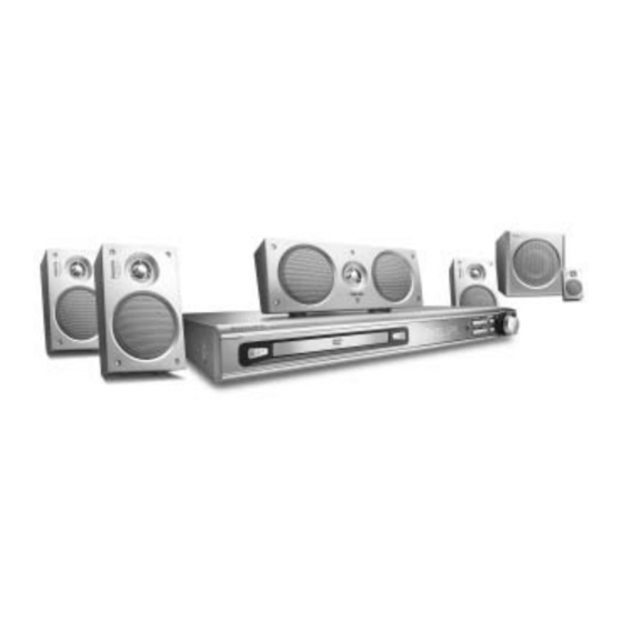
MX2600/77/78
CLASS 1
LASER PRODUCT
GB
3139 785 31910
Advertisement
Table of Contents

Summary of Contents for Philips MX2600/77/78
- Page 1 Service Manual CLASS 1 LASER PRODUCT Copyright 2005 Philips Consumer Electronics B.V. Eindhoven, The Netherlands © All rights reserved. No part of this publication may be reproduced, stored in a retrieval system or transmitted, in any form or by any means, electronic, mechanical, photocopying, or otherwise without the prior permission of Philips.
- Page 2 LOCATION OF PC BOARDS MAIN PCB POWER PCB PH PCB VERSION VARIATION: Type /Versions MX2600 Features & Board in used: /77/78 Rotary Encoder (volume control) Aux Input Digital Output Line Output Progressive scan Power supply (110 / 220 V~)
-
Page 3: Specifications
Audio DAC ..........24 Bits / 96 kHz Frequency Response ....4 Hz – 20 kHz (44.1 kHz) ............4 Hz – 22 kHz (48 kHz) Digital Output ........SPDIF (Sony Philips ............. digital interface) Coaxial - Dolby Digital ......... IEC 60958, IEC 61937... -
Page 4: Measurement Setup
MEASUREMENT SETUP Tuner FM Bandpass LF Voltmeter 250Hz-15kHz e.g. PM2534 e.g. 7122 707 48001 RF Generator e.g. PM5326 S/N and distortion meter e.g. Sound Technology ST1700B Use a bandpass filter to eliminate hum (50Hz, 100Hz) and disturbance from the pilottone (19kHz, 38kHz). Tuner AM (MW,LW) Bandpass LF Voltmeter... -
Page 5: Service Aids
SERVICE AIDS Service Tools: Universal Torx driver holder .........4822 395 91019 Torx bit T10 150mm ...........4822 395 50456 Torx driver set T6-T20 .........4822 395 50145 Torx driver T10 extended ........4822 395 50423 Compact Disc: SBC426/426A Test disc 5 + 5A ......4822 397 30096 SBC442 Audio Burn-in test disc 1kHz ....4822 397 30155 SBC429 Audio Signals disc .........4822 397 30184 Dolby Pro-logic Test Disc ........4822 395 10216... -
Page 6: Class 1 Laser Product
WAARSCHUWING WARNING Alle IC’s en vele andere halfgeleiders zijn All ICs and many other semi-conductors are gevoelig voor electrostatische ontladingen susceptible to electrostatic discharges (ESD). (ESD). Careless handling during repair can reduce life Onzorgvuldig behandelen tijdens reparatie kan drastically. de levensduur drastisch doen verminderen. When repairing, make sure that you are Zorg ervoor dat u tijdens reparatie via een connected with the same potential as the mass... - Page 7 You will find this and more technical information • Use only lead-free solder alloy Philips SAC305 with within the “magazine”, chapter “workshop news”. order code 0622 149 00106. If lead-free solder-paste is required, please contact the manufacturer of your For additional questions please contact your local solder-equipment.
- Page 8 REPAIR INSTRUCTIONS (1 of 2)
- Page 9 REPAIR INSTRUCTIONS (2 of 2)
- Page 10 DISASSEMBLY INSTRUCTIONS Dismantling of the DVD Module 1) Loosen 4 screws "A" to remove the DVD Module as shown in figure 4. Dismantling of the Front Panel Assembly 1) Open the DVD Tray by using the Open/Close Button 2) Return the set to its upright position and remove the Tray while the Set is ON and disconnect the mains supply after Cover as shown in Figure 3 and close the tray manually removing the Tray Cover.
-
Page 11: Service Positions
SERVICE POSITIONS Dismantling of the Main & Tuner PCB 1) Loosen 10 screw " D " at the back panel as shown in figure Service position A 2) Loosen 4 screw " E " on the top of main board and loosen 2 screw on the bottom panel as shown in figure 7 Figure 6 Note: In some service positions the components or copper patterns of one board may risk touching its neighbouring pc... -
Page 12: Block Diagram
BLOCK DIAGRAM... -
Page 13: Wiring Diagram
WIRING DIAGRAM... -
Page 14: Ftd Display Pin Assignment
FTD DISPLAY PIN ASSIGNMENT KEY (CONTROL / STANDBY / VOL) BOARD (2G - 10G) PIN CONNECTION PIN NO. 31~23 CONNECTION P13 P12 ## Note ## 1. Fn: Filament pin 2. NP : No Pin 3. NX : No Extended Pin 4. - Page 15 CIRCUIT DIAGRAM - KEY BOARD C2201 R2251 C2202 R2252 C2204 R2253 C2206 R2254 C2207 R2255 C2208 RB201 C2209 RB202 C2212 RB202A C2213 RB202B C2214 RB203A C2215 RB203B C2216 SN2201 C2217 TA2201 C2218 TA2202 C2219 TA2203 C2220 TA2204 C2221 TA2205 C2222 TA2206 C2223 TA2207...
- Page 16 PCB LAYOUT - KEY BOARD (TOP) C2204 D2201 RB202 TA2201 TA2207 C2207 D2202 RB202A TA2202 TA2208 C2208 DP2201 RB202B TA2203 VR2201 C2213 LD2201 RB203A TA2204 XL2201 C2217 R2228 RB203B TA2205 ZD2201 C2223 RB201 SN2201 TA2206 PCB LAYOUT - KEY BOARD (BOTTOM) C2201 C2219 R2227...
- Page 17 IC2201 (HT480051) VOLTAGE 4.9 4.9 IC2202 (TP6311) VOLTAGE 19.7 -22.2 -11.2 -19.9 -17.8 -21 -15.6 -13.4 -20 -13.4 -20 -22.4 -18 -20.3 -13.6 -15.8 -11.4 -4.6 -22.6 -20.4 -20.4 -20.4 -20.4 -20.4 -20.4 VOLTAGE VOLTAGE -20.4 -20.4 -20.5 -20.4 Q2201 (2SA733) Q2202 (2SA733) Q2203 (2SA733) VOLTAGE...
-
Page 18: Tuner Adjustment Table
TUNER ADJUSTMENT TABLE Waverange Input frequency Input Tuned to Adjust Output Scope/Voltmeter VARICAP ALIGNMENT 108MHz 6.5V ±1.2V check 87.5 - 108MHz (50kHz grid) 87.5MHz check 1.0V ±0.5V 1602KHz check 7.8V ± 0.2V 1.1V ± 0.5V 531KHz T005 530-1710kHz (10kHz grid) TUNER BOARD ( 21L / 21L / 37S ) check... - Page 19 CIRCUIT DIAGRAM - TUNER BOARD ANT001 A1 R004 C002 R005 C005 R006 C007 R010 C006 R011 C008 R015 C009 R016 R017 R018 R019 C010 R020 C011 R021 C012 R023 C013 R024 C014 R025 C015 R026 C016 R027 C019 R028 C020 R029 C021 R030...
- Page 20 PCB LAYOUT - TUNER BOARD (TOP) ANT001 C025 D002 IF003 JWP8 T001 VD001 C005 C030 D003 JWP2 JWP9 T002 VD002 C006 C035 D004 JWP3 T003 VD003 C007 C047 D005 JWP4 L001 T005 VD004 C009 CN001 IC001 JWP5 Q001 T006 VR001 C019 CN002 IF001...
- Page 21 PCB LAYOUT - TUNER BOARD (BOTTOM) C013 C023 C037 C048 R005 R019 R028 C014 C026 C038 C050 R006 R020 R029 C001 C015 C029 C039 C052 R007 R021 R030 C002 C016 C031 C040 IC001 R010 R023 R031 C008 C020 C032 C041 Q003 R011 R024...
- Page 22 VOLTAGES IC001 (TEA5757H) VOLTAGE(FM) 2.1 0.01 0.01 0.01 0.01 0.01 7.21 4.49 0.7 1.24 0.83 0.77 0.63 0.64 1.01 0.01 1.15 1.15 VOLTAGE(AM) 2.1 0.01 0.01 0.01 0.01 0.01 7.45 1.12 1.36 0.58 1.24 0.18 0.77 0.63 0.64 1.01 0.01 1.15 1.15 VOLTAGE(FM) 1.94 10.9 9.13 1.26 1.92 0.01 0.19 0.52 0.2 0.01 0.01 1.43 0.75 1.43 0.7 1.43 0.62 1.35 1.02 1.34...
- Page 23 DVD LOADER It is not recommended for component repair on this Module but to replace the major assembly when it becomes defective. Therefore limited service parts list are published in this chapter. TABLE OF CONTENTS Explorer View (DVD Loader) ........... 7-2...
- Page 24 Explorer view...
-
Page 25: Main Board
ES6628F INTERNAL IC DIAGRAM MAIN BOARD AM5868S INTERNAL IC DIAGRAM OP1N+ OP1N- VINLD VCTL OP1OUT VCC2 VOLD- VOLD+ VOTK- MUTE BIAS VINTK VOTK+ Vcc2 MUTE Spindle Actiator Driver(4X) Driver(6X) Thermal Shut down Vcc2 Vcc2 Vcc1 Sled Actiator Driver(6X) Driver(4X) Pre-DRV DRIVER PGND Vcc1... - Page 26 VOLTAGES IC201 (ES6629) IC401 (RC4558) IC903 (BA50BC0T) Q301 (2SC1623) Pin No. Pin No. PIN NO 1 PIN NO 1 Voltage 8.6 Voltage 0.8 Voltage 3.3 1.77 1.77 1.77 Voltage PIN NO 21 IC402 (RC4558) Q401 (KTC3875) Q402 (KTC3875) Voltage 3.3 2.8 3.1 0.2 3.3 1.3 1.3 3.3 1.4 1.3 1.3 1.2 1.3...
- Page 27 CIRCUIT DIAGRAM (1)- MAIN BOARD C301A1 C483C2 C3306B1 D401B2 Q951D1 R483B3 R3204B1 C302A1 C484C2 C3307B1 D501D3 Q952D1 R484B3 R3205A1 C303A1 C485C2 C3308B1 D502C4 Q954D1 R485B3 R3206B1 C304A1 C486C2 C4007C2 D503D4 Q955D1 R486B3 R3207A1 C311A2 C487C2 C4008C2 D504D4 Q957D1 R487B2 R3208B1 C312A2 C488C2 C4009C2...
- Page 28 CIRCUIT DIAGRAM (2)- MAIN BOARD C201 C354 C2026 D3 R208 R853 C202 C355 C2027 D3 R210 R854 C203 C356 C2028 D3 R211 R855 C204 C357 C2029 D3 R212 R865 C205 C358 C2030 D4 R213 R866 C206 C359 C2031 D4 R214 R868 C207 C360...
- Page 29 PCB LAYOUT - MAIN BOARD (TOP) C201 B6 C235 A5 C274 B4 C313 C4 C367 C6 C417 B4 C434 B3 C454 B3 C473 B3 C527 C1 C808 A6 C832 A6 C905 A1 C982 C3 C4203 B1 C5089 D301 D508 IC207 IC503 JMP5 L957...
- Page 30 PCB LAYOUT - MAIN BOARD (BOTTOM) C214 C244 C279 C531 C902 C976 C2026 C6 C2308 A4 C3308 A5 C5099 C4 C5206 A4 IC3201 C4 L814 R216 R543 R922 R4006 B2 C215 C245 C282 C532 C904 C980 C2027 A5 C2356 C4 C4007 B2 C5103 D4 C5207 C5...
- Page 31 POWER+PH1+PH2 BOARD...
- Page 32 CIRCUIT DIAGRAM - POWER BOARD C904 C905 C906 C908 C909 C910 C911 C912 C913 C914 C922 C923 C924 C925 C927 C928 C929 C930 C931 C932 C933 C934 C935 CN901 CN901 CN905 CN905 CN905 CN909 CN909 CN911 CN911 CN912 CN912 D901 D902 D903 D904...
- Page 33 PCB LAYOUT - POWER BOARD C5013 C5014 C904 C905 C906 C907 C908 C909 C910 C911 C912 C913 C914 C922 C923 C924 C925 C927 C928 C929 C930 C931 C932 C933 C934 C935 C938 CN901 CN905 CN909 CN911 CN912 D901 D902 D903 D904 D906 D907...
-
Page 34: Mechanical Exploded View
10-1 10-1 MECHANICAL EXPLODED VIEW... - Page 35 MECHANICAL & ACCESSORIES PART LIST ELECTRICAL PARTS LIST-MAIN WASHER PCB ASS’Y MISCELLANEOUS JK401 9965 000 24074 RCA JACK 6P WHTX3/REDX3 AXIAL MISCELLANEOUS JK501 9965 000 27077 SPK JACK 6P RD-WT-GN 9965 000 32737 DVD LOADER ME M04S-1 JK502 9965 000 27078 SPK JACK 6P GY-BU-PURPLE 9965 000 32738 MAIN WASHER PCB ASS’Y...
- Page 36 ZD401 9965 000 26930 CHIP ZENER 5.6V 0.05 0.5W (E2) S IC902 9965 000 26945 IC 3PIN BA50BC0T TO220FP ROHM PB ZD402 9965 000 26930 CHIP ZENER 5.6V 0.05 0.5W (E2) S IC903 9965 000 26945 IC 3PIN BA50BC0T TO220FP ROHM PB ZD501 9965 000 27086 CHIP ZENER 9.1V 5% 0.5W (F4) S ZD801 9965 000 26931...
- Page 37 Q003 9965 000 27004 XISTR PNP BF550 SOT23 PHILIPS Q003 9940 000 00921 XISTR PNP 2SA812 HFE:200-400 IC001 9965 000 27003 IC 44 PIN TEA5757H QFP44 PHILIPS Note: Only the parts mentioned in this list are normal service spare parts.