Table of Contents
Advertisement
Quick Links
Advertisement
Table of Contents

Related Manuals for Zenith LX-140

Summary of Contents for Zenith LX-140
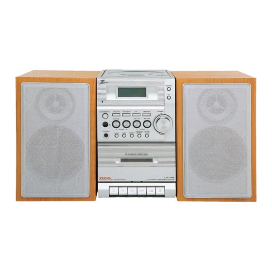
- Page 1 MICRO COMPONENT...
- Page 2 [CONTENTS] ❍ SECTION 1. GENERAL • SERVICING PRECAUTIONS ..........1-2 •...
-
Page 3: Section 1. General
SECTION 1. GENERAL ❏ SERVICING PRECAUTIONS NOTES REGARDING HANDLING OF THE PICK-UP 1. Notes for transport and storage 1) The pick-up should always be left in its conductive bag until immediately prior to use. 2) The pick-up should never be subjected to external pressure or impact. Storage in conductive bag Drop impact 2. -
Page 4: Notes Regarding Compact Disc Player Repairs
NOTES REGARDING COMPACT DISC PLAYER REPAIRS 1. Preparations 1) Compact disc players incorporate a great many ICs as well as the pick-up (laser diode). These components are sensitive to, and easily affected by, static electricity. If such static electricity is high voltage, components can be damaged, and for that reason components should be handled with care. -
Page 5: Esd Precautions
❏ ESD PRECAUTIONS Electrostatically Sensitive Devices (ESD) Some semiconductor (solid state) devices can be damaged easily by static electricity. Such components commonly are called Electrostatically Sensitive Devices (ESD). Examples of typical ESD devices are integrated circuits and some field-effect transistors and semiconductor chip components. The following techniques should be used to help reduce the incidence of component damage caused by static electricity. -
Page 6: Specifications
❏ SPECIFICATIONS - 1-5 -... - Page 7 MEMO - 1-6 -...
-
Page 8: Section 2. Electrical
SECTION 2. ELECTRICAL ❏ ADJUSTMENTS This set has been aligned at the factory and normally will not require further adjustment. As a result, it is not recommended that any attempt is made to modificate any circuit. If any parts are replaced or if any- one tampers with the adjustment, realignment may be necessary. -
Page 9: Troubleshooting
❏ TROUBLESHOOTING • CD PART - 2-2 -... - Page 10 • OPEN CLOSE NG - 2-3 -...
- Page 11 • “ READING ” DISPLAY CHECK (= ONLY “CD “DISPLAY) - 2-4 -...
- Page 12 • READING OK CHECK (= “NO DISC” DISPLAY) - 2-5 -...
- Page 13 • READING OK CHECK #A (= “NO DISC” DISPLAY) - 2-6 -...
- Page 14 • READING OK CHECK #B (= “NO DISC” DISPLAY) - 2-7 -...
- Page 15 • READING OK CHECK #C (= “NO DISC” DISPLAY) - 2-8 -...
- Page 16 • READING OK CHECK #D (= “NO DISC” DISPLAY) - 2-9 -...
- Page 17 • READING OK CHECK # E (= “NO DISC” DISPLAY) - 2-10 -...
- Page 18 ❏ WAVEFORMS OF MAKOR CHECK POINT - 2-11 -...
- Page 19 #4. SPINDLE DRIVE AND MOTOR WAVEFORM #5. TRACK DRIVE AND MOTOR WAVEFORM (IC503 pin6, 1 2) when TOC reading (TP560, IC503 pin23) during normal play #6. RF, TRACKING AND FOCUS ERROR WAVEFORM (IC502 pin8, 2 1 , 23) during normal play - 2-12 -...
-
Page 20: Audio Part
❏ AUDIO PART - 2-13 -... - Page 21 - 2-14 -...
- Page 22 - 2-15 -...
- Page 23 - 2-16 -...
- Page 24 FM(TU101) Troubleshooting Check the 12V input of TU101 pin6 Check the 12V of Q102 “E” Check the Power circuit Check the “LOW” of IC103 pin7 Refer to “IC103 Check the “High” of TU101 Pin5 Troubleshooting” Replace the Q102 Check the OSC waveform of TU101 pin8 Replace the TU101 Refer to “IC102 Troubleshooting”...
- Page 25 IC103 Troubleshooting Check the Power input of IC103 pin17 Refer to “Power Troubleshooting” X104 oscillation Repleace the X104 Check the Clock of CE, DI, DO, CLK Refer to “IC103 Troubleshooting” CE: Chip Enable DI: Data Input (from u-com) DO: Data Output (to u-com) CLK: Tuner mode clock Check the operation Repleace the IC103...
- Page 26 PLAY Check the B+ Power to LEAF Switch Check the signal to IC202 pin4, 11 Check the output to speaker Check the SW201 and HEAD connector Check the CN202 Checks the B+ power to Q201 “E” Check the CN201 Check the CN901 pin8, 9 and IC903 output Check the signal input of IC201 pin4, 11 Check the oscillation of L201 Check the B+ of LEAF...
- Page 27 MEMO - 2-20 -...
- Page 28 ❏ BLOCK DIAGRAM 2-21 2-22...
-
Page 29: Schematic Diagrams
❏ SCHEMATIC DIAGRAMS • FRONT/POWER SCHEMATIC DIAGRAM 2-23 2-24... - Page 30 • MAIN/DECK SCHEMATIC DIAGRAM 2-25 2-26...
- Page 31 • TUNER SCHEMATIC DIAGRAM 2-27 2-28...
- Page 32 • CDP SCHEMATIC DIAGRAM 2-29 2-30...
-
Page 33: Wiring Diagram
❏ WIRING DIAGRAM 2-31 2-32... -
Page 34: Printed Circuit Diagrams
❏ PRINTED CIRCUIT DIAGRAMS • FRONT P.C. BOARD 2-33 2-34... - Page 35 • MAIN P.C. BOARD 2-35 2-36...
- Page 36 • CDP P.C. BOARD 2-37 2-38...
-
Page 37: Internal Block Diagram Of Ics
❏ INTERNAL BLOCK DIAGRAM OF ICs I IC300 LC87F73C8A 1) Pin Assignment - 2-39 -... -
Page 38: Block Diagram
I IC601 TDA7468D 1) BLOCK DIAGRAM - 2-40 -... -
Page 39: Pin Connection
2) PIN CONNECTION - 2-41 -... - Page 40 I IC301 BU1923 1) BLOCK DIAGRAM - 2-42 -...
- Page 41 I IC102LA1837 1) BLOCK DIAGRAM I IC102LA1837 2) Test Circuit Diagram - 2-43 -...
- Page 42 I IC103 LC72131D 1) Pin Assignments - 2-44 -...
- Page 43 I IC201 AN7312 1) BLOCK DIAGRAM I IC701 LA4631 1) BLOCK DIAGRAM - 2-45 -...
-
Page 44: Input Function
I IC504 M12L16161A Synchronous DRAM • PIN Definitions NAME INPUT FUNCTION System Clock Active on the positive going edge to sample all inputs. Chip Select Disables or enables device operation by masking or enabling all inputs except CLK, CKE and L(U)DQM. Clock Enable Masks system clock to freeze operation from the next clock cycle. -
Page 45: Section 3. Exploded Views
SECTION 3. EXPLODED VIEWS • CABINET AND MAIN FRAME SECTION NOTE) Refer to “SECTION 5 REPLACEMENT PARTS LIST” in order to look for the part number of each part. Caution point A43: Front + Power Array Assembly. A46: Main + TP Deck + Tuner Array Assembly. -
Page 46: Section 4. Speaker Section
SECTION 4. SPEAKER SECTION ❏ MODEL: LXS-M140 - 4-1 -... - Page 47 MEMO - 4-2 -...