Table of Contents
Advertisement
Quick Links
Advertisement
Table of Contents

Related Manuals for Asus AAEON FWS-7830


Summary of Contents for Asus AAEON FWS-7830
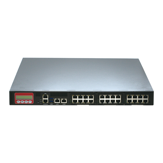
- Page 1 FWS-7830 Network Appliance User’s Manual 2 Last Updated: July 2, 2019...
- Page 2 Copyright Notice This document is copyrighted, 2019. All rights are reserved. The original manufacturer reserves the right to make improvements to the products described in this manual at any time without notice. No part of this manual may be reproduced, copied, translated, or transmitted in any form or by any means without the prior written permission of the original manufacturer.
- Page 3 Acknowledgement All other products’ name or trademarks are properties of their respective owners. Microsoft Windows is a registered trademark of Microsoft Corp. Intel, Pentium, Celeron, and Xeon are registered trademarks of Intel Corporation Core, Atom are trademarks of Intel Corporation ...
- Page 4 Packing List Before setting up your product, please make sure the following items have been shipped: Item Quantity FWS-7830 If any of these items are missing or damaged, please contact your distributor or sales representative immediately. Preface...
- Page 5 About this Document This User’s Manual contains all the essential information, such as detailed descriptions and explanations on the product’s hardware and software features (if any), its specifications, dimensions, jumper/connector settings/definitions, and driver installation instructions (if any), to facilitate users in setting up their product. Users may refer to the product page on AAEON.com for the latest version of this document.
- Page 6 Safety Precautions Please read the following safety instructions carefully. It is advised that you keep this manual for future references All cautions and warnings on the device should be noted. All cables and adapters supplied by AAEON are certified and in accordance with the material safety laws and regulations of the country of sale.
- Page 7 As most electronic components are sensitive to static electrical charge, be sure to ground yourself to prevent static charge when installing the internal components. Use a grounding wrist strap and contain all electronic components in any static-shielded containers. If any of the following situations arises, please the contact our service personnel: Damaged power cord or plug Liquid intrusion to the device iii.
- Page 8 FCC Statement This device complies with Part 15 FCC Rules. Operation is subject to the following two conditions: (1) this device may not cause harmful interference, and (2) this device must accept any interference received including interference that may cause undesired operation.
- Page 9 China RoHS Requirements (CN) Preface...
- Page 10 China RoHS Requirement (EN) Preface...
-
Page 11: Table Of Contents
Table of Contents Chapter 1 - Product Specifications..................1 Specifications ......................2 Chapter 2 – Hardware Information ..................5 Dimensions ....................... 6 Jumpers and Connectors ..................13 List of Jumpers ......................19 2.3.1 Auto Power Button (JP1) ................19 2.3.2 Clear CMOS (CN9) .................. - Page 12 3.4.2 Advanced: PCH-FW Configuration ............49 3.4.2.1 Firmware Update Configuration ..........50 3.4.3 Advanced: Trusted Computing ..............51 3.4.4 Advanced: SATA And RST Configuration ..........53 3.4.5 Advanced: Hardware Monitor ..............54 3.4.5.1 Smart Fan Function..............55 3.4.6 Advanced: SIO Configuration ..............57 3.4.6.1 Serial Port Configuration ............
- Page 13 I/O Address Map ....................89 Memory Address Map ..................90 IRQ Mapping Chart ....................91 Appendix C – Standard LAN Bypass Platform Setting ............92 Status LED ....................... 93 C.1.1 Introduction....................93 C.1.2 Status LED Configuration ................. 93 C.1.3 Sample Code ....................94 LAN Bypass ......................
-
Page 14: Chapter 1 - Product Specifications
Chapter 1 Chapter 1 - Product Specifications... -
Page 15: Specifications
Specifications Platform Form Factor 1U Rackmount Network Platform Processor Intel® 8th Generation Core™/ Xeon® Processors Chipset Intel® C246 System Memory DDR4 2133/2400/2666 UDIMM Up to 64GB 288-pin DIMM x 4 Network Ethernet Intel® I350 AM2 Gigabit Ethernet x 2 Bypass Depend on NIM module NIM Slot NIM Slot x3... - Page 16 Expansion / Internal Interface NIM x 3 PCIe slot Mini PCIe Slot x 1 or mSATA x 1 Mini Card x 1 Mini-PCIe slot Pin-header Keyboard and Mouse USB 3.0 x 2, Box Header (2.0mm) Universal Serial Bus Miscellaneous Internal RTC Watchdog Timer 1~255 steps by software programmable, 1 sec per step...
- Page 17 Environmental Parameters and Dimension Storage Humidity 10% ~ 80% @ 40°C, non-condensing Vibration 0.5 Grms/ 5 ~ 500Hz/ operation (3.5” H.D.D) 1.5 Grms/ 5 ~ 500Hz/ no operation Shock 10G peak acceleration (11 m sec. duration), operation 20G peak acceleration (11 m sec. duration), non-operation Chassis Dimension (W x D x H) 16.93”...
-
Page 18: Chapter 2 - Hardware Information
Chapter 2 Chapter 2 – Hardware Information... -
Page 19: Dimensions
Dimensions System Chapter 2 – Hardware Information... - Page 20 Component Side Chapter 2 – Hardware Information...
- Page 21 Solder Side Chapter 2 – Hardware Information...
- Page 22 PER-R51X Chapter 2 – Hardware Information...
- Page 23 Chapter 2 – Hardware Information...
- Page 24 PER-T507 Chapter 2 – Hardware Information...
- Page 25 Chapter 2 – Hardware Information...
-
Page 26: Jumpers And Connectors
Jumpers and Connectors Component Side Chapter 2 – Hardware Information... - Page 27 Solder Side Chapter 2 – Hardware Information...
- Page 28 PER-R51X Chapter 2 – Hardware Information...
- Page 29 Chapter 2 – Hardware Information...
- Page 30 PER-T507 Chapter 2 – Hardware Information...
- Page 31 Chapter 2 – Hardware Information...
-
Page 32: List Of Jumpers
List of Jumpers Please refer to the table below for all of the system’s jumpers that you can configure for your application Label Function Auto PWR Button Clear CMOS CN11 IPMI Button SATA/PCIE selection For mSTAT1 CN12 CF voltage selection 2.3.1 Auto Power Button (JP1) Normal Auto power on... -
Page 33: Sata/Pcie Selection For Mstat1(Jp2)
2.3.4 SATA/PCIE selection For mSTAT1(JP2) SATA PCIE Chapter 2 – Hardware Information... -
Page 34: List Of Connectors
List of Connectors Please refer to the table below for all of the system’s connectors that you can configure for your application Label Function front panel CN1, 2, 3 CPU FAN/SYS FAN1.2 DIMM1, 2, 3, 4 DDR4 UDIMM VGA CON USB1 USB3.0 EXT CON ATX 8PIN CON... -
Page 35: Front Panel (Fp1)
2.4.1 Front Panel (FP1) Signal Signal PWR_SW# RESET PWR LED+ PWR LED- HDD LED+ HDD LED- 2.4.2 RS232 (COM1) Signal Signal DCD2 RXD2 TXD2 DTR2 GND2 DSR2 RTS2 CTS2 2.4.3 DIO (CN15) Signal Signal DIO2 DIO1 DIO3 DIO4 DIO5 DIO6 DIO7 DIO8 3.3V... -
Page 36: Installing 3.5" Hard Disk Drive
Installing 3.5” Hard Disk Drive Remove the highlighted screws and remove the top cover. Remove the four highlighted screws to remove the HDD bracket Chapter 2 – Hardware Information... - Page 37 Place the HDD into the bracket, tighten the screws to secure Place the assembled HDDs back into the system, secure with screws and reattach the SATA and power cables. Chapter 2 – Hardware Information...
- Page 38 Chapter 2 – Hardware Information...
-
Page 39: Installing 2.5" Hard Disk Drive (2 Pieces)
Installing 2.5” Hard Disk Drive (2 pieces) Remove the highlighted screws and remove the top cover. Remove the four highlighted screws to remove the HDD bracket Chapter 2 – Hardware Information... - Page 40 Place the HDDs into the bracket, tighten the screws to secure Place the assembled HDDs back into the system, secure with screws and reattach the SATA and power cables. Chapter 2 – Hardware Information...
- Page 41 Chapter 2 – Hardware Information...
-
Page 42: Installing 2.5" Hard Disk Drive (1 Piece)
Installing 2.5” Hard Disk Drive (1 piece) Remove the highlighted screws and remove the top cover. Remove the four highlighted screws to remove the HDD bracket Chapter 2 – Hardware Information... - Page 43 Place the HDDs into the bracket, tighten the screws to secure Place the assembled HDDs back into the system, secure with screws and reattach the SATA and power cables. Chapter 2 – Hardware Information...
- Page 44 Chapter 2 – Hardware Information...
-
Page 45: Installing Cpu And Heat Sink
Installing CPU and Heat Sink Remove the highlighted screws to remove the fan duct Chapter 2 – Hardware Information... - Page 46 Lift the socket arm up to open the CPU socket Chapter 2 – Hardware Information...
- Page 47 Chapter 2 – Hardware Information...
- Page 48 Remove the cover and place the CPU into the socket. Make sure the two fillisters are properly locked. Chapter 2 – Hardware Information...
- Page 49 Push the arm down to lock the CPU into place Place the heat sink onto the CPU. Make sure the direction of the heat sink is not against the airflow Chapter 2 – Hardware Information...
- Page 50 Close the air duct and secure with screw Chapter 2 – Hardware Information...
-
Page 51: Installing Expansion Card
2.10 Installing Expansion Card Remove the highlighted screws and remove the top cover. Remove the screw to remove the cover bracket Chapter 2 – Hardware Information... - Page 52 Firmly insert the expansion card into the slot and secure the screw. Chapter 2 – Hardware Information...
- Page 53 Close the cover bracket and secure the screw. Chapter 2 – Hardware Information...
-
Page 54: Installing Nim
2.10 Installing NIM Remove the highlighted screw on the chassis bottom. Remove the null module cover or existing module. Chapter 2 – Hardware Information... - Page 55 Insert firmly the module and secure the screw. Chapter 2 – Hardware Information...
-
Page 56: Chapter 3 - Ami Bios Setup
Chapter 3 Chapter 3 - AMI BIOS Setup... -
Page 57: System Test And Initialization
System Test and Initialization The system uses certain routines to perform testing and initialization. If an error, fatal or non-fatal, is encountered, a few short beeps or an error message will be outputted. The board can usually continue the boot up sequence with non-fatal errors. The system configuration verification routines check the current system configuration against the values stored in the CMOS memory. -
Page 58: Ami Bios Setup
AMI BIOS Setup The AMI BIOS ROM has a pre-installed Setup program that allows users to modify basic system configurations, which is stored in the battery-backed CMOS RAM and BIOS NVRAM so that the information is retained when the power is turned off. To enter BIOS Setup, press <Del>... -
Page 59: Setup Submenu: Main
Setup Submenu: Main Chapter 3 – AMI BIOS Setup... -
Page 60: Setup Submenu: Advanced
Setup Submenu: Advanced Chapter 3 – AMI BIOS Setup... -
Page 61: Advanced: Cpu Configuration
3.4.1 Advanced: CPU Configuration Options summary: Active Processor Optimal Default, Failsafe Default Cores Other Core numbers Number of cores to enable in each processor package. Hyper-Threading Disabled Enabled Optimal Default, Failsafe Default Enabled for Windows XP and Linux (OS optimized for Hyper-Threading Technology) and Disabled for other OS (OS not optimized for Hyper-Threading Technology). -
Page 62: Advanced: Pch-Fw Configuration
3.4.2 Advanced: PCH-FW Configuration Chapter 3 – AMI BIOS Setup... -
Page 63: Firmware Update Configuration
3.4.2.1 Firmware Update Configuration Options summary: Me FW Image Disabled Optimal Default, Failsafe Default Re-Flash Enabled Enable/Disable Me FW Image Re-Flash function. Chapter 3 – AMI BIOS Setup... -
Page 64: Advanced: Trusted Computing
3.4.3 Advanced: Trusted Computing Options summary: Security Device Disabled Support Enabled Optimal Default, Failsafe Default Enables or Disables BIOS support for security device. O.S. will not show Security Device. TCG EFI protocol and INT1A interface will not be available. TPM State Disabled Enabled Optimal Default, Failsafe Default... - Page 65 TPM 1.2 will restrict support to TPM 1.2 devices, TPM 2.0 will restrict support to TPM 2.0 devices, Auto will support both with the default set to TPM 2.0 devices if not found, TPM 1.2 devices will be enumerated Chapter 3 – AMI BIOS Setup...
-
Page 66: Advanced: Sata And Rst Configuration
3.4.4 Advanced: SATA And RST Configuration Options summary: SATA Controller(s) Enabled Optimal Default, Failsafe Default Disabled Enable/Disable SATA Device. SATA Mode AHCI Optimal Default, Failsafe Default Selection Intel RST Premium With Intel Optane System Acceleration Determines how SATA controller(s) operate. Hot Plug Disabled Optimal Default, Failsafe Default... -
Page 67: Advanced: Hardware Monitor
3.4.5 Advanced: Hardware Monitor Chapter 3 – AMI BIOS Setup... -
Page 68: Smart Fan Function
3.4.5.1 Smart Fan Function Options summary: CPU Fan 1 / 2 Smart Disabled Control Enabled Optimal Default, Failsafe Default For En/Disable CPU 1 Fan Smart Control Enabled: FAN is running in accordance with user settings Disabled: FAN is always running with full speed System Fan Smart Disabled Control... - Page 69 CPU Temperature(DTS) Optimal Default, Failsafe Default Reference Temperature Intput Selection. Off Control Optimal Default, Failsafe Default Temperature Temperature Limit Value of Fan Off Note: Some fans have the minimum speed even if the PWM value is 0 Start Control Optimal Default, Failsafe Default Temperature Temperature Limit Value of FAN Start Control Full Speed...
-
Page 70: Advanced: Sio Configuration
3.4.6 Advanced: SIO Configuration Chapter 3 – AMI BIOS Setup... -
Page 71: Serial Port Configuration
3.4.6.1 Serial Port Configuration Chapter 3 – AMI BIOS Setup... - Page 72 Options summary: Use This Device Disabled Enabled Optimal Default, Failsafe Default Enable/Disable this Logical Device Possible: Use Automatic Settings Optimal Default, Failsafe Default IO=3F8; IRQ=4; IO=2F8; IRQ=3; Allow user to change Device’s Resource settings. New settings will be reflected on This Setup Page after System restarts.
-
Page 73: Parallel Port Configuration
3.4.6.2 Parallel Port Configuration Options summary: Use This Device Disabled Enabled Optimal Default, Failsafe Default Enable/Disable this Logical Device Possible: Use Automatic Settings Optimal Default, Failsafe Default IO=378; IRQ=5; IO=378; IRQ=5,6,7,9,10,11,12; IO=278; IRQ=5,6,7,9,10,11,12; IO=3BC; IRQ=5,6,7,9,10,11,12; Allow user to change Device’s Resource settings. New settings will be reflected on This Setup Page after System restarts. -
Page 74: Advanced: Serial Port Console Redirection
3.4.7 Advanced: Serial Port Console Redirection Options summary: COM0 Console Redirection Disabled Enabled Optimal Default, Failsafe Default Console Redirection Enable or Disable. Serial Port for Out-of-Band Management / Windows Emergency Management Services Console Redirection Disabled Optimal Default, Failsafe Default Enabled Console Redirection Enable or Disable. -
Page 75: Com0 Console Redirection
3.4.7.1 COM0 Console Redirection Options summary: Terminal Type VT100 VY100+ Optimal Default, Failsafe Default VT-UTF8 ANSI Emulation : ANSI : Extended ASCII char set. VT100 : ASCII char set. VT100+ : Extends VT100 to support color, function keys, etc. VT-UTF8 : Uses UTF8 encoding to map Unicode. Bits per second 9600 19200... - Page 76 Optimal Default, Failsafe Default Data Bits Parity None Optimal Default, Failsafe Default Even Mark Space A Parity bit can be sent with the data bits to detect some transmission errors. Even : parity bit is 0 if the num of 1’s in the data bits is even. Odd : parity bit is 0 if the num of 1’s in the data bits is odd.
-
Page 77: Legacy Console Redirection Settings
3.4.7.2 Legacy Console Redirection Settings Options summary: Redirection COM COM0 Optimal Default, Failsafe Default Port Select a COM port to display redirection of Legacy OS and Legacy OPROM Messages. Resolution 80x24 Optimal Default, Failsafe Default 80x25 On Legacy OS, the Number of Rows and Columns supported redirection. Redirection After Always Enable Optimal Default, Failsafe Default... -
Page 78: Advanced: Power Management
3.4.8 Advanced: Power Management Options summary: Power Mode ATX Type Optimal Default, Failsafe Default AT Type Select power supply mode. Restore AC Power Last State Optimal Default, Failsafe Default Loss Always On Always Off Select power state when power is re-applied after a power failure. RTC wake system Disabled Optimal Default, Failsafe Default... -
Page 79: Advanced: Digital Io Port Configuration
3.4.9 Advanced: Digital IO Port Configuration Options summary: DIO Port1~4 Output Optimal Default, Failsafe Default Input Set DIO as Input or Output Output Level High Optimal Default, Failsafe Default Set output level when DIO pin is output DIO Port5~8 Output Input Optimal Default, Failsafe Default Set DIO as Input or Output... -
Page 80: Advanced: Lan Bypass Configuration
3.4.10 Advanced: LAN Bypass Configuration Options summary: Configure LAN LED OFF Optimal Default, Failsafe Default Bypass Status LED RED LED ON RED LED BLINK RED LED FAST BLINK GREEN LED ON GREEN LED BLINK GREEN LED FAST BLINK LAN Bypass Status LED Mode for Power-on ByPass PassTru Optimal Default, Failsafe Default... -
Page 81: Setup Submenu: Chipset
Setup submenu: Chipset Chapter 3 – AMI BIOS Setup... -
Page 82: Chipset: System Agent (Sa) Configuration
3.5.1 Chipset: System Agent (SA) Configuration Options summary: VT-d Disabled Enabled Optimal Default, Failsafe Default VT-d capability Primary Display Auto Optimal Default, Failsafe Default IGFX Select which of IGFX/PEG/PCI Graphics device should be Primary Display Or select SG for Switchable Gfx. Chapter 3 –... -
Page 83: Setup Submenu: Security
Setup submenu: Security Change User/Administrator Password You can set a User Password once an Administrator Password is set. The password will be required during boot up, or when the user enters the Setup utility. Please Note that a User Password does not provide access to many of the features in the Setup utility. Select the password you wish to set, press Enter to open a dialog box to enter your password (you can enter no more than six letters or numbers). -
Page 84: Security: Secure Boot
3.6.1 Security: Secure Boot Options summary: Secure Boot Disabled Optimal Default, Failsafe Default Enabled Secure Boot feature is Active if Secure Boot is Enabled, Platform Key(PK) is enrolled and the System is in User mode. The mode change requires platform reset Secure Boot Mode Standard Customized Optimal Default, Failsafe Default... -
Page 85: Security: Key Management
3.6.2 Security: Key Management Options summary: Factory Key Disabled Optimal Default, Failsafe Default Provision Enabled Install factory default Secure Boot keys after the platform reset and while the System is in Setup mode Restore Factory Press ‘Yes’ to restore factory default Keys keys Force System to User Mode. - Page 86 Allow the image to run in Secure Boot mode. Enroll SHA256 Hash certificate of a PE image into Authorized Signature Database (db) Remove 'UEFI CA' from DB Device Guard ready system must not list 'Microsoft UEFI CA' Certificate in Authorized Signature database (db) Restore DB defaults Press ‘Yes’...
-
Page 87: Setup Submenu: Boot
Setup submenu: Boot Options summary: Quiet Boot Disabled Enabled Optimal Default, Failsafe Default Enable / Disable Quiet Boot option. Network Stack Disabled Optimal Default, Failsafe Default Enabled Enable/Disable UEFI Network Stack (For UEFI PXE Support ) CSM Support Disabled Optimal Default, Failsafe Default Enabled Enable/Disable CSM Support. -
Page 88: Setup Submenu: Save & Exit
Setup submenu: Save & Exit Chapter 3 – AMI BIOS Setup... -
Page 89: Setup Submenu: Server Mgmt
Setup submenu: Server Mgmt Options summary: BMC Support Enabled Disabled Optimal Default, Failsafe Default Enable/Disable interfaces to communicate with BMC Wait For BMC Enabled Disabled Optimal Default, Failsafe Default Wait For BMC response for specified time out. BMC starts at the same time when BIOS starts during AC power ON. - Page 90 Reset Power Down Power Cycle Configure how the system should respond if the FRB-2 Timer expires. Not available if FRB-2 Timer is disabled. OS Watchdog Timer Enabled Disabled Optimal Default, Failsafe Default If enabled, starts a BIOS timer which can only be shut off by Management Software after the OS loads.
-
Page 91: Chapter 4 - Drivers Installation
Chapter 4 Chapter 4 – Drivers Installation... -
Page 92: Drivers Installation
Drivers Installation The drivers can be found in the product page for FWS-7830 at aaeon.com. Please follow the sequence below to install the drivers. Step 1 – Install Chipset Driver Open the Step 1 - Chipset folder followed by the SetupChipset.exe file Follow the instructions Drivers will be installed automatically Step 2 –... - Page 93 Step 5 – Install Intel RST Driver Open the Step 5 – Intel RST folder followed by the SetupRST.exe file Follow the instructions Drivers will be installed automatically Chapter 4 – Driver Installation...
-
Page 94: Appendix A - Watchdog Timer Programming
Appendix A Appendix A - Watchdog Timer Programming... -
Page 95: Watchdog Timer Initial Program
Watchdog Timer Initial Program Table 1 : SuperIO relative register table Default Value Note SIO MB PnP Mode Index Register Index 0x2E(Note1) 0x2E or 0x4E SIO MB PnP Mode Data Register Data 0x2F(Note2) 0x2F or 0x4F Table 2 : Watchdog relative register table Register BitNum Value... - Page 96 ************************************************************************************ // SuperIO relative definition (Please reference to Table 1) #define byte SIOIndex //This parameter is represented from Note1 #define byte SIOData //This parameter is represented from Note2 #define void IOWriteByte(byte IOPort, byte Value); #define byte IOReadByte(byte IOPort); // Watch Dog relative definition (Please reference to Table 2) #define byte TimerLDN //This parameter is represented from Note3 #define byte TimerReg //This parameter is represented from Note4 #define byte TimerVal // This parameter is represented from Note24...
- Page 97 ************************************************************************************ Main VOID // Procedure : AaeonWDTConfig // (byte)Timer : Time of WDT timer.(0x00~0xFF) // (boolean)Unit : Select time unit(0: second, 1: minute). AaeonWDTConfig(); // Procedure : AaeonWDTEnable // This procudure will enable the WDT counting. AaeonWDTEnable(); ************************************************************************************ Appendix A – Watchdog Timer Programming...
- Page 98 ************************************************************************************ // Procedure : AaeonWDTEnable AaeonWDTEnable () VOID WDTEnableDisable( EnableLDN, EnableReg, EnableBit, 1 // Procedure : AaeonWDTConfig AaeonWDTConfig () VOID // Disable WDT counting WDTEnableDisable( EnableLDN, EnableReg, EnableBit, 0 // Clear Watchdog Timeout Status WDTClearTimeoutStatus(); // WDT relative parameter setting WDTParameterSetting();...
- Page 99 ************************************************************************************ SIOEnterMBPnPMode() VOID Switch(SIOIndex){ Case 0x2E: IOWriteByte(SIOIndex, 0x87); IOWriteByte(SIOIndex, 0x01); IOWriteByte(SIOIndex, 0x55); IOWriteByte(SIOIndex, 0x55); Break; Case 0x4E: IOWriteByte(SIOIndex, 0x87); IOWriteByte(SIOIndex, 0x01); IOWriteByte(SIOIndex, 0x55); IOWriteByte(SIOIndex, 0xAA); Break; SIOExitMBPnPMode() VOID IOWriteByte(SIOIndex, 0x02); IOWriteByte(SIOData, 0x02); SIOSelectLDN(byte LDN) VOID IOWriteByte(SIOIndex, 0x07); // SIO LDN Register Offset = 0x07 IOWriteByte(SIOData, LDN);...
- Page 100 ************************************************************************************ SIOBitSet(byte LDN, byte Register, byte BitNum, byte Value) VOID Byte TmpValue; SIOEnterMBPnPMode(); SIOSelectLDN(byte IOWriteByte(SIOIndex, Register); TmpValue = IOReadByte(SIOData); TmpValue &= ~(1 << BitNum); TmpValue |= (Value << BitNum); IOWriteByte(SIOData, TmpValue); SIOExitMBPnPMode(); SIOByteSet(byte LDN, byte Register, byte Value) VOID SIOEnterMBPnPMode(); SIOSelectLDN(LDN);...
-
Page 101: Appendix B - I/O Information
Appendix B Appendix B - I/O Information... -
Page 102: I/O Address Map
I/O Address Map Appendix B – I/O Information... -
Page 103: Memory Address Map
Memory Address Map Appendix B – I/O Information... -
Page 104: Irq Mapping Chart
IRQ Mapping Chart Appendix B – I/O Information... -
Page 105: Appendix C - Standard Lan Bypass Platform Setting
Appendix C Appendix C – Standard LAN Bypass Platform Setting... -
Page 106: Status Led
Status LED C.1.1 Introduction The FWS-7830 provides an LED indicator which can change the LED status by AAEON SDK. The user is able to program the LED status to express different status. C.1.2 Status LED Configuration Table 1 : Turth Table of Status LED STA_LED2 STA_LED1 STA_LED0... -
Page 107: Sample Code
C.1.3 Sample Code **************************************************************************************** #define Byte CPLD_SLAVE_ADDRESS //This parameter is represented from Note1 #define Byte OFFSET //This parameter is represented from Note2 **************************************************************************************** bData = aaeonSmbusReadByte(CPLD_SLAVE_ADDRESS, OFFSET); switch( LED_FLAG) case 0: //LED Off //BIT2=0, BIT1=0, BIT0=0 bData = bData & 0xF8; break;... - Page 108 //BIT2=1, BIT1=1, BIT0=1 bData = (bData & 0xF8) | 0x07; break; case 5: //Green LED Blink //BIT2=1, BIT1=0, BIT0=1 bData = (bData & 0xF8) | 0x05; break; case 6: //Green LED Fast Blink //BIT2=1, BIT1=1, BIT0=0 bData = (bData & 0xF8) | 0x06; break;...
-
Page 109: Lan Bypass
LAN Bypass C.2.1 Introduction The FWS-7830 provides a LAN Bypass kit and allows uninterrupted network traffic even if a single in-line appliance is shut down or hangs. C.2.2 LAN Bypass Configuration Table 1 : ID Select table of LAN kit LAN_ID3 LAN_ID2 LAN_ID1... - Page 110 triggering (falling edge 1 to 0) and should be set to high(1) as its normal state. Table 3 : LAN Bypass relative register mapping table CPLD Slave Address 0x90 (Note1) Attribute Offset(SMBUS) BitNum Value LAN_ID3 0x01(Note2) (Table 1) LAN_ID2 0x01(Note2) (Table 1) LAN_ID1 0x01(Note2)
-
Page 111: Sample Code
C.2.3 Sample Code **************************************************************************************** #define Byte CPLD_SLAVE_ADDRESS //This parameter is represented from Note1 #define Byte OFFSET //This parameter is represented from Note2 **************************************************************************************** // Select Lan Pair BYTE bLanSel = LAN_PAIR; BYTE bData = SmbusReadByte(CPLD_SLAVE_ADDRESS, OFFSET); // Set Reg01h bit3 if(bLanSel &... - Page 112 bData = bData | 0x20; // WDT Action (Reg01h bit4) if(SET_WDT_RESET) // Reset bData = bData & 0xEF; else // Bypass bData = bData | 0x10; SmbusWriteByte(CPLD_SLAVE_ADDRESS, OFFSET, bData); // Apply Settings (Reg01h bit7) bData = SmbusReadByte(CPLD_SLAVE_ADDRESS, OFFSET); SmbusWriteByte(CPLD_SLAVE_ADDRESS, OFFSET, bData & 0x7F); Sleep(500);...
-
Page 113: Software Reset Button (General Propose Input)
Software Reset button (General Propose Input) C.3.1 Introduction The FWS-7830 provides a general propose input button which gets its status by the AAEON SDK. C.3.2 LAN Bypass Configuration Table 2 : LAN Bypass relative register table Function Description Reading this register returns the pin level status which is normal high active low. -
Page 114: Sample Code
C.3.3 Sample Code ************************************************************************************ #define Word BTN_STS //This parameter is represented from Note1 #define Byte BTN_STS_R //This parameter is represented from Note2 ************************************************************************************ Byte GET_Value (Word IoAddr, Byte BitNum,Byte Value){ BYTE TmpValue; TmpValue = inportb (IoAddr); return (TmpValue & (1 << BitNum)) ************************************************************************************ VOID Main(){ Byte RstBtn;...