
Related Manuals for Asus AAEON COM-WHUC6


Summary of Contents for Asus AAEON COM-WHUC6
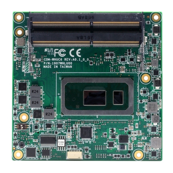
- Page 1 COM-WHUC6 COM Express Module User’s Manual 1 Last Updated: December 20, 2019...
- Page 2 Copyright Notice This document is copyrighted, 2019. All rights are reserved. The original manufacturer reserves the right to make improvements to the products described in this manual at any time without notice. No part of this manual may be reproduced, copied, translated, or transmitted in any form or by any means without the prior written permission of the original manufacturer.
- Page 3 Acknowledgement All other products’ name or trademarks are properties of their respective owners. Microsoft Windows is a registered trademark of Microsoft Corp. ⚫ Intel and Celeron are registered trademarks of Intel Corporation ⚫ Core is a trademark of Intel Corporation ⚫...
- Page 4 Packing List Before setting up your product, please make sure the following items have been shipped: Item Quantity COM-WHUC6 ⚫ If any of these items are missing or damaged, please contact your distributor or sales representative immediately. Preface...
- Page 5 About this Document This User’s Manual contains all the essential information, such as detailed descriptions and explanations on the product’s hardware and software features (if any), its specifications, dimensions, jumper/connector settings/definitions, and driver installation instructions (if any), to facilitate users in setting up their product. Users may refer to the product page at AAEON.com for the latest version of this document.
- Page 6 Safety Precautions Please read the following safety instructions carefully. It is advised that you keep this manual for future references All cautions and warnings on the device should be noted. Make sure the power source matches the power rating of the device. Position the power cord so that people cannot step on it.
- Page 7 If any of the following situations arises, please the contact our service personnel: Damaged power cord or plug Liquid intrusion to the device iii. Exposure to moisture Device is not working as expected or in a manner as described in this manual The device is dropped or damaged Any obvious signs of damage displayed on the device...
- Page 8 FCC Statement This device complies with Part 15 FCC Rules. Operation is subject to the following two conditions: (1) this device may not cause harmful interference, and (2) this device must accept any interference received including interference that may cause undesired operation.
- Page 9 China RoHS Requirements (CN) 产品中有毒有害物质或元素名称及含量 AAEON Main Board/ Daughter Board/ Backplane 有毒有害物质或元素 部件名称 铅 汞 镉 六价铬 多溴联苯 多溴二苯醚 (Pb) (Hg) (Cd) (Cr(VI)) (PBB) (PBDE) 印刷电路板 ○ ○ ○ ○ ○ ○ 及其电子组件 外部信号 ○ ○ ○ ○ ○ ○ 连接器及线材...
- Page 10 China RoHS Requirement (EN) Poisonous or Hazardous Substances or Elements in Products AAEON Main Board/ Daughter Board/ Backplane Poisonous or Hazardous Substances or Elements Hexavalent Polybrominated Polybrominated Component Lead Mercury Cadmium Chromium Biphenyls Diphenyl Ethers (Pb) (Hg) (Cd) (Cr(VI)) (PBB) (PBDE) PCB &...
-
Page 11: Table Of Contents
Table of Contents Chapter 1 - Product Specifications..................1 Specifications ......................2 Chapter 2 – Hardware Information ..................4 Dimensions ....................... 5 Jumpers and Connectors ..................8 List of Jumpers and Switches ................9 2.3.1 AT/ATX Switch & DDI/VGA Switch (SW1) ..........9 List of Connectors .................... - Page 12 System I/O ......................39 3.5.1 PCI Express Configuration................ 40 3.5.1.1 PCI Express Configuration: PCIE_0 ..........41 3.5.1.2 PCI Express Configuration: PCIE_1..........42 3.5.1.3 PCI Express Configuration: PCIE_2 ..........43 3.5.1.4 PCI Express Configuration: PCIE_3 ..........44 3.5.1.5 PCI Express Configuration: PCIE_4 ..........45 3.5.2 Storage Configuration ................
- Page 13 I/O Address Map ....................76 Interrupt Request (IRQ) Address Map ............... 78 Memory Address Map ..................91 Appendix C – Programming Digital I/O................92 Digital I/O Programming ..................93 Digital I/O Register ....................93 Digital I/O Sample Program ................94 Preface XIII...
-
Page 14: Chapter 1 - Product Specifications
Chapter 1 Chapter 1 - Product Specifications... -
Page 15: Specifications
Specifications System Form Factor COM Express Compact size, 95mm x 95mm 8th Generation Intel® Core™ ULT Series Processor CPU Frequency Chipset Onboard 8th Generation Intel® Core™ SoC Memory Type SO-DIMM DDR4 2400 Socket x2 Max. Memory Capacity Up to 32GB BIOS AMI BIOS, Legacy free BIOS Wake on LAN... - Page 16 Display VGA/LCD Controller Intel® UHD Graphics 620 / 610 Video Output DDI0: LVDS, (eDP by BOM change) DDI1: Display Port DDI2: Default VGA, (DP by SW1&2 selected) LVDS Interface Support 18-bit and 24-bit dual channel Ethernet Intel® I219 GbE x 1 Audio HD Audio x 1 USB Port...
-
Page 17: Chapter 2 - Hardware Information
Chapter 2 Chapter 2 – Hardware Information... -
Page 18: Dimensions
Dimensions Chapter 2 – Hardware Information... - Page 19 Chapter 2 – Hardware Information...
- Page 20 With Heat Sink (Part No: COM-WHUC6-HSK01) With Active Cooling (Part No: COM-WHUC6-FAN01) With Heat Spreader and Active Cooling (Part No: COM-WHUC6-HSP01 and COM-FAN02) Chapter 2 – Hardware Information...
-
Page 21: Jumpers And Connectors
Jumpers and Connectors Top Side Bottom Side Chapter 2 – Hardware Information... -
Page 22: List Of Jumpers And Switches
List of Jumpers and Switches Please refer to the table below for all of the board’s jumpers that you can configure for your application Label Function AT/ATX switch & DDI/VGA switch 2.3.1 AT/ATX Switch & DDI/VGA Switch (SW1) AT Mode ATX Mode (Default) VGA (Default) Chapter 2 –... -
Page 23: List Of Connectors
List of Connectors Please refer to the table below for all of the board’s connectors that you can configure for your application Label Function RTC Battery Connector Express ROW A/B Connector Express ROW C/D Connector DDR4 SO-DIMMCOM Connector DDR4 SO-DIMMCOM Connector EC Flash Programming Connector SPI Flash Programming Connector LPC debug card Connector... - Page 24 Row A Row B Signal Signal GBE0_MDI1+ LPC_CLK GND (FIXED) GND (FIXED) GBE0_MDI0- PWRBTN# GBE0_MDI0+ SMB_CK GBE0_CTREF(NC) SMB_DAT SUS_S3# SMB_ALERT# SATA0_TX+ SATA1_TX+ SATA0_TX- SATA1_TX- SUS_S4# SUS_STAT# SATA0_RX+ SATA1_RX+ SATA0_RX- SATA1_RX- GND (FIXED) GND (FIXED) SATA2_TX+ SATA3_TX+(NC) SATA2_TX- SATA3_TX-(NC) SUS_S5# PWR_OK SATA2_RX+ SATA3_RX+(NC) SATA2_RX-...
- Page 25 Row A Row B Signal Signal THRMTRIP# THRM# USB6- USB7- USB6+ USB7+ USB_6_7_OC# USB_4_5_OC# USB4- USB5- USB4+ USB5+ GND (FIXED) GND (FIXED) USB2- USB3- USB2+ USB3+ USB_2_3_OC# USB_0_1_OC# USB0- USB1- USB0+ USB1+ VCC_RTC EXCD1_PERST# EXCD0_PERST# EXCD1_CPPE# (NC) EXCD0_CPPE# (NC) SYS_RESET# LPC_SERIRQ CB_RESET# GND (FIXED)
- Page 26 Row A Row B Signal Signal GND (FIXED) GND (FIXED) PCIE_TX2+ PCIE_RX2+ PCIE_TX2- PCIE_RX2- GPI1 GPO3 PCIE_TX1+ PCIE_RX1+ PCIE_TX1- PCIE_RX1- WAKE0# GPI2 WAKE1# PCIE_TX0+ PCIE_RX0+ PCIE_TX0- PCIE_RX0- GND (FIXED) GND (FIXED) LVDS_A0+ LVDS_B0+ LVDS_A0- LVDS_B0- LVDS_A1+ LVDS_B1+ LVDS_A1- LVDS_B1- LVDS_A2+ LVDS_B2+ LVDS_A2- LVDS_B2-...
- Page 27 Row A Row B Signal Signal GPI3 VCC_5V_SBY RSVD VCC_5V_SBY RSVD VCC_5V_SBY PCIE0_CK_REF+ BISO_DIS1# PCIE0_CK_REF- VGA_RED GND (FIXED) GND (FIXED) SPI _POWER VGA_GRN SPI_MISO VGA_BLU GPO0 VGA_HSYNC SPI_CLK VGA_VSYNC SPI_MOSI VGA_I2C_CK TPM_PP VGA_I2C_DAT TYPE10#(NC) SPI_CS# SER0_TX RSVD SER0_RX RSVD A100 GND (FIXED) B100 GND (FIXED)
-
Page 28: Com Express Row C/D Connector (Cn3)
Row A Row B Signal Signal A110 GND (FIXED) B110 GND (FIXED) 2.4.2 COM Express ROW C/D Connector (CN3) Row C Row D Signal Signal GND (FIXED) GND (FIXED) GND (FIXED) GND (FIXED) USB_SSRX0- USB_SSTX0- USB_SSRX0+ USB_SSTX0+ GND (FIXED) GND (FIXED) USB_SSRX1- USB_SSTX1- USB_SSRX1+... - Page 29 Row C Row D Signal Signal PCIE_RX6- PCIE_TX6- GND (FIXED) GND (FIXED) PCIE_RX7+ PCIE_TX7+ PCIE_RX7- PCIE_TX7- DDI1_HPD RSVD DDI1_PAIR4+(NC) RSVD DDI1_PAIR4-(NC) DDI1_PAIR0+ RSVD DDI1_PAIR0- RSVD RSVD DDI1_PAIR5+(NC) DDI1_PAIR1+ DDI1_PAIR5-(NC) DDI1_PAIR1- GND (FIXED) GND (FIXED) DDI2_CTRLCLK_AUX+ DDI1_PAIR2+ DDI2_CTRLDATA_AUX- DDI1_PAIR2- DDI2_DDC_AUX_SEL DDI1_DDC_AUX_SEL RSVD RSVD DDI3_CTRLCLK_AUX+(NC)
- Page 30 Row C Row D Signal Signal RSVD RSVD DDI3_PAIR2+(NC) DDI2_PAIR2+ DDI3_PAIR2-(NC) DDI2_PAIR2- RSVD RSVD DDI3_PAIR3+(NC) DDI2_PAIR3+ DDI3_PAIR3-(NC) DDI2_PAIR3- GND (FIXED) GND (FIXED) PEG_RX0+(NC) PEG_TX0+(NC) PEG_RX0-(NC) PEG_TX0-(NC) TYPE0#(NC) PEG_LAN_RV#(NC) PEG_RX1+(NC) PEG_TX1+(NC) PEG_RX1-(NC) PEG_TX1-(NC) TYPE1#(NC) TYPE2# PEG_RX2+(NC) PEG_TX2+(NC) PEG_RX2-(NC) PEG_TX2-(NC) GND (FIXED) GND (FIXED) PEG_RX3+(NC) PEG_TX3+(NC)
- Page 31 Row C Row D Signal Signal GND (FIXED) GND (FIXED) PEG_RX6+(NC) PEG_TX6+(NC) PEG_RX6-(NC) PEG_TX6-(NC) GND (FIXED) GND (FIXED) PEG_RX7+(NC) PEG_TX7+(NC) PEG_RX7-(NC) PEG_TX7-(NC) GND (FIXED) GND (FIXED) RSVD RSVD PEG_RX8+(NC) PEG_TX8+(NC) PEG_RX8-(NC) PEG_TX8-(NC) GND (FIXED) GND (FIXED) PEG_RX9+(NC) PEG_TX9+(NC) PEG_RX9-(NC) PEG_TX9-(NC) RSVD RSVD GND (FIXED)
- Page 32 Row C Row D Signal Signal PEG_RX13-(NC) PEG_TX13-(NC) GND (FIXED) GND (FIXED) RSVD RSVD PEG_RX14+(NC) PEG_TX14+(NC) PEG_RX14-(NC) PEG_TX14-(NC) C100 GND (FIXED) D100 GND (FIXED) C101 PEG_RX15+(NC) D101 PEG_TX15+(NC) C102 PEG_RX15-(NC) D102 PEG_TX15-(NC) C103 GND (FIXED) D103 C104 VCC_12V D104 VCC_12V C105 VCC_12V D105...
-
Page 33: Function Block Diagram
Function Block Diagram Chapter 2 – Hardware Information... -
Page 34: Chapter 3 - Ami Bios Setup
Chapter 3 Chapter 3 - AMI BIOS Setup... -
Page 35: System Test And Initialization
System Test and Initialization The board uses certain routines to test and initialize board hardware. If the routines encounter an error during the tests, you will either hear a few short beeps or see an error message on the screen. There are two kinds of errors: fatal and non-fatal. The system can usually continue the boot up sequence with non-fatal errors. -
Page 36: Ami Bios Setup
AMI BIOS Setup The AMI BIOS ROM has a built-in Setup program that allows users to modify the basic system configuration. This information is stored in the battery-backed CMOS RAM and BIOS NVRAM so it retains the Setup information when the power is turned off. To enter Setup, power on the computer and press <Del>... -
Page 37: Main
Main Chapter 3 – AMI BIOS Setup... -
Page 38: Advanced
Advanced Chapter 3 – AMI BIOS Setup... -
Page 39: Graphics Configuration
3.4.1 Graphics Configuration Options Summary Skip Scaning of Disabled Optimal Default, Failsafe Default External Gfx Card Enabled If Enable, it will not scan for External Gfx Card on PEG and PCH PCIE Ports Primary Display Auto Optimal Default, Failsafe Default IGFX Select which of TGFX/PEG/PCI Graphics device should be Primary Display Or select SG for Switchable Gfx. - Page 40 Options Summary DVMT Pre-Allocated 32M/F7 Select DVMT 5.0 Pre-Allocated (Fixed) Graphics Memory size used by the Internal Graphics Drvice. DVMT Total Gfx 128M 256M Optimal Default, Failsafe Default Select DVMT5.0 Total Graphic Memory Size used by the Internal Graphics Device. Chapter 3 –...
-
Page 41: Lvds Panel Configuration
3.4.2 LVDS Panel Configuration Options Summary Panel Type 640x480@60Hz 800x480@60Hz 800x600@60Hz 1024x600@60Hz 1024x768@60Hz Optimal Default, Failsafe Default 1280x768@60Hz 1280x800@60Hz 1280x1024@60Hz 1366x768@60Hz 1440x900@60Hz 1600x1200@60Hz 1920x1080@60Hz 1920x1200@60Hz Select panel type Chapter 3 – AMI BIOS Setup... - Page 42 Options Summary Color Depth 18-Bit Optimal Default, Failsafe Default 24-Bit 36-Bit 48-Bit Select panel type Backlight Type Normal Optimal Default, Failsafe Default Inverted Select backlight control signal type Backlight Level Optimal Default, Failsafe Default 100% Select backlight control level Backlight PWM Freq 100Hz 200Hz 220Hz Optimal Default, Failsafe Default...
-
Page 43: Cpu Configuration
3.4.3 CPU Configuration Options Summary Active Processor Cores Optimal Default, Failsafe Default Number of cores to enable in each processor package. Hyper-Threading Disabled Enabled Optimal Default, Failsafe Default Enabled or Disabled Hyper-Threading Technology. Intel Trusted Execution Disabled Optimal Default, Failsafe Default Technology Enabled Enables utilization of additional hardware capabilities provided by Intel (R) Trusted... - Page 44 Options Summary Intel (VMX) Virtualization Disabled Technology Enabled Optimal Default, Failsafe Default When enabled, a VMM can utilize the additional hardware capabilities provided by Vanderpool Technology. Intel(R) SpeedStep(tm) Disabled Enabled Optimal Default, Failsafe Default Allows more than two frequency ranges to be supported. Turbo Mode Disabled Enabled...
-
Page 45: Memory Configuration
3.4.4 Memory Configuration Chapter 3 – AMI BIOS Setup... -
Page 46: On-Module H/W Monitor
3.4.5 On-Module H/W Monitor Chapter 3 – AMI BIOS Setup... -
Page 47: Fan 1 Mode Configuration
3.4.5.1 Fan 1 Mode Configuration Options Summary CPU Smart Fan Full Mode Optimal Default, Failsafe Default control Manual Mode by PWM Auto Mode by PWM PWM signa Non-inverting Optimal Default, Failsafe Default Inverting Select output PWM of inverting or non-inverting signal Chapter 3 –... -
Page 48: Pch-Fw Configuration
3.4.6 PCH-FW Configuration Chapter 3 – AMI BIOS Setup... -
Page 49: Firmware Update Configuration
3.4.6.1 Firmware Update Configuration Options Summary Me FW Image Disabled Optimal Default, Failsafe Default Re-Flash Enabled Enable/ Disable Me FW Image Re-Flash Function. Local FW Update Disabled Enabled Optimal Default, Failsafe Default Options for Local FW Update function Chapter 3 – AMI BIOS Setup... -
Page 50: On-Module Configuration
3.4.7 On-Module Configuration Options Summary Battery Managerment Disabled Optimal Default, Failsafe Default One Battery Enable to support battery in ACPI OS by I2C_CK, I2C_DAT(B33,B34) EC-SMB-HC Support Disabled Optimal Default, Failsafe Default Enabled SMBus Host Controller Interface via Embedded Controller. Chapter 3 – AMI BIOS Setup... -
Page 51: Power Management
3.4.8 Power Management Options Summary Power Mode ATX Type AT Type Optimal Default, Failsafe Default Select system power mode. Restore AC Power Loss Last State Always On Always Off Optimal Default, Failsafe Default IO Restore AC Power Loss RTC wake system from S5 Disabled Optimal Default, Failsafe Default Fixed Time Fixed Time: System will wake on the hr::mn::sec Specified. -
Page 52: System I/O
System I/O Chapter 3 – AMI BIOS Setup... -
Page 53: Pci Express Configuration
3.5.1 PCI Express Configuration Options Summary PCIE_0~3 Configuration As four x1 Optimal Default, Failsafe Default As one x2 and two x1 As two x2 As one x4 PCIE Controller Selection PCIE_4~7 Configuration As four x1 As one x2 and two x1 As two x2 As one x4 Optimal Default, Failsafe Default... -
Page 54: Pci Express Configuration: Pcie_0
3.5.1.1 PCI Express Configuration: PCIE_0 Options Summary PCIE_0 Disabled Enabled Optimal Default, Failsafe Default Control the PCI Express Root Port. PCIe Speed Auto Optimal Default, Failsafe Default Gen1 Gen2 Gen3 Configure PCIe Speed Chapter 3 – AMI BIOS Setup... -
Page 55: Pci Express Configuration: Pcie_1
3.5.1.2 PCI Express Configuration: PCIE_1 Options Summary PCIE_1 Disabled Enabled Optimal Default, Failsafe Default Control the PCI Express Root Port. PCIe Speed Auto Optimal Default, Failsafe Default Gen1 Gen2 Gen3 Configure PCIe Speed Chapter 3 – AMI BIOS Setup... -
Page 56: Pci Express Configuration: Pcie_2
3.5.1.3 PCI Express Configuration: PCIE_2 Options Summary PCIE_2 Disabled Enabled Optimal Default, Failsafe Default Control the PCI Express Root Port. PCIe Speed Auto Optimal Default, Failsafe Default Gen1 Gen2 Gen3 Configure PCIe Speed Chapter 3 – AMI BIOS Setup... -
Page 57: Pci Express Configuration: Pcie_3
3.5.1.4 PCI Express Configuration: PCIE_3 Options Summary PCIE_3 Disabled Enabled Optimal Default, Failsafe Default Control the PCI Express Root Port. PCIe Speed Auto Optimal Default, Failsafe Default Gen1 Gen2 Gen3 Configure PCIe Speed Chapter 3 – AMI BIOS Setup... -
Page 58: Pci Express Configuration: Pcie_4
3.5.1.5 PCI Express Configuration: PCIE_4 Options Summary PCIE_4 Disabled Enabled Optimal Default, Failsafe Default Control the PCI Express Root Port. PCIe Speed Auto Optimal Default, Failsafe Default Gen1 Gen2 Gen3 Configure PCIe Speed Chapter 3 – AMI BIOS Setup... -
Page 59: Storage Configuration
3.5.2 Storage Configuration Options Summary eMMC 5.0 Disabled Controller Enabled Optimal Default, Failsafe Default Enable or Disable SCS eMMC 5.0 Controller eMMC 5.0 HS400 Disabled Mode Enabled Optimal Default, Failsafe Default Enable or Disable SCS eMMC 5.0 HS400 Mode Driver Strength 33 Ohm 40 Ohm Optimal Default, Failsafe Default... - Page 60 Options Summary SATA Mode AHCI Optimal Default, Failsafe Default Selection Intel RST Premium with Intel Optane System Acceleration Determines how SATA controller(s) operate. Port 0 Disabled Enabled Optimal Default, Failsafe Default Enabled or Disabled SATA Port Hot Plug Disabled Optimal Default, Failsafe Default Enabled Designates this port as Hot Pluggable.
-
Page 61: Hd Audio Configuration
3.5.3 HD Audio Configuration Options Summary HD Audio Disabled Enabled Optimal Default, Failsafe Default Control Detection of the HD-Audio device. Disabled = HDA will be unconditionally disabled Enabled = HDA will be unconditionally enabled. Chapter 3 – AMI BIOS Setup... -
Page 62: Digital Io Port Configuration
3.5.4 Digital IO Port Configuration Options Summary GPI0 Input Optimal Default, Failsafe Default Output Set DIO as Input or Output GPI1 Input Optimal Default, Failsafe Default Output Set DIO as Input or Output GPI2 Input Optimal Default, Failsafe Default Output Set DIO as Input or Output GPI3 Input... - Page 63 Options Summary Output Level High Optimal Default, Failsafe Default Set output level when DIO pin is output GPO1 Input Output Optimal Default, Failsafe Default Set DIO as Input or Output Output Level High Optimal Default, Failsafe Default Set output level when DIO pin is output GPO2 Input Output...
-
Page 64: Sio Configuration
3.5.5 SIO Configuration Chapter 3 – AMI BIOS Setup... -
Page 65: Serial Port 1 Configuration
3.5.5.1 Serial Port 1 Configuration Options Summary Use This Device Disabled Enabled Optimal Default, Failsafe Default Enable or Disable this Logical Device. Possible: Use Automatic Settings Optimal Default, Failsafe Default IO=3F8h; IRQ=4; DMA; IO=2C8h; IRQ=11; DMA; Allows the user to change the device resource settings. New settings will be reflected on this setup page after system restarts. -
Page 66: Serial Port 2 Configuration
3.5.5.2 Serial Port 2 Configuration Options Summary Use This Device Disabled Enabled Optimal Default, Failsafe Default Enable or Disable this Logical Device. Possible: Use Automatic Settings Optimal Default, Failsafe Default IO=2F8h; IRQ=3 DMA; IO=2D8h; IRQ=10; DMA; Allows the user to change the device resource settings. New settings will be reflected on this setup page after system restarts. -
Page 67: Serial Port Console Redirection
3.5.6 Serial Port Console Redirection Options Summary Console Redirection Disabled Optimal Default, Failsafe Default Enabled Console Redirection Enable or Disable. Console Redirection Disabled Optimal Default, Failsafe Default Enabled Console Redirection Enable or Disable. Chapter 3 – AMI BIOS Setup... -
Page 68: Legacy Console Redirection Settings
3.5.6.1 Legacy Console Redirection Settings Options Summary Redirection COM Port COM0 Optimal Default, Failsafe Default Select a COM port to display redirection of Legacy OS and Legacy OPROM Messages Resolution 80x24 Optimal Default, Failsafe Default 80x25 On Legacy OS, the Number of Rows and Columns supported redirection Redirect After POST Always Enable Optimal Default, Failsafe Default... -
Page 69: Ram Disk Configuration
3.5.7 RAM Disk Configuration Options Summary Disk Memory Type: Boot Service Data Optimal Default, Failsafe Default Reserved Specifies type of memory to use from available memory pool in system to create a disk. Create from file HDD Unknown 96MB Optimal Default, Failsafe Default Create a RAM disk from a given file. -
Page 70: Ram Disk Configurator: Create Raw
3.5.7.1 RAM Disk Configurator: Create Raw Options Summary Size (Hex) Optimal Default, Failsafe Default The valid RAM disk size should be multiples of the RAM disk block size. Create & Exit Create a new RAM disk with the given starting and ending address. Discard &... -
Page 71: Security
Security Change Administrator/User Password You can set an Administrator password. If you set an Administrator password, you can then set a User password. User passwords do not have access to many of the features in the Setup utility. Select the password you want to set and press <Enter>. A dialog box will appear which lets you set the password. -
Page 72: Security: Secure Boot
3.6.1 Security: Secure Boot Options Summary Secure Boot Disabled Optimal Default, Failsafe Default Enabled Secure Boot feature is Active if Secure Boot is Enabled, Platform Key (PK) is enrolled and the System is in User mode. The mode change requires platform reset Secure Boot Mode Standard Custom... -
Page 73: Secure Boot: Key Management
3.6.1.1 Secure Boot: Key Management Options Summary Factory Key Provision Disabled Optimal Default, Failsafe Default Enabled Install factory default Secure Boot keys after the platform reset and while the System is in Setup mode Restore Factory Keys Yes Optimal Default, Failsafe Default Force System to User Mode. - Page 74 Options Summary Restore DB defaults Yes Optimal Default, Failsafe Default Restore DB variable to factory defaults Platform Key(PK) | 0| Update Optimal Default, Failsafe Default 0| No Keys Key Exchange Keys| Update Optimal Default, Failsafe Default 0| 0| No Keys Append Authorized Update...
-
Page 75: Trusted Computing
3.6.2 Trusted Computing Options Summary Security Device Disable Support Enable Optimal Default, Failsafe Default Enables or Disables BIOS support for security device. O.S. will not show Security Device. TCG EFI protocol and INT1A interface will not be available. TPM State Disable Enable Optimal Default, Failsafe Default... - Page 76 Options Summary Device Select TPM 1.2 TPM 2.0 Auto Optimal Default, Failsafe Default TPM 1.2 will restrict support to TPM 1.2 Devices, TPM 2.0 will restrict support to TPM 2.0 devices, Auto will support both with the default set to TPM 2.0 devices if not found, TPM 1.2 devices will be enumerated Chapter 3 –...
-
Page 77: Setup Submenu: Boot
Setup submenu: Boot Options Summary Quiet Boot Disabled Enabled Optimal Default, Failsafe Default Restore DB variable to factory defaults PXE Boot Disabled Optimal Default, Failsafe Default UEFI Controls the execution of UEFI and Legacy Network OpROM Chapter 3 – AMI BIOS Setup... -
Page 78: Setup Submenu: Save & Exit
Setup submenu: Save & Exit Chapter 3 – AMI BIOS Setup... -
Page 79: Chapter 4 - Drivers Installation
Chapter 4 Chapter 4 – Drivers Installation... -
Page 80: Drivers Download And Installation
Drivers Download and Installation Drivers for the COM-WHUC6 can be downloaded from the product page on the AAEON website by following this link: https://www.aaeon.com/en/p/com-express-modules-com-whuc6 Download the driver(s) you need and follow the steps below to install them. Step 1 – Install Chipset Driver Click the STEP1 - Chipset folder. - Page 81 Step 4 – Install Audio Driver Click the STEP4 - Audio folder. Open the 0006-64bit_Win7_Win8_Win81_Win10_R279.exe file. Follow the instructions Drivers will be installed automatically Step 5 – Install Intel Management Engine Driver Click the STEP5 – Intel Management Engine then open folder for your OS. 2.
-
Page 82: Appendix A - Watchdog Timer
Appendix A Appendix A - Watchdog Timer... -
Page 83: Watchdog Timer Initial Program
Watchdog Timer Initial Program Table 1: Embedded BRAM relative register table Default Value Note Index 0x284(Note1) BRAM Index Register Data 0x285(Note2) BRAM Data Register Logical Device Number 0xA8(Note3) Watch dog Logical Device Number Function and Device Number 0x00(Note4) Watch dog Function/Device Number Table 2: Watchdog relative register table Option BitNum... - Page 84 ************************************************************************************ // Embedded BRAM relative definition (Please reference to Table 1) #define byte EcBRAMIndex //This parameter is represented from Note1 #define byte EcBRAMData //This parameter is represented from Note2 #define byte BRAMLDNReg //This parameter is represented from Note3 #define byte BRAMFnDataReg //This parameter is represented from Note4 #define void EcBRAMWriteByte(byte Offset, byte Value);...
- Page 85 ************************************************************************************ Main VOID // Procedure : AaeonWDTConfig // (byte)Timer : Time of WDT timer.(0x00~0xFF) // (boolean)Unit : Select time unit(0: second, 1: minute). AaeonWDTConfig(); // Procedure : AaeonWDTEnable // This procudure will enable the WDT counting. AaeonWDTEnable(); ************************************************************************************ Appendix A – Watchdog Timer Programming...
- Page 86 ************************************************************************************ // Procedure : AaeonWDTEnable AaeonWDTEnable () VOID WDTEnableDisable( // Procedure : AaeonWDTConfig AaeonWDTConfig () VOID // Disable WDT counting WDTEnableDisable( // WDT relative parameter setting WDTParameterSetting(); WDTEnableDisable(byte Value) VOID ECBRAMWriteByte(TimerReg , Value); WDTParameterSetting() VOID Byte TempByte; // Watchdog Timer counter setting ECBRAMWriteByte(TimerReg , TimerVal);...
- Page 87 ************************************************************************************ ECBRAMWriteByte(byte OPReg, byte OPBit, byte Value) VOID IOWriteByte(EcBRAMIndex, 0x10); IOWriteByte(EcBRAMData, BRAMLDNReg); IOWriteByte(EcBRAMIndex, 0x11); IOWriteByte(EcBRAMData, BRAMFnDataReg); IOWriteByte(EcBRAMIndex, 0x13 + OPReg); IOWriteByte(EcBRAMData, Value); IOWriteByte(EcBRAMIndex, 0x12); IOWriteByte(EcBRAMData, 0x30); //Write start ECBRAMReadByte(byte OPReg) Byte IOWriteByte(EcBRAMIndex, 0x10); IOWriteByte(EcBRAMData, BRAMLDNReg); IOWriteByte(EcBRAMIndex, 0x11); IOWriteByte(EcBRAMData, BRAMFnDataReg); IOWriteByte(EcBRAMIndex, 0x12); IOWriteByte(EcBRAMData, 0x10);...
-
Page 88: Appendix B - I/O Information
Appendix B Appendix B - I/O Information... -
Page 89: I/O Address Map
I/O Address Map Appendix B – I/O Information... - Page 90 Appendix B – I/O Information...
-
Page 91: Interrupt Request (Irq) Address Map
Interrupt Request (IRQ) Address Map Appendix B – I/O Information... - Page 92 Appendix B – I/O Information...
- Page 93 Appendix B – I/O Information...
- Page 94 Appendix B – I/O Information...
- Page 95 Appendix B – I/O Information...
- Page 96 Appendix B – I/O Information...
- Page 97 Appendix B – I/O Information...
- Page 98 Appendix B – I/O Information...
- Page 99 Appendix B – I/O Information...
- Page 100 Appendix B – I/O Information...
- Page 101 Appendix B – I/O Information...
- Page 102 Appendix B – I/O Information...
- Page 103 Appendix B – I/O Information...
-
Page 104: Memory Address Map
Memory Address Map Appendix B – I/O Information... -
Page 105: Appendix C - Programming Digital I/O
Appendix C Appendix C – Programming Digital I/O... -
Page 106: Digital I/O Programming
Digital I/O Programming The COM-WHUC6 utilizes an AAEON chipset as its Digital I/O controller. Below are the procedures to complete its configuration, which you can use to develop a customized program to fit your application. C.2 Digital I/O Register Table 1: Embedded BRAM relative register table Default Value Note Index... -
Page 107: C.3 Digital I/O Sample Program
C.3 Digital I/O Sample Program ************************************************************************************ // Embedded BRAM relative definition (Please reference to Table 1) #define byte EcBRAMIndex //This parameter is represented from Note1 #define byte EcBRAMData //This parameter is represented from Note2 #define byte BRAMLDNReg //This parameter is represented from Note3 #define byte BRAMFnData0Reg //This parameter is represented from Note4... - Page 108 ************************************************************************************ Main VOID Boolean PinStatus ; // Procedure : AaeonReadPinStatus // Input : Example, Read Digital I/O Pin 3 status // Output : InputStatus : 0: Digital I/O Pin level is low 1: Digital I/O Pin level is High PinStatus = AaeonReadPinStatus(DIO0ToDIO7Reg, DIO3Bit); // Procedure : AaeonSetOutputLevel // Input : Example, Set Digital I/O Pin 6 level...
- Page 109 ************************************************************************************ AaeonReadPinStatus(byte OptionReg, byte BitNum) Boolean Byte TempByte; TempByte = ECBRAMReadByte(BRAMFnData1Reg, OptionReg); If (TempByte & BitNum == 0) Return 0; Return 1; AaeonSetOutputLevel(byte OptionReg, byte BitNum, byte Value) VOID Byte TempByte; TempByte = ECBRAMReadByte(BRAMFnData1Reg, OptionReg); TempByte |= (Value << BitNum); ECBRAMWriteByte(OptionReg, BitNum, Value);...
- Page 110 ************************************************************************************ ECBRAMWriteByte(byte OPReg, byte OPBit, byte Value) VOID IOWriteByte(EcBRAMIndex, 0x10); IOWriteByte(EcBRAMData, BRAMLDNReg); IOWriteByte(EcBRAMIndex, 0x11); IOWriteByte(EcBRAMData, BRAMFnDataReg); IOWriteByte(EcBRAMIndex, 0x13 + OPReg); IOWriteByte(EcBRAMData, Value); IOWriteByte(EcBRAMIndex, 0x12); IOWriteByte(EcBRAMData, 0x30); //Write start ECBRAMReadByte(byte FnDataReg, byte OPReg) Byte IOWriteByte(EcBRAMIndex, 0x10); IOWriteByte(EcBRAMData, BRAMLDNReg); IOWriteByte(EcBRAMIndex, 0x11); IOWriteByte(EcBRAMData, FnDataReg); IOWriteByte(EcBRAMIndex, 0x12);...