
Related Manuals for Motorola 700 Series


Summary of Contents for Motorola 700 Series
- Page 1 700/800-Series MVME162LX Embedded Controller Installation and Use 700/800-Series MVME162LX Embedded Controller Installation and Use...
- Page 3 700/800-Series MVME162LX Embedded Controller Installation and Use V162-7A/IH1...
- Page 4 Motorola, Inc. assumes no liability resulting from any omissions in this document, or from the use of the information obtained therein. Motorola reserves the right to revise this document and to make changes from time to time in the content hereof without obligation of Motorola to notify any person of such revision or changes.
- Page 5 Preface This document provides general information and basic installation instructions for the 700/800-series MVME162LX VME Embedded Controller, which is available in the versions listed below. Assembly Board Assembly Item Board Description Item Description MVME162-723 32MHz, 4MB DRAM MVME162-813 32MHz, 8MB DRAM MVME162-743 32MHz, 4MB ECC...
- Page 6 Motorola, Inc. assumes no liability for the customer's failure to comply with these requirements. The safety precautions listed below represent warnings of certain dangers of which Motorola is aware. You, as the user of the product, should follow these warnings and all other safety precautions necessary for the safe operation of the equipment in your operating environment.
- Page 7 Lithium Battery Caution The board contains a lithium battery to power the clock and calendar circuitry. Danger of explosion if battery is replaced incorrectly. Replace only with the same or equivalent type recommended by the equipment manufacturer. Dispose CAUTION of used batteries according to the manufacturer’s instructions.
- Page 8 CE-marked system will maintain the required EMC/safety performance. The computer programs stored in the Read Only Memory of this device contain material copyrighted by Motorola Inc., 1995, and may be used only under a license such as those contained in Motorola’s software licenses. ®...
-
Page 9: Table Of Contents
Chapter 1 Board Level Hardware Description Introduction ......................1-1 Overview......................1-1 Related Documentation ................1-3 Documents for the MVME162LX ..............1-4 Other Applicable Motorola Publications ........... 1-4 Applicable Non-Motorola Publications ............. 1-5 Requirements....................1-6 Features ......................1-6 Specifications....................1-8 Cooling Requirements .................. 1-9 Special Considerations for Elevated-Temperature Operation ....1-9 FCC Compliance.................. - Page 10 Chapter 1 Board Level Hardware Description continued Optional SCSI Interface................ 1-23 SCSI Termination .................. 1-23 Local Resources ................... 1-24 Programmable Tick Timers ..............1-24 Watchdog Timer ................... 1-24 Software-Programmable Hardware Interrupts........ 1-25 Local Bus Timeout ................1-25 Local Bus Arbiter..................1-26 Connectors....................
- Page 11 Chapter 3 Debugger General Information Overview of M68000 Firmware................3-1 Description of 162Bug ..................3-1 162Bug Implementation ..................3-3 Installation and Startup..................3-3 Prom Versions ....................3-7 Autoboot........................3-7 ROMboot .......................3-9 Network Boot......................3-10 Restarting the System ..................3-10 Reset....................... 3-11 Abort......................3-11 Break ......................3-12 SYSFAIL* Assertion/Negation ..............
- Page 12 Chapter 3 Debugger General Information continued Multiprocessor Support ..................3-22 Multiprocessor Control Register (MPCR) Method......... 3-22 GCSR Method ....................3-24 Diagnostic Facilities................... 3-25 Manufacturing Test Process................3-25 Chapter 4 Using the 162Bug Debugger In This Chapter..................... 4-1 Entering Debugger Command Lines ..............4-1 Terminal Input/Output Control ..............
- Page 13 Appendix A Configure and Environment Commands Configure Board Information Block ..............A-1 Set Environment to Bug/Operating System ...........A-3 Configuring the IndustryPacks ..............A-14 Appendix B Disk/Tape Controller Data Disk/Tape Controller Modules Supported ............B-1 Disk/Tape Controller Default Configurations..........B-2 IOT Command Parameters for Supported Floppy Types ......B-4 Appendix C Network Controller Data Network Controller Modules Supported ............
- Page 14 Figures Figure 1-1. MVME162LX Block Diagram ............1-14 Figure 2-1. MVME162LX Board Layout............2-4 Figure 2-2. DB-25 DTE-to-RJ-45 Adapter............2-20 Figure 2-3. DB-25 DCE-to-RJ-45 Adapter ............2-20 Figure 2-4. Typical RJ-45 Serial Cable............. 2-21 Tables Table 1-1. 700/800-Series MVME162LX: Features........... 1-6 Table 1-2.
-
Page 15: Introduction
1Board Level Hardware Description Introduction This chapter describes the board level hardware features of the 700/800-series MVME162LX VME Embedded Controller. The chapter is organized with a board level overview and features list in this introduction, followed by a more detailed hardware functional description. - Page 16 Board Level Hardware Description connector, and four 8-pin RJ-45 serial connectors on the front panel. In addition, the panel has cutouts for routing of flat cables to the optional IndustryPack modules. The following ASICs are used on the MVME162LX: VMEchip2. (VMEbus interface). Provides two tick timers, a watchdog timer, programmable map decoders for the master and slave interfaces, and a VMEbus to/from local bus DMA controller, a VMEbus to/from local bus non-DMA...
-
Page 17: Related Documentation
If you plan to develop your own applications or need more detailed information about your MVME162LX VME Embedded Controller, you may wish to order the additional documentation listed on the following pages. You can contact Motorola for this purpose in several ways: Through your local Motorola sales office... -
Page 18: Documents For The Mvme162Lx
Single Board Computers SCSI Software User’s Manual Other Applicable Motorola Publications The following publications are also applicable to the 700/800-series MVME162LX and may provide additional helpful information. They may be purchased through your local Motorola sales office. Motorola Description Publication Number... -
Page 19: Applicable Non-Motorola Publications
Introduction Applicable Non-Motorola Publications The following non-Motorola publications are also available from the sources indicated. Document Title Source VME64 Specification, order number VITA (VMEbus International ANSI/VITA 1-1994 Trade Association) 7825 E. Gelding Dr., Ste. 104 Scottsdale, AZ 85260-3415 Note: An earlier version of the VME specification is available as Versatile Backplane... -
Page 20: Requirements
Board Level Hardware Description Document Title Source IndustryPack Logic Interface Specification, VITA (VMEbus International Revision 1.0, order number ANSI/VITA 4-1995 Trade Association) 7825 E. Gelding Dr., Ste. 104 Scottsdale, AZ 85260-3415 Z85230 Serial Communications Controller Data Zilog Inc. Sheet 210 Hacienda Ave. Campbell, CA 95008-6609 Requirements These boards are designed to conform to the requirements of the... - Page 21 Introduction Table 1-1. 700/800-Series MVME162LX: Features (Continued) Feature Description 8K by 8 Non-Volatile RAM (NVRAM) and time-of-day NVRAM (TOD) clock with battery backup switches Switches RESET ABORT Status LEDs Status LEDs for , and FAIL SCON FUSES Four 32-bit tick timers (in the MC2chip ASIC); two 32-bit Tick Timers tick timers (in the VMEchip2 ASIC) for periodic interrupts in the MC2chip and...
-
Page 22: Specifications
Board Level Hardware Description Specifications Table 1-2 lists the specifications for a 700/800-series MVME162LX without IPs. Table 1-2. 700/800-Series MVME162LX: Specifications Characteristics Specifications Power requirements +5Vdc ( 5%), 3.5 A typical, 4.5 A maximum (with EPROMs; without IPs) +12 Vdc ( 5%), 100 mA maximum -12 Vdc ( 5%), 100 mA maximum Operating temperature 0˚... -
Page 23: Cooling Requirements
0˚ to 55˚ C (32˚ to 131˚ F) with forced air cooling at a velocity typically achievable by using a 100 CFM axial fan. Temperature qualification is performed in a standard Motorola VME system chassis. Load boards are inserted adjacent to the board under test, to simulate a high power density system configuration. - Page 24 Board Level Hardware Description The MVME162LX uses commercial-grade devices. Therefore, it can operate in an environment with ambient air temperatures from 0˚ C to 70˚ C. Several factors influence the ambient temperature seen by components on the MVME162LX. Among them are inlet air temperature;...
-
Page 25: Fcc Compliance
Introduction FCC Compliance The MVME162LX is a board-level product and is meant to be used in standard VME applications. As such, it is the responsibility of system integrators to to meet the regulatory guidelines pertaining to a given application. The MVME162LX has been tested in a representative chassis for CE class B EMC certification. - Page 26 Board Level Hardware Description An asterisk (*) following the signal name for signals which are level significant denotes that the signal is true or valid when the signal is low. An asterisk (*) following the signal name for signals which are edge significant denotes that the actions initiated by that signal occur on high-to-low transition.
-
Page 27: Block Diagram
Block Diagram Block Diagram Refer to Figure 1-1 on page 1-14 for a block diagram of the 700/800- series MVME162LX. Functional Description This section contains a functional description of the major blocks on the MVME162LX. Front Panel Switches and Indicators There are two switches and four LEDs on the front panel of the MVME162LX. -
Page 28: Figure 1-1. Mvme162Lx Block Diagram
Board Level Hardware Description Figure 1-1. MVME162LX Block Diagram 1-14... -
Page 29: Data Bus Structure
Block Diagram Data Bus Structure The local bus on the MVME162LX is a 32-bit synchronous bus that is based on the MC68040 bus, and which supports burst transfers and snooping. The various local bus master and slave devices use the local bus to communicate. The local bus is arbitrated by priority type arbiter and the priority of the local bus masters from highest to lowest is: 82596CA LAN, 53C710 SCSI, VMEbus, and MPU. -
Page 30: No-Vmebus-Interface Option
162Bug package, MVME162Bug, be sure that jumper header J21 is configured for the EPROM memory map. Refer to Chapters 2 and 3 for further details. Contact your local Motorola sales office for ordering information. Memory Options The following memory options are used on the different versions of 700/800-series MVME162LX boards. -
Page 31: Sram Options
Block Diagram DRAM performance is specified in the section on the DRAM Memory Controller in the MC2chip Programming Model in the MVME162LX Embedded Controller Programmer’s Reference Guide. The DRAM map decoder may be programmed to accommodate different base address(es) and sizes of mezzanine boards. The onboard DRAM is disabled by a local bus reset and must be programmed before the DRAM may be accessed. -
Page 32: About The Battery
Board Level Hardware Description VMEbus +5V STDBY pin and the secondary source may be the onboard battery. If the system source should fail or the board is removed from the chassis, the onboard battery takes over. Refer to Chapter 2 for the jumper configurations. For proper operation of the SRAM, some jumper combination must be installed on the respective Backup Power Source Select Header (J14). - Page 33 Block Diagram battery as a power source, whether primary or secondary, it is necessary to reconfigure the jumpers on J14 before installing the board. Refer to SRAM Backup Power Source Select Header (J14) on page 2-6 for available jumper configurations The power leads from the battery are exposed on the solder side of the board.
-
Page 34: Eprom And Flash Memory
Board Level Hardware Description EPROM and Flash Memory The MVME162LX may be ordered with 2MB of Flash memory and two EPROM sockets ready for the installation of the EPROMs, which may be ordered separately. Flash memory is a single Intel 28F016SA device organized in a 2Mbit x 8 configuration. -
Page 35: I/O Interfaces
Block Diagram Note that the switch logic in the VMEchip2 is not used. The ABORT GPI inputs to the VMEchip2 which are located at $FFF40088 bits 7- 0 are not used. The switch interrupt is integrated into the ABORT MC2chip ASIC at location $FFF42043. The GPI inputs are integrated into the MC2chip ASIC at location $FFF4202C bits 23-16. -
Page 36: Industrypack (Ip) Interfaces
Board Level Hardware Description IndustryPack (IP) Interfaces Up to two IP modules may be installed on the 700/800-series MVME162LX as an option. The interface between the IPs and MVME162LX is the IndustryPack Interface Controller (IP2) ASIC. Access to the IPs is provided by two 3M connectors located behind the MVME162LX front panel. -
Page 37: Optional Scsi Interface
Block Diagram Support functions for the 82596CA are provided by the MC2chip. Refer to the 82596CA user's guide and to the MC2chip description in the MVME162LX Embedded Controller Programmer’s Reference Guide for detailed programming information. Optional SCSI Interface The MVME162LX supports mass storage subsystems through the industry-standard SCSI bus. -
Page 38: Local Resources
Board Level Hardware Description Local Resources The MVME162LX includes many resources for the local processor. These include tick timers, software-programmable hardware interrupts, watchdog timer, and local bus timeout. Programmable Tick Timers Six 32-bit programmable tick timers with 1µs resolution are provided, four in the MC2chip and two in the optional VMEchip2. -
Page 39: Software-Programmable Hardware Interrupts
Block Diagram Software-Programmable Hardware Interrupts Eight software-programmable hardware interrupts are provided by the VMEchip2. These interrupts allow software to create a hardware interrupt. Refer to the VMEchip2 description in the MVME162LX Embedded Controller Programmer’s Reference Guide for detailed programming information. Local Bus Timeout The MVME162LX provides a timeout function in the VMEchip2 and the MC2chip for the local bus. -
Page 40: Local Bus Arbiter
Board Level Hardware Description Local Bus Arbiter The local bus arbiter implements a fixed priority, which is described in the following table. Table 1-3. Local Bus Arbitration Priority Device Priority Note Highest IndustryPack DMA SCSI . . . VMEbus Next lowest MC68040 Connectors The MVME162LX has two 96-position DIN connectors: P1 and P2. -
Page 41: Memory Maps
Memory Maps Memory Maps There are two points of view for memory maps: 1) the mapping of all resources as viewed by local bus masters (local bus memory map), and 2) the mapping of onboard resources as viewed by external masters (VMEbus memory map). The memory and I/O maps that are described in the next three tables are correct for all local bus masters. -
Page 42: Table 1-4. Local Bus Memory Map
Board Level Hardware Description I/O space must be marked cache inhibit and serialized in its page table. Table 1-5 on page 1-30 further defines the map for the local I/O devices. Table 1-4. Local Bus Memory Map Software Devices Port Address Range Size Cache... - Page 43 Memory Maps Table 1-4. Local Bus Memory Map (Continued) Software Devices Port Address Range Size Cache Notes Accessed Width Inhibit $FFE80000-$FFEFFFFF Not decoded 512KB $FFF00000-$FFFEFFFF Local I/O D32-D8 878KB devices (see next table) $FFFF0000-$FFFFFFFF VMEbus A16 D32/D1 64KB 2, 4 Notes 1.
-
Page 44: Table 1-5. Local I/O Devices Memory Map
Board Level Hardware Description The IP2 chip on the MVME162LX supports up to four Note IP interfaces, designated IP_a through IP_d. The 700/800-series MVME162LX itself accommodates two IPs: IP_a and IP_b. In the following map, the segments applicable to IP_c and IP_d are not used in the 700/800- series MVME162LX. - Page 45 Memory Maps Table 1-5. Local I/O Devices Memory Map (Continued) Address Range Devices Accessed Port Size Notes Width $FFF58200 - $FFF5827F IP2 IP_c I/O 128B $FFF58280 - $FFF582FF IP2 IP_c ID 128B $FFF58300 - $FFF5837F IP2 IP_d I/O 128B $FFF58380 - $FFF583FF IP2 IP_d ID Read 128B $FFF58400 - $FFF584FF...
- Page 46 Board Level Hardware Description Table 1-5. Local I/O Devices Memory Map (Continued) Address Range Devices Accessed Port Size Notes Width $FFFBD000 - $FFFBFFFF Reserved 12KB $FFFC0000 - $FFFCFFFF M48T58 (BBRAM, TOD Clock) D32-D8 64KB 1, 9 $FFFD0000 - $FFFEFFFF Reserved 128KB Notes 1.
-
Page 47: Vmebus Memory Map
Memory Maps VMEbus Memory Map This section describes the mapping of local resources as viewed by VMEbus masters. Default addresses for the slave, master, and GCSR address decoders are provided by the ENV command. Refer to Appendix A. VMEbus Accesses to the Local Bus The VMEchip2 includes a user-programmable map decoder for the VMEbus-to-local-bus interface. - Page 48 Board Level Hardware Description 1-34...
-
Page 49: Introduction
2Hardware Preparation and Installation Introduction This chapter provides unpacking instructions, hardware preparation guidelines, and installation instructions for the 700/800-series MVME162LX VME Embedded Controller. Unpacking Instructions If the shipping carton is damaged upon receipt, request Note that the carrier's agent be present during the unpacking and inspection of the equipment. -
Page 50: Table 2-1. Jumper Settings
Hardware Preparation and Installation Chapter 4, and/or in the MVME162FX Embedded Controller Programmer's Reference Guide as listed in Related Documentation in Chapter 1.) Figure 2-1 illustrates the placement of the switches, jumper headers, connectors, and LED indicators on the MVME162LX. Manually configurable items on the board are listed in the following table. -
Page 51: System Controller Select Header (J1)
Hardware Preparation MVME162LX embedded controllers are factory tested and shipped with the default configurations listed above and described in the following sections. The MVME162LX’s required and factory- installed debug monitor, MVME162Bug (162Bug), operates with those factory settings. System Controller Select Header (J1) The MVME162LX is factory-configured as a VMEbus system controller by a jumper across J1 pins 1 and 2. -
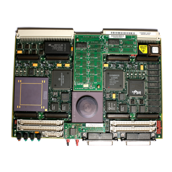
Page 52: Figure 2-1. Mvme162Lx Board Layout
Hardware Preparation and Installation MVME 162-7XX FAIL FUSES SCON ABORT RESET Figure 2-1. MVME162LX Board Layout... -
Page 53: Ip Bus Clock Header (J11)
Hardware Preparation IP Bus Clock Header (J11) J11 selects the speed of the IP bus clock. You can either set the IP bus clock to 8MHz or allow it to match the the local bus clock, which is 32MHz for the MC68040. The factory configuration has a jumper between J11 pins 1 and 2 for an 8MHz clock. -
Page 54: Scsi Terminator Enable Header (J12)
Hardware Preparation and Installation SCSI Terminator Enable Header (J12) The MVME162LX provides terminators for the SCSI bus. The SCSI terminators are enabled/disabled by a jumper on header J12. The SCSI terminators may be configured as follows. Onboard SCSI Bus Terminator Enabled Onboard SCSI Bus Terminator Disabled (Factory Configuration) Note... -
Page 55: Flash Write Protect Header (J16)
Hardware Preparation Removing all jumpers may temporarily disable the SRAM. Do not remove all jumpers from J14, except for storage. Caution Primary Source VMEbus +5V STBY Primary Source Onboard Battery Backup Power Disabled Secondary Source Onboard Battery (For storage only) Secondary Source VMEbus +5V STBY (Factory configuration) Primary Source VMEbus +5V STBY... -
Page 56: Ip Bus Strobe Select Header (J18)
Hardware Preparation and Installation IP Bus Strobe Select Header (J18) Some IP bus implementations make use of the Strobe∗ signal (pin 46) as an input to the IP modules from the IP2 chip. Other IP interfaces require that the strobe be disconnected. With a jumper installed between J18 pins 1 and 2, a programmable frequency source is connected to the Strobe∗... -
Page 57: Eprom/Flash Configuration Header (J20)
Hardware Preparation The following table lists the snoop operations represented by the setting of J19. Table 2-2. J19 Snoop Control Encoding Pins Pins Snoop Operation Snoop disabled Snoop enabled X = don’t care Jumper installed = logic 0 Jumper removed = logic 1 EPROM/Flash Configuration Header (J20) The MVME162LX can be ordered with 2MB of Flash memory and two EPROM sockets ready for the installation of the EPROMs,... -
Page 58: Onboard Flash Disabled
Hardware Preparation and Installation CONFIGURATION 2: 512K x 8 EPROMs CONFIGURATION 1: 256K x 8 EPROMs (FACTORY DEFAULT) CONFIGURATION 3: 1M x 8 EPROMs CONFIGURATION 4: 1M x 8 EPROMs ONBOARD FLASH DISABLED The next four tables show the address range for each EPROM socket in all four configurations. -
Page 59: Table 2-3. Eprom/Flash Mapping - 256K X 8 Eproms
Hardware Preparation Table 2-3. EPROM/Flash Mapping — 256K x 8 EPROMs GPI3 Address Range Device Accessed Removed 1 $FF800000 - $FF83FFFF EPROM A (XU1) $FF840000 - $FF87FFFF EPROM B (XU2) $FFA00000 - $FFBFFFFF Onboard Flash Installed 0 $FF800000 - $FF9FFFFF Onboard Flash $FFA00000 - $FFA3FFFF EPROM A (XU1) $FFA40000 - $FFA7FFFF EPROM B (XU2) -
Page 60: General-Purpose Readable Jumpers Header (J21)
Hardware Preparation and Installation Table 2-6. EPROM/Flash Mapping — 1M x 8 EPROMs, Onboard Flash Disabled GPI3 Address Range Device Accessed Removed 1 $FF800000 - $FF8FFFFF EPROM A (XU1) $FF900000 - $FF9FFFFF EPROM B (XU2) Not used Onboard Flash Installed 0 Not used Onboard Flash $FF800000 - $FF8FFFFF EPROM A (XU1) -
Page 61: Memory Mezzanine Options
Hardware Preparation 162BUG INSTALLED USER CODE INSTALLED GPI7 USER-DEFINABLE USER-DEFINABLE GPI6 USER-DEFINABLE USER-DEFINABLE GPI5 USER-DEFINABLE USER-DEFINABLE GPI4 USER-DEFINABLE USER-DEFINABLE GPI3 IN=FLASH; OUT=EPROM IN=FLASH; OUT=EPROM GPI2 REFER TO 162BUG MANUAL USER-DEFINABLE GPI1 REFER TO 162BUG MANUAL USER-DEFINABLE GPI0 REFER TO 162BUG MANUAL USER-DEFINABLE EPROMs Selected (factory configuration except on no-VMEbus models) Memory Mezzanine Options... -
Page 62: Installation Instructions
Hardware Preparation and Installation When the mezzanines are stacked, the following combinations are possible: Table 2-7. Memory Mezzanine Stacking Options Upper Parity None None Mezzanine DRAM DRAM Parity Lower Mezzanine DRAM DRAM DRAM DRAM Note When equipped with a single memory mezzanine, MVME162LX VMEmodules maintain a single VME slot width. -
Page 63: Ip Installation On The Mvme162Lx
– Connect user-supplied 50-pin cables to J3 and J4 as needed. Because of the varying requirements for each different kind of IP, Motorola does not supply these cables. – Bring the IP cables out the narrow slot in the MVME162LX... -
Page 64: Mvme162Lx Installation
Hardware Preparation and Installation MVME162LX Installation With EPROMs and IPs installed and headers properly configured, proceed as follows to install the MVME162LX in the VME chassis: 1. Turn all equipment power OFF and disconnect the power cable from the AC power source. Inserting or removing modules while power is applied could result in damage to module components. - Page 65 BUS GRANT header for the card slot occupied by the MVME162LX. Note Some VME backplanes (e.g., those used in Motorola ‘‘Modular Chassis’’ systems) have an autojumpering feature for automatic propagation of the IACK and BG signals. Step 6 does not apply to such backplane designs.
-
Page 66: System Considerations
Hardware Preparation and Installation System Considerations The 700/800-series MVME162LX draws power from both the P1 and the P2 connectors on the VMEbus backplane. P2 is also used for the upper 16 bits of data in 32-bit transfers, and for the upper 8 address lines in extended addressing mode. - Page 67 Installation Instructions If you are installing multiple MVME162LXs in an Note MVME945 chassis, do not install one in slot 12. The height of the IP modules may cause clearance difficulties in that slot position. Other MPUs on the VMEbus can interrupt, disable, communicate with, and determine the operational status of the processor(s).
-
Page 68: Figure 2-2. Db-25 Dte-To-Rj-45 Adapter
Hardware Preparation and Installation Figure 2-2 diagrams the pin assignments required in a cable to adapt a DB-25 DTE device to the RJ-45 connectors. DB-25 DTE DEVICE RJ-45 JACK Figure 2-2. DB-25 DTE-to-RJ-45 Adapter Figure 2-3 diagrams the pin assignments required in a cable to adapt a DB-25 DCE device to a RJ-45 connector. -
Page 69: Figure 2-4. Typical Rj-45 Serial Cable
Installation Instructions Figure 2-4 diagrams the pin assignments required in a typical 8- conductor serial cable having RJ-45 connectors at both ends. Note that all wires are crossed. RJ-45 CONNECTOR RJ-45 CONNECTOR Figure 2-4. Typical RJ-45 Serial Cable 2-21... - Page 70 Hardware Preparation and Installation 2-22...
-
Page 71: Overview Of M68000 Firmware
The firmware for the M68000-based (68K) series of board and system level products has a common genealogy, deriving from the debugger firmware currently used on all Motorola M68000-based CPU modules. The M68000 firmware family provides a high degree of functionality and user friendliness, and yet stresses portability and ease of maintenance. - Page 72 162Bug, depending on the outcome of the user program. If you have used one or more of Motorola's other debugging packages, you will find the CISC 162Bug very similar. Some effort has also been made to make the interactive commands more consistent.
-
Page 73: 162Bug Implementation
162Bug Implementation 162Bug Implementation MVME162Bug is written largely in the ‘‘C’’ programming language, providing benefits of portability and maintainability. Where necessary, assembler has been used in the form of separately compiled modules containing only assembler code — no mixed language modules are used. Physically, 162Bug is contained in a single 27C040 DIP EPROM installed in socket XU2, providing 512KB (128K longwords) of storage. - Page 74 Debugger General Information Models with no VMEbus interface have a jumper between pins 7-8 as well. These readable jumpers are read as a register (at $FFF4202D) on the Memory Controller (MC2chip) ASIC. The bit values are read as a zero when the jumper is installed, and as a one when the jumper is removed.
- Page 75 Installation and Startup Note that when the MVME162LX comes up in a cold reset, 162Bug runs in Board Mode. Using the Environment ( ) or commands can make 162Bug run in System Mode. MENU Refer to Appendix A for details. 2.
- Page 76 Debugger General Information After power-up, you can reconfigure the baud rate of the debug port if necessary by using the 162Bug firmware’s Port Format (PF) command. Note In order for high-baud rate serial communication between 162Bug and the terminal to work, the terminal must do some form of handshaking.
-
Page 77: Prom Versions
Autoboot 11. Before using the MVME162LX after the initial installation, set the date and time using the following command line structure: [mmddyyhhmm]|[<+/-CAL>; 162-Bug> For example, the following command line starts the real-time clock and sets the date and time to 10:37 a.m., November 7, 1997: 1107971037 162-Bug>... - Page 78 Debugger General Information controllers and devices in a specified sequence until a valid bootable device containing a boot media is found or the list is exhausted. If a valid bootable device is found, a boot from that device is started. The controller scanning sequence goes from the lowest controller Logical Unit Number (LUN) detected to the highest LUN detected.
-
Page 79: Romboot
As shipped from the factory, 162Bug occupies an EPROM installed in socket XU2. This leaves one socket (XU1) and the Flash memory available for your use. Contact your Motorola sales office for assistance. This function is configured/enabled by the Environment (... -
Page 80: Network Boot
Debugger General Information Network Boot Network Auto Boot is a software routine contained in the 162Bug Flash/PROM that provides a mechanism for booting an operating system using a network (local Ethernet interface) as the boot device. If enabled (via — refer to Appendix A), the Network Auto Boot routine automatically scans for controllers and devices in a specified sequence until a valid bootable device containing a boot media is found or the list is exhausted. -
Page 81: Reset
Restarting the System The debugger has a special feature available for reset conditions. You activate it by pressing the switches at the RESET ABORT same time, releasing first, then releasing seven RESET ABORT seconds later. This ‘‘double-button reset’’ feature instructs the debugger to use the default setup/operation parameters in ROM versus your setup/operation parameters in NVRAM. -
Page 82: Break
Debugger General Information For this reason, abort is most appropriate when terminating a user program that is being debugged. Abort should be used to regain control if the program gets caught in a loop, etc. The target PC, register contents, etc., help to pinpoint the malfunction. Pressing and releasing the switch generates a local board ABORT... -
Page 83: Mpu Clock Speed Calculation
Memory Requirements self test (if system mode) has completed with error MPU clock speed calculation failure After debugger initialization is done and none of the above situations have occurred, the SYSFAIL∗ line is negated. This indicates to the user or VMEbus masters the state of the debugger. In a multi-computer configuration, other VMEbus masters could view the pertinent control and status registers to determine which CPU is asserting SYSFAIL∗. - Page 84 Debugger General Information Type of Memory Present Default Default SRAM DRAM Base Base Address Address A single DRAM mezzanine $00000000 $FFE00000 (onboard SRAM) A single SRAM mezzanine $00000000 A DRAM mezzanine stacked with an SRAM $00000000 $E1000000 mezzanine Two DRAM mezzanines stacked $00000000 $FFE00000 (onboard...
-
Page 85: Disk I/O Support
Disk I/O Support Disk I/O Support 162Bug can initiate disk input/output by communicating with intelligent disk controller modules over the VMEbus. Disk support facilities built into 162Bug consist of command-level disk operations, disk I/O system calls (only via one of the TRAP #15 instructions) for use by user programs, and defined data structures for disk parameters. -
Page 86: Device Probe Function
These following 162Bug commands are provided for disk I/O. Detailed instructions for their use are found in the Debugging Package for Motorola 68K CISC CPUs User's Manual. When a command is issued to a particular controller LUN and device LUN, these LUNs are remembered by 162Bug so that the next disk command defaults to use the same controller and device. -
Page 87: Iot (I/O Teach)
Disk I/O Support IOT (I/O Teach) allows you to change any configurable parameters and attributes of the device. In addition, it allows you to see the controllers available in the system. IOC (I/O Control) allows you to send command packets as defined by the particular controller directly. - Page 88 Refer to the system call descriptions in the Debugging Package for Motorola 68K CISC CPUs User's Manual for details on the format and construction of these standardized user packets. The packets which a controller module expects to be given vary from controller to controller.
-
Page 89: Default 162Bug Controller And Device Parameters
Network I/O Support specifically tailored for the disk drive controller it is sent to. Refer to documentation on the particular controller module for the format of its packets, and for using the command. Default 162Bug Controller and Device Parameters 162Bug initializes the parameter tables for a default configuration of controllers and devices (refer to Appendix B). -
Page 90: Intel 82596 Lan Coprocessor Ethernet Driver
Debugger General Information The booting process is executed in two distinct phases. The first phase allows the diskless remote node to discover its network identify and the name of the file to be booted. The second phase has the diskless remote node reading the boot file across the network into its memory. -
Page 91: Rarp/Arp Protocol Modules
Network I/O Support RARP/ARP Protocol Modules The Reverse Address Resolution Protocol (RARP) basically consists of an identity-less node broadcasting a ‘‘whoami’’ packet onto the Ethernet, and waiting for an answer. The RARP server fills an Ethernet reply packet up with the target's Internet Address and sends it. -
Page 92: Network I/O Error Codes
Debugger General Information Network I/O Error Codes 162Bug returns an error code if an attempted network operation is unsuccessful. Multiprocessor Support The MVME162LX dual-port RAM feature makes the shared RAM available to remote processors as well as to the local processor. This can be done by either of the following two methods. - Page 93 Multiprocessor Support You can only program Flash memory by the MPCR method. Refer to the .PFLASH system call in the Debugging Package for Motorola 68K CISC CPUs User's Manual for a description of the Flash memory program control packet structure.
-
Page 94: Gcsr Method
Debugger General Information In either sequence, an E is placed in the MPCR to indicate that execution is underway just before control is passed to RAM. (Any remote processor could examine the MPCR contents.) If the code being executed in dual-port RAM is to reenter the debug monitor, a TRAP #15 call using function $0063 (SYSCALL .RETURN) returns control to the monitor with a new display prompt. -
Page 95: Diagnostic Facilities
). The diagnostic prompt 162-Diag> appears. Refer to the Debugging Package for Motorola 68K CISC CPUs User's Manual for complete descriptions of the diagnostic routines available and instructions on how to invoke them. Note that some diagnostics depend on restart defaults that are set up only in a particular restart mode. - Page 96 Debugger General Information If either string is in the first location of NVRAM ($FFFC0000), the test process starts. 3-26...
-
Page 97: In This Chapter
4Using the 162Bug Debugger In This Chapter This chapter covers the following subjects: Entering debugger command lines Entering and debugging programs Calling system utilities from user programs Preserving the debugger operating environment Floating point support The 162Bug debugger command set Entering Debugger Command Lines 162Bug is command-driven and performs its various operations in response to user commands entered at the keyboard. - Page 98 Using the 162Bug Debugger The presence of the upward caret ( ) before a character Note indicates that the Control (CTRL) key must be held down while striking the character key. (cancel line) The cursor is backspaced to the beginning of the line. (backspace) The cursor is moved back one position.
-
Page 99: Debugger Command Syntax
Entering Debugger Command Lines Debugger Command Syntax In general, a debugger command is made up of the following parts: The command identifier (i.e., for the Memory Display command). Note that either upper- or lowercase characters are allowed. A port number if the command is set up to work with more than one port. - Page 100 Using the 162Bug Debugger Numeric values may be expressed in either hexadecimal, decimal, octal, or binary notation by immediately preceding them with the proper base identifier. Base Identifier Examples Hexadecimal $FFFFFFFF Decimal & &1974, &10-&4 Octal @456 Binary %1000110 If no base identifier is specified, then the numeric value is assumed to be hexadecimal.
-
Page 101: Address As A Parameter
Entering Debugger Command Lines Valid expression examples: Expression Result (In Hex) Notes FF0011 FF0011 45+99 &45+&99 @35+@67+@10 %10011110+%1001 88<<4 shift left AA&F0 logical AND The total value of the expression must be between 0 and $FFFFFFFF. Address as a Parameter Many commands use addr as a parameter. -
Page 102: Address Formats
Using the 162Bug Debugger Address Formats Table 4-1 summarizes the address formats that are acceptable for address parameters in debugger command lines. Table 4-1. Debugger Address Parameter Formats Format Example Description Absolute address+contents of automatic offset register. N+Rn 130+R5 Absolute address+contents of the specified offset register (not an assembler-accepted syntax). -
Page 103: Offset Registers
Entering Debugger Command Lines In commands with range specified as addr addr, and Note with size option chosen, data at the second (ending) address is acted on only if the second address is a proper boundary for a word or longword, respectively. - Page 104 Using the 162Bug Debugger 0 00000008 5340 SUBQ.W#1,D0 0 0000000A 12D8 LOOP MOVE.B(A0)+,(A1)+ 0 0000000C 51C8FFFC MOVS DBRA D0,LOOP 0 00000010 4CDF0101 MOVEM.L(A7)+,D0/A0 0 00000014 4E75 ****** TOTAL ERRORS 0—— ****** TOTAL WARNINGS 0—— The above program was loaded at address $0001327C. The disassembled code is shown next: 162-Bug>MD 1327C;DI 0001327C 48E78080...
-
Page 105: Port Numbers
Entering and Debugging Programs For additional information about the offset registers, refer to the Debugging Package for Motorola 68K CISC CPUs User's Manual. Port Numbers Some 162Bug commands give you the option to choose the port to be used to input or output. Valid port numbers which may be used for these commands are as follows: 1. -
Page 106: Creating A Program With The Assembler/Disassembler
2. After each source line is entered, it is assembled and the object code is loaded to memory. Refer to the Debugging Package for Motorola 68K CISC CPUs User's Manual for details on the 162Bug Assembler/Disassembler. Downloading an S-Record Object File Another way to enter a program is to download an object file from a host system. -
Page 107: Calling System Utilities From User Programs
You can access various 162Bug routines via one of the MC68040 TRAP instructions, using vector #15. Refer to the Debugging Package for Motorola 68K CISC CPUs User's Manual for details on the various TRAP #15 utilities available and how to invoke them from within a user program. -
Page 108: 162Bug Vector Table And Workspace
Using the 162Bug Debugger 162Bug Vector Table and Workspace As described in the Memory Requirements section of Chapter 3, the 162Bug firmware needs 64KB of read/write memory to operate. 162Bug For ... reserves ... 1024-byte area A user program vector table area 1024-byte area An exception vector table for the debugger itself to use Space for static variables, and initializes these static variables to... -
Page 109: Hardware Functions
Preserving the Debugger Operating Environment Hardware Functions The only hardware resources used by the debugger are the EIA- 232-D ports, which are initialized to interface to the debug terminal and a host. If these ports are reprogrammed, the terminal characteristics must be modified to suit, or the ports should be restored to the debugger-set characteristics prior to reinvoking the debugger. - Page 110 Using the 162Bug Debugger pointer values just before the exception occurred. In this way, the operation of the debugger facility (through an exception) is transparent to users. Example: Trace one instruction using the debugger firmware. 172-Bug> =00010000 =2708=TR:OFF_S._7_N.. =00000000 =0000FFFC =00010000 =1=UD =1=UD...
-
Page 111: Exception Vector Tables
Preserving the Debugger Operating Environment Exception Vector Tables Notice in the preceding example that the value of the target stack pointer register (A7) has not changed even though a trace exception has taken place. Your program may either use the exception vector table provided by 162Bug or it may create a separate exception vector table of its own. -
Page 112: Creating A New Vector Table
Using the 162Bug Debugger Creating a New Vector Table Your program may create a separate vector table in memory to contain its exception vectors. If this is done, the program must change the value of the VBR to point at the new vector table. In order to use the debugger facilities you can copy the proper vectors from the 162Bug vector table into the corresponding vector locations in your program vector table. - Page 113 Preserving the Debugger Operating Environment It may turn out that your program uses one or more of the exception vectors that are required for debugger operation. Debugger facilities may still be used, however, if your exception handler can determine when to handle the exception itself and when to pass the exception to the debugger.
-
Page 114: Floating Point Support
Using the 162Bug Debugger Floating Point Support The floating point unit (FPU) of the MC68040 microprocessor chip is supported in 162Bug. The , and commands have been extended to allow display and modification of floating point data in registers and in memory. Floating point instructions can be assembled and disassembled with the option of the commands. -
Page 115: Single Precision Real
Floating Point Support 4. The sign field, the exponent field, and at least the first digit of the mantissa field must be present (any unspecified digits in the mantissa field are set to zero). 5. Each field must be separated from adjacent fields by an underscore. -
Page 116: Scientific Notation
The commands are explained in CNFG Appendix A. Controllers, devices, and their LUNs are listed in Appendix B or Appendix C. All other command details are explained in the Debugging Package for Motorola 68K CISC CPUs User's Manual. 4-20... -
Page 117: Configure Board Information Block
The 162Bug Debugger Command Set Table 4-3. Debugger Commands Command Title Command Line Syntax Mnemonic Automatic Bootstrap AB [;V] Operating System NOAB No Autoboot NOAB One Line Assembler AS addr Block of Memory Compare BC range addr [; B|W|L] Block of Memory Fill BF range data [increment] [;... - Page 118 Using the 162Bug Debugger Table 4-3. Debugger Commands (Continued) Command Title Command Line Syntax Mnemonic ECHO Echo String ECHO [port] {hexadecimal number} {'string'} Set Environment to ENV [; [D]] Bug/Operating System Go Direct (Ignore GD [addr] Breakpoints) Go to Next Instruction Go Execute User Program GO [addr] Go to Temporary Breakpoint...
- Page 119 The 162Bug Debugger Command Set Table 4-3. Debugger Commands (Continued) Command Title Command Line Syntax Mnemonic MENU Menu MENU Memory Modify MM addr [; [[B|W|L|S|D] [A] [N]]|[DI]] Memory Map Diagnostic MMD range increment [; B|W|L] Memory Set MS addr {hexadecimal number} {'string'} Memory Write MW addr data [;...
- Page 120 Using the 162Bug Debugger Table 4-3. Debugger Commands (Continued) Command Title Command Line Syntax Mnemonic ROMboot Enable RB [; V] NORB ROMboot Disable NORB Register Display RD {[+|-|=] [dname] [/]} {[+|-|=] [reg1[-reg2]] [/]} [; E] REMOTE Connect the Remote Modem REMOTE to CSO RESET...
- Page 121 This command is used to display and configure the board information block. This block is resident within the Non-Volatile RAM (NVRAM). Refer to the Debugging Package for Motorola 68K CISC CPUs User's Manual for the actual location. The information block contains various elements detailing specific operation parameters of the hardware.
- Page 122 Configure and Environment Commands Parity Memory Mezzanine (PWA) Serial Number = " " Static Memory Mezzanine Artwork (PWA) Identifier = " " Static Memory Mezzanine (PWA) Serial Number = " " ECC Memory Mezzanine #1 Artwork (PWA) Identifier = " "...
-
Page 123: Set Environment To Bug/Operating System
Set Environment to Bug/Operating System Modification is possible through use of the command’s option. At the end of the modification session, you are prompted for the update to Non-Volatile RAM (NVRAM). A response must be made for the update to occur; any other response terminates the update (disregards all changes). -
Page 124: Table A-1. Env Command Parameters
Configure and Environment Commands If the command is invoked with no options on the command line, you are prompted to configure all operational parameters. If command is invoked with the option , ROM defaults will be loaded into NVRAM. The parameters to be configured are listed in the following table. Table A-1. - Page 125 Set Environment to Bug/Operating System Table A-1. ENV Command Parameters (Continued) ENV Parameter and Options Default Meaning of Default Auto Boot at power-up only Auto Boot is attempted at power-up reset [Y/N] only. Auto Boot Controller LUN LUN of a disk/tape controller module currently supported by the Bug.
- Page 126 Configure and Environment Commands Table A-1. ENV Command Parameters (Continued) ENV Parameter and Options Default Meaning of Default Network Auto Boot Enable Network Auto Boot function is disabled. [Y/N] Network Auto Boot at power- Network Auto Boot is attempted at up only [Y/N] power up reset only.
- Page 127 Set Environment to Bug/Operating System Table A-1. ENV Command Parameters (Continued) ENV Parameter and Options Default Meaning of Default Memory Search Ending 00100000 Top limit of the Bug's search for a work Address page. If a contiguous block of memory, 64KB in size, is not found in the range specified by Memory Search Starting Address and Memory Search Ending...
- Page 128 Configure and Environment Commands Table A-1. ENV Command Parameters (Continued) ENV Parameter and Options Default Meaning of Default Memory Search Delay FFFFD20F Default address is $FFFFD20F. This is the Address MVME162LX GCSR (global control/status register) GPCSR0 as accessed through VMEbus A16 space. It is assumed that the MVME162LX GRPAD (group address) and BDAD (board address within group) switches are set to...
- Page 129 Set Environment to Bug/Operating System Table A-1. ENV Command Parameters (Continued) ENV Parameter and Options Default Meaning of Default Memory Configuration Defaults: The default configuration for Dynamic RAM mezzanine boards will position the mezzanine with the largest memory size to start at the address selected with the ENV parameter ‘‘Base Address of Dynamic Memory’’.
- Page 130 Configure and Environment Commands Table A-1. ENV Command Parameters (Continued) ENV Parameter and Options Default Meaning of Default ENV asks the following series of questions to set up the VMEbus interface for the MVME162LX modules. You should have a working knowledge of the VMEchip2 as given in the MVME162LX Embedded Controller Programmer's Reference Guide in order to perform this configuration.
- Page 131 Set Environment to Bug/Operating System Table A-1. ENV Command Parameters (Continued) ENV Parameter and Options Default Meaning of Default Slave Ending Address #2 00000000 Ending address of the local resource that is accessible by the VMEbus. Default is 0. Slave Address Translation 00000000 Works the same as Slave Address Address #2...
- Page 132 Configure and Environment Commands Table A-1. ENV Command Parameters (Continued) ENV Parameter and Options Default Meaning of Default Master Control #2 Defines the access characteristics for the address space defined with this master address decoder. Default is $00. Master Enable #3 [Y/N] Yes, set up and enable the Master Address (Depends Decoder #3.
- Page 133 Set Environment to Bug/Operating System Table A-1. ENV Command Parameters (Continued) ENV Parameter and Options Default Meaning of Default Master Address Translation 00000000 Allows the VMEbus address and the local Address #4 address to differ. The value in this register is the base address of the VMEbus resource that is associated with the starting and ending address selection...
-
Page 134: Configuring The Industrypacks
Configure and Environment Commands Table A-1. ENV Command Parameters (Continued) ENV Parameter and Options Default Meaning of Default VMEC2 GCSR Group Base Specifies the group address ($FFFFXX00) Address in Short I/O for this board. Default = $D2. VMEC2 GCSR Board Base Specifies the base address ($FFFFD2XX) Address in Short I/O for this board. - Page 135 Set Environment to Bug/Operating System Base address for mapping IP modules. Only the upper 16 bits are significant. IP D/C/B/A Memory Size = 00000000? Define the memory size requirements for the IP modules: Bits Register Address 31-24 FFFBC00F 23-16 FFFBC00E 15-08 FFFBC00D 07-00...
- Page 136 Configure and Environment Commands IP D/C/B/A Interrupt 0 Control = 00000000? Define the interrupt control requirements for the IP modules channel 0: Bits Register Address 31-24 FFFBC016 23-16 FFFBC014 15-08 FFFBC012 07-00 FFFBC010 IP D/C/B/A Interrupt 1 Control = 00000000? Define the interrupt control requirements for the IP modules channel 1: Bits...
- Page 137 Set Environment to Bug/Operating System ENV warning example: WARNING: Memory MAP Overlap Condition Exists S-Address E-Address Enable Overlap M-Type Memory-MAP-Name $00000000 $FFFFFFFF Yes Master Local Memory (Dynamic RAM) $FFE00000 $FFE7FFFF Yes Master Static RAM $01000000 $EFFFFFFF Yes Master VMEbus Master #1 $00000000 $00000000 No Master...
- Page 138 Configure and Environment Commands A-18...
-
Page 139: Disk/Tape Controller Modules Supported
BDisk/Tape Controller Data Disk/Tape Controller Modules Supported The following VMEbus disk/tape controller modules are supported by the 162Bug. The default address for each controller type is First Address and the controller can be addressed by First CLUN during commands BH, BO, or IOP, or during TRAP #15 calls .DSKRD or .DSKWR. -
Page 140: Disk/Tape Controller Default Configurations
Disk/Tape Controller Data Disk/Tape Controller Default Configurations Note SCSI Common Command Set (CCS) devices are the only ones tested by Motorola Computer Group. CISC Embedded Controllers -- 7 Devices Controller LUN Address Device LUN Device Type $XXXXXXXX SCSI Common Command Set... - Page 141 Disk/Tape Controller Default Configurations MVME328 -- 14 Devices Controller LUN Address Device LUN Device Type $FFFF9000 SCSI Common Command Set (CCS), which may be any of these: - Removable flexible direct access $FFFF9800 (TEAC style) - CD-ROM $FFFF4800 - Sequential access $FFFF5800 Same as above, but these are only available if the daughter card for the...
- Page 142 Disk/Tape Controller Data IOT Command Parameters for Supported Floppy Types The following table lists the proper IOT command parameters for floppies used with boards such as the MVME328 and MVME162LX. Floppy Types and Formats IOT Parameter DSDD5 PCXT8 PCXT9 PCXT9_3 PCAT Sector Size 0- 128 1- 256 2- 512...
-
Page 143: Iot Command Parameters For Supported Floppy Types
IOT Command Parameters for Supported Floppy Types Floppy Types and Formats IOT Parameter DSDD5 PCXT8 PCXT9 PCXT9_3 PCAT Number of Logical Blocks 09F8 0500 05A0 0B40 12C0 1680 2D00 (100 in size) Number of Bytes in Decimal 653312 327680 368460 737280 1228800 1474560 2949120 Media Size/Density... - Page 144 Disk/Tape Controller Data...
-
Page 145: Network Controller Modules Supported
CNetwork Controller Data Network Controller Modules Supported The following VMEbus network controller modules are supported by the MVME162BUG firmware. The default address for each type and position is showed to indicate where the controller must reside to be supported by MVME162BUG. The controllers are accessed via the specified CLUN and DLUNs listed here. - Page 146 Network Controller Data...
-
Page 147: Solving Startup Problems
DTroubleshooting CPU Boards Solving Startup Problems In the event of difficulty with your CPU board, try the simple troubleshooting steps on the following pages before calling for help or sending the board back for repair. Some of the procedures will return the board to the factory debugger environment. - Page 148 Troubleshooting CPU Boards Table D-1. Troubleshooting MVME162LX Boards (Continued) Condition Possible Problem Try This: II. There is a A. The keyboard or Recheck the keyboard and/or mouse connections and display on the mouse may be power. terminal, but connected input from the incorrectly.
- Page 149 Solving Startup Problems Table D-1. Troubleshooting MVME162LX Boards (Continued) Condition Possible Problem Try This: IV. Continued 2. At the command line prompt, type in: env;d <CR> This sets up the default parameters for the debugger environment. 3. When prompted to Update Non-Volatile RAM, type in: y <CR>...
- Page 150 Troubleshooting CPU Boards Table D-1. Troubleshooting MVME162LX Boards (Continued) Condition Possible Problem Try This: V. The debugger is A. No apparent No further troubleshooting steps are required. in system mode problems — and the board troubleshooting autoboots, or is done. the board has passed selftests.
- Page 151 Index Numerics 162Bug (MVME162Bug) firmware 2-3, 3-1, 4-1 backplane jumpers 2-17 command set 4-20 Backus-Naur syntax, debugger commands default controller and device and 4-3 parameters 3-19 base address, DRAM 2-18 implementation 3-3 base and top addresses 4-7 installation 3-3 base identifier, numeric values and 4-4 stack space 3-14 battery 1-18 static variable space 3-14...
- Page 152 DLUN (device LUN) B-2, C-1 MVME162LX board 2-1 documentation VMEbus interface A-10 non-Motorola single publications 1-5 connections, serial cable 2-20 other applicable Motorola publications 1-4 connectors on J17 (serial) 4-9 double precision real (floating point connectors, MVME162LX 1-27 format) 4-19 console port 4-9...
- Page 153 Index IndustryPack (IP) modules 1-22 configuring A-14 false, definition of 1-12 defining general control requirements A-15 FCC compliance 1-11 defining interrupt control requirements A-16 features, MVME162LX 1-6 defining memory size requirements A-15 firmware 2-3 input/output control, terminal 4-1 console 3-5 installation implementation 3-3 considerations 2-18...
- Page 154 MPU clock speed calculation 3-13 prompt, debugger 4-1 multiprocessor support 3-22 protocol modules MVME162Bug (162Bug) 1-16, 2-3, 3-1 BOOTP 3-21 MVME162LX RARP/ARP 3-21 block diagram 1-14 TFTP 3-21 features 1-6 UDP/IP 3-20 installation 2-16 pseudo-registers 4-7 specifications 1-8 publications, non-Motorola 1-5 IN-4...
- Page 155 Index status bit, definition of 1-12 string literals, numeric values and 4-4 range (command syntax) 4-3 switches 1-13 RARP/ARP protocol modules 3-21 switching directories 3-25 reading a program from disk 4-10 syntactic variables, command lines and 4-3 registers, offset 4-7 system calls, 162Bug 3-17 related documentation 1-2 system console 3-5...
- Page 156 Index watchdog timer 1-24 Z85230 serial communications controllers (SCCs) 3-6 IN-6...