
Related Manuals for Panasonic TY-FB11DHD


Summary of Contents for Panasonic TY-FB11DHD
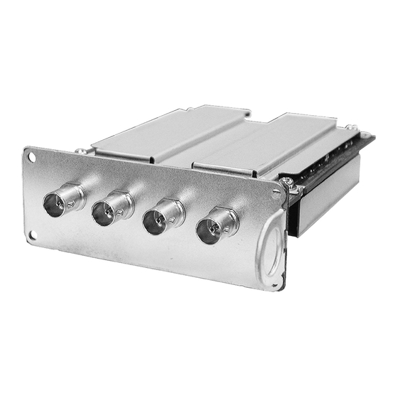
- Page 1 ORDER NO.ITD0810106CE B34 Canada: D10 Dual Link HD-SDI Terminal Board TY-FB11DHD Model No. © Panasonic Corporation 2008. Unauthorized copying and distribution is a violation of law.
-
Page 2: Safety Precautions
1 Safety Precautions 1.1. General Guidelines 1. When conducting repairs and servicing, do not attempt to modify the equipment, its parts or its materials. 2. When wiring units (with cables, flexible cables or lead wires) are supplied as repair parts and only one wire or some of the wires have been broken or disconnected, do not attempt to repair or re-wire the units. -
Page 3: Prevention Of Electrostatic Discharge (Esd) To Electrostatically Sensitive (Es) Devices
2 Warning 2.1. Prevention of Electrostatic Discharge (ESD) to Electrostatically Sensitive (ES) Devices Some semiconductor (solid state) devices can be damaged easily by static electricity. Such components commonly are called Elec- trostatically Sensitive (ES) Devices. Examples of typical ES devices are integrated circuits and some field-effect transistors and semiconductor [chip] components. -
Page 4: About Lead Free Solder (Pbf)
2.2. About lead free solder (PbF) Note: Lead is listed as (Pb) in the periodic table of elements. In the information below, Pb will refer to Lead solder, and PbF will refer to Lead Free Solder. The Lead Free Solder used in our manufacturing process and discussed below is (Sn+Ag+Cu). That is Tin (Sn), Silver (Ag) and Copper (Cu) although other types are available. -
Page 5: Installation Instructions
3 Installation Instructions... - Page 6 4 Operating Instructions...
- Page 11 5 Disassembly and Assembly Instructions 5.1. Remove the HSC Board 1. Remove the screws ( ×4 ) and then remove the HSC terminal fixed metal. 2. Remove the screws( ×4 ) and then remove the Shield case A/B and HSC Board.
-
Page 13: Block Diagram
AUDIO DAC AOUT AIN+ Q3602 TP3501 TP3701 BIN+ Q3604 SCLK_TCK SCLK_TCK BOUT SDIN_TDI SDIN_TDI SDOUT_TDO SDOUT_TDO Q3605 Q3601 CS_L_TMS CS_L_TMS Q3603 IC3310 STBY+5V EEPROM IIC SCL IC3408 IIC DAT LEVEL SHIFT FACTORY TY-FB11DHD TY-FB11DHD HSC-Board Block Diagram HSC-Board Block Diagram... - Page 14 7 Schematic Diagram 7.1. Schematic Diagram Note...
- Page 15 0.1u 0.1u NO USE CANC IC3704 SYNC YANC IC3704 R3763 LINKB_H R3781 R3780 R3779 IC3704 R3762 LINKB_V IC3704 R3782 R3761 LINKB_F IC3704 R3783 R3792 FIFO_LD_B FIFO_LD_L IC3704 SDO_ENA SDO_EN/DIS_L IC3704 TY-FB11DHD TY-FB11DHD HSC-Board (1/4) Schematic Diagram HSC-Board (1/4) Schematic Diagram...
- Page 16 C3354 0.1u DOUT0 IC3304 0.1u NON USE SYNC R3363 LINKA_H CANC IC3304 IC3304 R3362 LINKA_V YANC IC3304 IC3304 R3361 LINKA_F IC3304 R3392 FIFO_LD_A R3382 FIFO_LD_L IC3304 SDO_ENA SDO_EN/DIS_L IC3304 R3383 TY-FB11DHD TY-FB11DHD HSC-Board (2/4) Schematic Diagram HSC-Board (2/4) Schematic Diagram...
- Page 17 IC3403 IO_L13P_1/A2 IC3403 ODD3_OUT1 ODD2_OUT2 R3518 ODD1_OUT1 IO_L01N_0 IC3403 IO_L06P_1 IC3403 IO_L18N_1/LDC0 IC3403 ODD3_OUT0 ODD2_OUT1 R3519 ODD1_OUT0 IO_L01P_0 IC3403 IO_L06N_1 IC3403 IO_L17P_1 IC3403 ODD2_OUT0 R3407 IO_L04N_1/VREF_1 IC3403 EXB28V820JX R3405 EXB28V820JX TY-FB11DHD TY-FB11DHD HSC-Board (3/4) Schematic Diagram HSC-Board (3/4) Schematic Diagram...
- Page 18 MODE SLOT_SRQ R3514 IO_L11P_0/GCLK10 IC3403 Dual-in/Dual-out R3492 R3497 Single-in/Single-out R3535 IC3310 IO_L08N_0/GCLK5 IC3403 Single-in/Dual-out TVRQ311 Trigger Edge Select Clock Rise Edge EEPROM SLOT_SCL Clock Fall Edge SLOT_SDA HSC-BOARD TXNHSC101FA (4/4) TY-FB11DHD TY-FB11DHD HSC-Board (4/4) Schematic Diagram HSC-Board (4/4) Schematic Diagram...
-
Page 19: Printed Circuit Board
B 4 0 I C 4 1 0 B 3 9 C 5 0 5 Q 6 0 5 P A 8 0 1 A 4 0 A 3 9 T P 8 0 2 TY-FB11DHD TY-FB11DHD HSC-BOARD TXNHSC101FA HSC-BOARD TXNHSC101FA... -
Page 21: Exploded View And Replacement Parts List
9 Exploded View and Replacement Parts List 9.1. Exploded View and Mechanical Replacement Parts List 9.1.1. Exploded View... - Page 22 9.1.2. Mechanical Replacement Parts List Ref. Safety Part No. Part Name & Description Q'ty Remarks TPCC52601A CARTON BOX TPDF1103 CUSHION TPEH135 PROTECT COVER TBMU920 TERMINAL SHEET TQZH461-2 INSTRUCTION SHEET (SLOT CHANGE) TQZJ026-1 INSTRUCTION SHEET XZBT6506 POLY BAG THEL0239 SCREW TQE6691 POLY BAG THEL027N SCREW...
-
Page 23: Electrical Replacement Parts List
9.2. Electrical Replacement Parts List 9.2.1. Replacement Parts List Notes... - Page 24 9.2.2. Electrical Replacement Parts List Safety Ref. No. Part No. Part Name & Pcs Remarks Description Safety Ref. No. Part No. Part Name & Pcs Remarks C3513 F2G1C470A022 E 47UF, 16V Description C3514 F1G1C104A077 C 0.10UF, K, 16V C3515,16 F1J0J1060004 C 0.010UF, K, C3301,02 ECJ1VB0J105K C 1UF, K, 6.3V C3305...
- Page 25 Safety Ref. No. Part No. Part Name & Pcs Remarks Safety Ref. No. Part No. Part Name & Pcs Remarks Description Description C3730-37 F1G1C104A077 C 0.10UF, K, 16V Q3602 2SD0601ARL TRANSISTOR C3738,39 F1J0J1060004 C 0.010UF, K, Q3603 2SD1979STX TRANSISTOR Q3604 2SD0601ARL TRANSISTOR C3747...
- Page 26 Safety Ref. No. Part No. Part Name & Pcs Remarks Safety Ref. No. Part No. Part Name & Pcs Remarks Description Description R3460-65 D0GB103JA057 M 10K OHM J 1/ R3641 ERJ3GEYJ101 M 100 OHM,J,1/ R3472 ERJ3GEYJ220 M 22 OHM,J,1/16W R3642 ERJ3GEYJ104 M 100KOHM,J,1/ R3473...