
Related Manuals for LG DP9821P


Summary of Contents for LG DP9821P
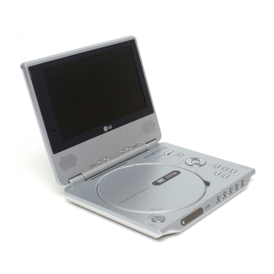
- Page 1 All manuals and user guides at all-guides.com PORTABLE DVD SERVICE MANUAL MODEL : DP9821P(DP9821BPM) CAUTION BEFORE SERVICING THE UNIT, READ THE “SAFETY PRECAUTIONS” IN THIS MANUAL. JUNE, 2005 P/NO : 3829RHP047H Printed in Korea...
- Page 2 All manuals and user guides at all-guides.com CONTENTS SECTION 1 ..SUMMARY SECTION 2 ..EXPLODED VIEWS SECTION 3 ..ELECTRICAL SECTION 4 ..REPLACEMENT PARTS LIST...
- Page 3 All manuals and user guides at all-guides.com SECTION 1 SUMMARY CONTENTS PRODUCT SAFETY SERVICING GUIDELINES FOR VIDEO PRODUCTS ..... 1-3 SERVICING PRECAUTIONS ....................1-4 SPECIFICATIONS ........................1-5...
- Page 4 All manuals and user guides at all-guides.com PRODUCT SAFETY SERVICING GUIDELINES FOR VIDEO PRODUCTS CAUTION : DO NOT ATTEMPT TO MODIFY THIS PRODUCT IN ANY WAY, SUBJECT : X-RADIATION NEVER PERFORM CUSTOMIZED INSTALLATIONS WITHOUT MANUFAC- 1. BE SURE PROCEDURES AND INSTRUCTIONS TO ALL SERVICE PER- TURER’S APPROVAL.
- Page 5 All manuals and user guides at all-guides.com SERVICING PRECAUTIONS CAUTION : Before servicing the PORTABLE DVD covered Electrostatically Sensitive (ES) Devices by this service data and its supplements and addends, read Some semiconductor (solid state) devices can be damaged and follow the SAFETY PRECAUTIONS. NOTE : if unfore- easily by static electricity.
-
Page 6: Specifications
All manuals and user guides at all-guides.com SPECIFICATIONS [DVD player] Power supply DC 9.5 V (AC adapter terminal), DC 7.4 V (Battery) Power consumption 15 W with battery Weight 1.46 lbs (0.66 kg) (without battery pack) External dimensions (W X D X H) 7.5 x 1.1 x 6.3 inches (190 x 28 x 159.5 mm) Signal system Laser... - Page 7 All manuals and user guides at all-guides.com SECTION 2 EXPLODED VIEWS CONTENTS EXPLODED VIEWS ........................2-2 • Cabinet and Main Frame Section ....................2-2 • Packing Accessory Section .....................2-4...
-
Page 8: Exploded Views
All manuals and user guides at all-guides.com EXPLODED VIEWS • Cabinet and Main Frame Section... -
Page 9: Packing Accessory Section
All manuals and user guides at all-guides.com • Packing Accessory Section 831 ADAPTER DC DC 12 BATTERY 830 AC ADAPTER REMOCON 814 PLUG ASS'Y OWNER'S MANUAL R/C BATTERY 804A R/C BATTERY BAG 802A ACCESSORY BOX PACKING 802B GIFT BOX OPTIONAL PARTS... -
Page 10: Table Of Contents
All manuals and user guides at all-guides.com SECTION 3 ELECTRICAL CONTENTS LCD PART ........................3-2 ELECTRICAL TROUBLE SHOOTING GUIDE ............3-11 DETAILS AND WAVEFORMS ON SYSTEM TEST AND DEBUGGING....3-20 BLCOK DIAGRAMS ....................3-29 CIRCUIT DIAGRAM ....................3-31 PRINTED CIRCUIT DIAGRAMS ................3-49... -
Page 11: Lcd Part
All manuals and user guides at all-guides.com LCD PART 1) Power measuring Measure each power after power supply. C83(-) : -14.5V, C82(+) : +15V, C100 : +7.5V, C97(+) : +5V, C43(+) : 3.3V 2) VCOM waveform adjustment Adjust the VCOM level while changing the VR1 as below waveform by using the scope in the C84. - Page 12 All manuals and user guides at all-guides.com LCD TROUBLE SHOOTING GUIDE(1/2) Appear shadow form interference in black background DESPLAY CONDITION? INVERTOR ABNORMAL There is only bring light.(LCD B/D abnormal) FUSE NORMAL? Fuse Replace IC(U1) NORMAL OPERAE IC(U1) Check and Replace D2, D3, D8 Check 7.5V, 15V, -14.5V Normal? Main B/D on located...
- Page 13 All manuals and user guides at all-guides.com LCD TROUBLE SHOOTING GUIDE(2/2) LCD MODE CONT SIGNAL? MAIN B/D Check ALL “LOW”(MORMAL CONDITION)? TFT LCD PRESSURE VOLTAGE? Power source and D2,D3,U4 Check +15V,- 14.5V,+5V Replace TFT LCD NORMAL? Readjust as adjustement standard COLOR ADJUSTING NORMAL? EACH CONNECTOR? Replace and Reassemble...
- Page 14 All manuals and user guides at all-guides.com LCD BLOCK DIAGRAM TERAMINS T100 LCD 7î WIDE VCOM -14.5V 7.5V INVERTER DC-DC CONV CVBS...
- Page 15 All manuals and user guides at all-guides.com LCD CIRCUIT DIAGRAMS VDD22 AVDD33 VDD33 VDD22 0.1uF 0.1uF 100uF/6.3V AC0/ACB0 AC1/ACB1 AC2/ACB2 VDT0 0.1uF CVBS0/AY0 VDT1 CVBS1/AY1 VDT2 CVBS2/AY2 VDT3 VDT4 CVBS3/ACR0 VDT5 0.1uF CVBS4/ACR1 VDT6 1RP1 CVBS5/ACR2 VDT7 CBMID TERAWINS T100 CBMID VCLK CGMID...
- Page 16 All manuals and user guides at all-guides.com L13 10uH 4.7uF/25V -15V SPR+ VDD33 SPR- 0.1uF VCOM SPL+ SPL- STH1 CPH3 CPH2 GND1 CPH1 10uH IRON(1206) RESET_T REST 10u/16V STH2 FB 10R GNDD GND2 +15V GND3 10uH IRON(1206) VGOFF GND4 100n CVBS CVBS_IN 10u/25V...
- Page 17 All manuals and user guides at all-guides.com +7.5V BIAS 0.1uF 0.1uF 0.1uF 0.1uF R3 20K 0.1uF 0.1uF 0.1uF 100uF/6.3V AVDD33 47uF/16V 0.1uF 0.1uF 0.1uF 0.1uF 0.1uF 0.1uF 0.1uF 0.1uF 100uF/6.3V 0.1uF VDD33 0.1uF 0.1uF 0.1uF 0.1uF 0.1uF 0.1uF 100uF/6.3V 10uH VDD33 VDD33 +3.3V...
- Page 18 All manuals and user guides at all-guides.com 2.7uH SPL+ AVDD33 SPL- 0603 680pF 330pF 0.1uF COMP SPR+ SPR- RSET 2.7uH R5 0 0603 680pF 330pF CM1117SCM223 2.5V PCBCOMPONENT_1 +2.5V VDD33 2.7uH R7 0 CVBS 0603 47uF/6.3V 680pF 330pF...
- Page 19 All manuals and user guides at all-guides.com LCD P.C. BOARD ( TOP VIEW ) ( BOTTOM VIEW ) 3-10...
-
Page 20: Electrical Trouble Shooting Guide
All manuals and user guides at all-guides.com ELECTRICAL TROUBLE SHOOTING GUIDE 1. Power (DC-DC Converter) Circuit NO POWER ON NO POWER ON by ADAPTOR by BATTERY Is ADAPTOR Replace Is BATTERY OK? Replace BATTERY OUT 9.5V. ADAPTOR Is F101 OK. Replace F101 Is D106 OK? Replace D 106... - Page 21 All manuals and user guides at all-guides.com NO LCD NO +1.8V NO +3.3V NO +5V NO -5V POWER Replace Replace Is IC(U105) IC(U102). IC(U101) A+5V OK? Is IC(U106) Replace Is IC(U101) pin6 3.3v OK? IC(U106). +5v OK? Is C102 3.3V Replace Replace Replac F102...
- Page 22 All manuals and user guides at all-guides.com B. AUDIO OUT ABNORMAL C.VIDEO OUT ABNORMAL AUDIO OUT VIDEO OUT ABNORMAL ABNORMAL Check Audio Jack & Check Video Jack & Mode Mode Check Video signals Check +5V, -5V from MPEG Check Signals from Check IC(U401) MPEG Replace IC(U301)
- Page 23 All manuals and user guides at all-guides.com G.VIDEO OUT ABNORMAL F. PICTURE ABNORMAL PICTURE ABNORMAL DISC ERROR Check the disc. Check Disc YES(If OK) Refer to Servo part Refer to Servo part If OK YES(If OK) Check MPEG_CLK Replace B/D Signal of MPEG part YES(If OK) Check MPEG...
- Page 24 All manuals and user guides at all-guides.com 2. MPEG Circuit Power is on Does Logo appear Check power & clock. on the screen? Does the Check CD/DVD DSP output moving picture of the DVD Disc Is MPEG data signal normal? play on the screen signal.
- Page 25 All manuals and user guides at all-guides.com 3. RF/SERVO CIRCUIT Laser off Put disc in? Check the related circuit Proper RFL signal Disc ID is correct? on MT1389 RFL signal . on MT1389? Check the RFL connection between CON200 and MT1389. Proper Check DMSO related DMSO signal on...
- Page 26 All manuals and user guides at all-guides.com Proper Check connections between signals on A, B, C, Focus ON OK? MT1389 and pick-up head. D of MT1389 Check the related circuit Proper FEO signal on MT1389 FEO sugnal . on MT1389? Check IC500 IC Check the related Proper FEO signal...
- Page 27 All manuals and user guides at all-guides.com Audio Normal DAC received Check connection between MT1389 Audio output & Audio DAC. (Check VRST#, ACLK, correct data stream? when disc playback? ABCK, ASDAT3) Normal Check the related circuit of Audio DAC Audio DAC. (Check Audio out? (IC702) out Pin 14, 15,18,19) Check Audio filter, amplify,...
- Page 28 All manuals and user guides at all-guides.com 4. Chargeing Circuit No turn on Red LED Is 8.4V of J601_Pin1 OK? Is Q707 OK? Replace Q707. Is IC(U703)OK? Replace IC(U703). Is L701,C706,C709 Replace L701, C706, C709. Is IC(U701) OK? Replace IC(U701). Is IC702 OK? Replce IC702.
-
Page 29: Details And Waveforms On System Test And Debugging
All manuals and user guides at all-guides.com DETAILS AND WAVEFORMS ON SYSTEM TEST AND DEBUGGING 1. SYSTEM 27MHz CLOCK,RESET,FLASH R/W SIGNAL 1) MT1389 main clock is at 27MHz(X500) 3.8V, 27MHz FIG 1-1 2. SDRAM CLOCK 1) MT1389 main clock is at 27MHz(X501) DCLK = 93MHz, Vp-p=2.2, Vmax=2.7V (IC500 PIN 229, 228) FIG 2-1... - Page 30 All manuals and user guides at all-guides.com 3. DISC TYPE JUDGEMENT WAVEFORM F+(IC200 PIN 24) FE(IC500 PIN 31) RFL(IC500 PIN 6) FIG 7-1 (DVD) F+(IC200 PIN 24) FE(IC500 PIN 31) RFL(IC500 PIN 6) FIG 7-2 (DVD) 3-21...
- Page 31 All manuals and user guides at all-guides.com F+(IC200 PIN 24) FE(IC500 PIN 31) RFL(IC500 PIN 6) FIG 7-3 (CD) F+(IC200 PIN 24) FE(IC500 PIN 31) RFL(IC500 PIN 6) FIG 7-4 (CD) 3-22...
- Page 32 All manuals and user guides at all-guides.com 4. FOCUS ON WAVEFORM FE(IC500 PIN 31) FOSO(IC200 PIN9) F+(IC200 PIN 24) F-(IC200 PIN 23) FIG 8-1 (DVD) FE(IC500 PIN 31) FOSO(IC200 PIN9) F+(IC200 PIN 24) F-(IC200 PIN 23) FIG 8-2 (CD) 3-23...
- Page 33 All manuals and user guides at all-guides.com 5. SPINDLE CONTROL WAVEFORM (NO DISC CONDITION) DMSO(1.4V/1.8V) (IC501 PIN 18) SP-(3.6V/2.4V) (IC202 PIN 10) SP+(3.6V/4.8V) (IC202 PIN 11) FIG 9-1 6. TRACKING CONTROL RELATED SIGNAL(System checking) TE(IC500 PIN 32) TRSO(IC200 PIN 8) T-(IC200 PIN 20) T+(IC200 PIN 19) FIG 10-1(DVD)
- Page 34 All manuals and user guides at all-guides.com TE(IC500 PIN 32) TRSO(IC200 PIN 8) T-(IC200 PIN 20) T+(IC200 PIN 19) FIG 10-2(CD) 7. RF WAVEFORM RFOP(2.3V/1.1V) (IC500 PIN 25) RFON(0.8V/2.0V) (IC500 PIN 26) FIG 11-1 3-25...
- Page 35 All manuals and user guides at all-guides.com 8. MT1389 AUDIO OPTICAL AND COAXIAL OUTPUT (ASPDIF) (IC500 PIN 225) FIG 12-1 9. MT1389 VIDEO OUTPUT WAVEFORM 1) Full colorbar signal(CVBS) (IC604 PIN 23) FIG 13-1 3-26...
- Page 36 All manuals and user guides at all-guides.com 2) Y (IC604 PIN 21) FIG 13-2 3) C (IC604 PIN 26) FIG 13-3 3-27...
- Page 37 All manuals and user guides at all-guides.com 10. AUDIO OUTPUT FROM AUDIO DAC 1) Audio L/R (JK601 PIN 4,5) FIG 14-1 2) Audio related Signal ASDAT 0 ASDAT0(IC301 PIN 3) ABCK(IC301 PIN 4) ALRCK(IC5301 PIN 5) FIG 14-2 3-28...
- Page 38 All manuals and user guides at all-guides.com BLOCK DIAGRAMS 1. OVERALL BLOCK DIAGRAM A,B,C,D,RFIP,TNI,TPI MDI1,SUBA,SUBB LD01,LD02,IOA,V20 V,HV+/-,W,HW+/- U,HU+/- FO+,FO-,TR+,TR- STEP1+/-,STEP2+/- DECK MECHANISM 3-29...
- Page 39 All manuals and user guides at all-guides.com 2. POWER(DC-DC CONVERTER)BLOCK DIAGRAM DCPWR E+5V S+5V A+5V A-5V D+3.3V A+3.3V D+1.8V +15V -14.5V 7.5V U104 BD6111FV U105 RT9701 AAT1102 U101 U102 MP1410 MP1410 Q107 U701 U702 SI4435D Y SI4435D Y GT6312 CH_EN PWRCTL_ 3.3V PWRCTL_5V From...
-
Page 40: Circuit Diagram
All manuals and user guides at all-guides.com CIRCUIT DIAGRAMS 1. MAIN POWER CIRCUIT DIAGRAM POWER INPUT DC+9.8V GT119 TP101 TP106 J101 F101 PWR_SRC D103 C130 UDZS16B 0.1U D105 C129 C142 0.1U RB081L-20 D106 HEC3110 220uF/16V D104 RB081L-20 R117 UDZS16B POWERJACK GT120 TP108 TP109... - Page 41 All manuals and user guides at all-guides.com 2. SERVO CIRCUIT DIAGRAM R206 R208 100K A+5V Q202 R209 The countermeasure of static electricity 2N3904 D202 STZ6.8N(OPEN) R207 100K D203 CON200 Q200 Q201 STZ6.8N(OPEN) 2SK3018 2SK3018 LD PART A+3.3V GT223 R204 GT222 DVD VR D204 R233...
- Page 42 All manuals and user guides at all-guides.com 3. MAIN(MT1389) CIRCUIT DIAGRAM TP830 VREFN IOWR# C563 C565 TP831 TRAY OPEN SWITCH C564 1000P IOCE# OPEN 0.1U Crystal TP842 JITFO JITFN TP843 Download Part VREFP R536 750K R513 100K SW501 TRAY_OPEN_SW D+3.3V VFD_TXD GT500 X500...
- Page 43 All manuals and user guides at all-guides.com 4. AUDIO CIRCUIT DIAGRAM A_VIDEO_IO_CON A_AUDIO_CD_CON Q307 Q316 Q310 2N3904 E+5V 2N3904 2N3904 R390 TP309 Q305 Q306 A+5V KRA103S Q312 2N3906 2N3904 D303 R302 Q314 R388 KRA103S 4.7K Q309 2N3904 Q311 R387 Q304 TP310 R391 2N3904...
- Page 44 All manuals and user guides at all-guides.com 5. VIDEO CIRCUIT DIAGRAM VIDEO_IO_CON3,6 /V_JACK_IN 3 R416 OPEN Q409 OPEN R408 OPEN A+3.3V Q408 C409 0.1U OPEN TP417 R403 TP416 R412 OPEN Q415 Q404 R419 OPEN R401 R421 OPEN KTA1504S R406 TP439 OPEN /V_MUTE 3 A+5V...
- Page 45 All manuals and user guides at all-guides.com 6. FRONT MICOM CIRCUIT DIAGRAM SL600 R625 A+5V VFD_RXD VFD_RXD 3 4.7K FRONT DOWNLOAD L603 R638 E+5V 10UH L601 10UH C609 C601 E+5V U603 10U/10V 0.1U 0.1U Signal Power Up (3.3V=>5V) E+5V TP617 TP622 TP624 TP621...
- Page 46 All manuals and user guides at all-guides.com 7. BATTERY CHARGE CIRCUIT DIAGRAM D701 U701 L701 100UH Si4435 U703 DC+9.5V D705 BAT_IN R712 UDZS16B IN5822 C701 C707 R701 Q701 C709 C708 47U/25V D702 C706 9013 IN5822 100U/25V D704 D703 100U/25V R726 Si4435 UDZS16B L705...
- Page 47 All manuals and user guides at all-guides.com 8. KEY CIRCUIT DIAGRAM Q5 STZ6.8N HEADER 6 100K 2N3906 2.7K 2.7K 4.7K 9.1K 1.3K 2N3904 TSM148AF TSM148AF TSM148AF TSM148AF TSM148AF TSM148AF TSM148AF 0.1U POWER AV_IN SETUP TITLE MENU DISPLAY LCD_MODE TACK SW - TSM148AF 2.7K 2.7K 1.3K...
- Page 48 All manuals and user guides at all-guides.com 9. PROTECT CIRCUIT DIAGRAM BATTERY LP300 Si9926DY SENS S-8232ALFT 4 HEADER LP300 LG PROTECT 3-47 3-48...
-
Page 49: Printed Circuit Diagrams
All manuals and user guides at all-guides.com PRINTED CIRCUIT DIAGRAMS 1. MAIN P.C. BOARD 3-49 3-50...