Table of Contents
Advertisement
Quick Links
ANALOG OUTPUT BOX
SERVICE MANUAL
• AO8-DA8
CONTENTS
REVISED PAGE LIST ··························································· 2-1
SPECIFICATIONS································································· 3-1
PANEL LAYOUT···································································· 3-2
DIMENSIONS ········································································ 3-3
CONNECTOR CIRCUIT DIAGRAM ········································· 4
BLOCK DIAGRAM ···································································· 6
DISASSEMBLY PROCEDURE················································· 7
LSI PIN DESCRIPTION ·························································· 11
IC BLOCK DIAGRAM ····························································· 14
CIRCUIT BOARDS ································································· 15
INSPECTION ·········································································· 20
TEST PROGRAM ··································································· 22
ERROR MESSAGES······························································ 27
PARTS LIST
CIRCUIT DIAGRAM
PA
011506
HAMAMATSU, JAPAN
200004**-250000
****
Copyright (c) Yamaha Corporation. All rights reserved. PDF-K-
K
'01.03
Advertisement
Chapters
Table of Contents

Related Manuals for Yamaha AO8


Summary of Contents for Yamaha AO8
- Page 1 LSI PIN DESCRIPTION ·························································· 11 IC BLOCK DIAGRAM ····························································· 14 CIRCUIT BOARDS ································································· 15 INSPECTION ·········································································· 20 TEST PROGRAM ··································································· 22 ERROR MESSAGES······························································ 27 PARTS LIST CIRCUIT DIAGRAM 011506 HAMAMATSU, JAPAN 200004**-250000 **** Copyright (c) Yamaha Corporation. All rights reserved. PDF-K- '01.03...
-
Page 2: Table Of Contents
REVISED PAGE LIST ITEM PAGE SPECIFICATIONS PANEL LAYOUT DIMENSIONS CONNECTOR CIRCUIT DIAGRAM DISASSEMBLY PROCEDURE IC BLOCK DIAGRAM CIRCUIT BOARDS 15~19 AD, IPC4, DR, PSB, LED2 DC, MB1 IFC3 INSPECTION 20~21 TEST PROGRAM 22~26 ERROR MESSAGES < PARTS LIST> ITEM PAGE OVERALL ASSEMBLY 2, 3, 4 SIDE PANEL ASSEMBLY... - Page 3 < CIRCUIT DIAGRAM > ITEM PAGE UNC CIRCUIT DIAGRAM MB1 CIRCUIT DIAGRAM IFC3 CIRCUIT DIAGRAM IPC2 CIRCUIT DIAGRAM IPC4 CIRCUIT DIAGRAM AOCOM CIRCUIT DIAGRAM 002...
- Page 4 IMPORTANT NOTICE This manual has been provided for the use of authorized Yamaha Retailers and their service personnel. It has been assumed that basic service procedures inherent to the industry, and more specifically Yamaha Products, are already known and understood by the users, and have therefore not been restated.
-
Page 5: Dimensions
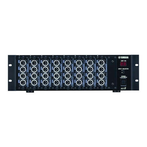
SPECIFICATIONS Sampling frequency (external sync) 39.69 kHz – 50.88 kHz USA and Canada: 120 V, 60 Hz Power supply Others: 230 V, 50 Hz Power consumption 120 W Dimensions (W x H x D) 480 mm x 141.5 mm x 466.8 mm Weight 15.4 kg Operating temperature... - Page 6 OUTPUT UNIT ID Front Panel INPUT SELECTOR UNIT NO. INPUT SELECTOR POWER POWER ANALOG OUTPUT BOX The illustration shows the AO8 analog output box. ANALOG OUTPUT BOX OUTPUT UNIT ID indicator INPUT SELECTOR switch POWER ON/OFF Rear Panel INPUT WORD...
- Page 7 DIMENSIONS OUTPUT UNIT ID INPUT SELECTOR POWER ANALOG OUTPUT BOX Unit: mm...
-
Page 8: Connector Circuit Diagram
CONNECTOR CIRCUIT DIAGRAM LED2 IPC4 IPC2 IPC2 IFC3 KEC-92523-2... - Page 9 Circuit Board CN No. Pin No. Circuit Board CN No. Pin No. CN100 CN122 CN124 CN127 IFC3 CN104 CN122 CN124 CN127 IFC3 CN104 CN101 CN127 IFC3 CN104 CN200 CN121 CN123 CN125 CN121 CN123 CN125 CN201 CN121 CN123 CN125 CN300 CN500 CN301 CN122 CN124...
- Page 10 SLOT No. [INPUT] /CS1 /CON1 IC401 DIR2 /CS2 Driver /CON2 Receiver INPUT CLOCK ID I/O ATSC INPUT CLOCK IC301 IPC2 /CS3 44.1K DIR2 /CON3 IC501 IC402 IC502 /CS4 DIR2 LOCK /CON4 Driver WC SEL & SYNC DETECTOR Receiver ID I/O SELECTOR /CS5 IPC2...
-
Page 11: Disassembly Procedure
DISASSEMBLY PROCEDURE UNC Card Assembly Remove the four (4) screws marked [470]. The UNC card assembly can them be removed. (Fig. 1) Front Panel Assembly Remove the UNC card assembly. (See Procedure 1.) Remove the thirty-two (32) screws marked [500]. The blank panel can then be removed. - Page 12 [170] <Top View> [430] x 17 LED2 [80] [100] Top panel [80]: Bind Head Tapping Screw-B 3.0x6 MFZN2BL (EP600230) [100]: Bind Head Screw 3.0x8 MFZN2BL (VB659000) [170]: Bind Head Tapping Screw-B A4.0x8 MFZN2BL (VC688800) [430]: Bind Head Tapping Screw-B A4.0x8 MFZN2BL (VC688800) Fig.
- Page 13 MB1 Circuit Board Remove the mother assembly. (See Procedure 6.) Remove the nine (9) screws marked [30] and the five (5) screws marked [50]. The MB1 circuit board can then be removed. (Fig. 4) IFC3 Circuit Board Remove the mother assembly. (See Procedure 6.) Remove the six (6) screws marked [70].
- Page 14 AC Assembly 10-1 Remove the side panel assembly. (See Procedure 9.) 10-2 Remove the three (3) screws marked [90]. The AC assembly can then be removed. (Fig. 6) DC Assembly 11-1 Remove the side panel assembly. (See Procedure 9.) 11-2 Remove the four (4) screws marked [60].
-
Page 15: Lsi Pin Description
LSI PIN DESCRIPTION SGH609080F-47F (XU235A00) ATSC IFC3: IC501–504 NAME FUNCTION NAME FUNCTION syncati Synch. word input terminal for ati, synci Synch. word input terminal for si3-0 input siat3-0 input mccti 64 fs clock input terminal for ati, mcci 64 fs clock input terminal for si3-0 input siat3-0 input mcbti 128 fs clock input terminal for ati,... - Page 16 YM3436DK (XG948E0) DIR2 (Digital Format Interface Receiver) IFC3: IC301 to 303, 401 to 403 NAME FUNCTION NAME FUNCTION DAUX Auxiliary input for audio data RSTN System reset input HDLT Asynchronous buffer operation flag Vdda VCO section power (+5V) DOUT Audio data output CTLN VCO control input N Parity flag output...
- Page 17 HD6477042AF28 (XY715A00) CPU UNC: IC101 NAME FUNCTION NAME FUNCTION PE14 Port E PE15 Port E Data bus Ground Ground Data bus Power supply Address bus Data bus Ground XTAL Crystal oscillator Mode control EXTAL Crystal oscillator Mode control Non-maskable interrupt request Power supply Power supply Address bus...
-
Page 18: Ic Block Diagram
IC BLOCK DIAGRAM HD74LVU04AFPEL (XY102A00) HD74LV04AFPEL (IS000400) HD74LV08AFPEL (IS000800) Hex Inverter Hex Inverter Quad 2 Input AND IFC3: IC105 IFC3: IC311, 408 IFC3: IC104, 310, 409 UNC: IC105 UNC: IC104, 213 SN74LV138ANSR (IS013810) TC74VHC245F (XT487A00) DS26C32ATMX (XU815A00) 3 to 8 Demultiplexer Octal 3-State Bus Transceiver Quad Differential Line Receiver UNC: IC211, 212... -
Page 19: Ipc2 Circuit Board (Xw289A0)
CIRCUIT BOARDS AC Circuit Board (XW295B0)····················································································· 16 DC Circuit Board (XW295B0)····················································································· 17 DR Circuit Board (XW295B0)····················································································· 16 IFC3 Circuit Board (XW287A0) ·················································································· 19 IPC2 Circuit Board (XW289A0) ·················································································· 15 IPC4 Circuit Board (XW286B0) ·················································································· 16 LED2 Circuit Board (XW286B0)················································································· 16 MB1 Circuit Board (XW282A0) ··················································································... -
Page 20: Ac Circuit Board (Xw295B0)
AC Circuit Board DR Circuit Board Component side PSB Circuit Board POWER ON/OFF to PSB-CN600 Power transformer Component side IPC4 Circuit Board Component side LED2 Circuit Board INPUT SELECTOR A/B Component side AC, DR, PSB: 3NA-V412970 Component side IPC4, LED2: 3NA-V491380... -
Page 21: Dc Circuit Board (Xw295B0)
to DC-CN100 to DC-CN100 to DC-CN100 to DC-CN200 CN301 to DC-CN200 CN301 to DC-CN200 CN101 CN201 CN303 CN201 CN303 CN201 to DC-CN301 CN302 to IFC3-CN408 to IFC3-CN407 to IFC3-CN406 to IFC3-CN405 to IFC3-CN404 to IFC3-CN403 to IFC3-CN402 to IFC3-CN401 to MB1-CN122 to MB1-CN121 CN124 CN123... -
Page 22: Unc Circuit Board (Xw281B0)
UNC Circuit Board Pattern side Component side 3NA-V412870... -
Page 23: Ifc3 Circuit Board (Xw287A0)
to IPC2 2/2-CN101 to DC-CN100 to MB1-CN119 to IPC2 2/2-CN102 to IPC2 1/2-CN102 to LED1-CN100 CN101 to MB1-CN117 to MB1-CN116 to MB1-CN115 to MB1-CN114 to MB1 to MB1-CN112 to IPC4 to IPC2 2/2 to MB1-CN110 -CN113 -CN300 -CN104 to MB1-CN120 to MB1-CN111 to IPC2 2/2 to IPC2 1/2-CN104... -
Page 24: Inspection
Power speaker Power speaker Power speaker Power speaker Power speaker · Set the AI8 and AO8 sheet UNC DIP switch as below. DIP Switch 8 is not used. DIP SW DIP SW DIP SW DIP SW · For 01V, OSC1kHz is output from OMNI1 OUT and the signal input to INPUT is assigned to ST OUT. -
Page 25: Test Program
(It is good if the wave form like the one shown in Figure 1 appears.) Observe at the time of completing the inspection of Port A of the AO8-IPC 2 Test. Observe at the time of completing the inspection of Port B of the AO8-IPC 2 Test. - Page 26 5. After writing ends, end PM1DLOAD. 6. Switch off the power for AO8 and remove the PH connector, then switch the power for AO8. DSP1D on again and check that it starts up normally. (Operation is normal if an "...
- Page 27 Overall Inspection Specifications. Install the inspection jig to the AO8 to be inspected as in the figure above. Send the inspection commands from the PC via the AI8 to the LMY-slot inspection jig and take in at the PC the results returned from the LMY-slot inspection jig.
- Page 28 NG: LED flashes on (0.1 s) - Off (0.1 s) - On (0.1 s) - Off (0.1 s) AO8 - IFC3 Test This test checks around the AO8-IFC3. NG sample Please refer to the AO8-UNC Test for NG charts. 2. AO8-IFC3 Test 2. AO8-IFC3 Test * SICKB...
- Page 29 The detected voltage is displayed and the percentage deviation from the ideal state is displayed. This is shown for each slot. 3-2. AO8 - Slot [Clock Line] Test This test checks around the slot clock. NG example 3-2. AO8-SLOT [Clock Line] Test OK 3-2.
- Page 30 0.0. 1.1 .2.2. · · · 9.9. AO8 - IPC2 test This test checks around the AO8 - IPC2. Ports A and B are both checked, so the same procedure is carried out in 5-1 for Port A and in 5-2 for Port B.
-
Page 31: Error Messages
ERROR MESSAGE DESCRIPTION The AO8 is connected to the INPUT connector of the DSP1D/DSP1D-EX. Connect the AO8 to the OUTPUT connector. A cable is disconnected from the INPUT A, B, or C connector on the rear panel, or the connection is made incorrectly. -
Page 32: Specifications
ANALOG OUTPUT BOX PARTS LIST CONTENTS OVERALL ASSEMBLY······························································································································ 2 SIDE PANEL ASSEMBLY ························································································································· 4 MOTHER ASSEMBLY······························································································································· 6 ELECTRICAL PARTS ························································································································· 7~12 Notes : DESTINATION ABBREVIATIONS Australian model M: South African model British model Chinese model Canadian model South-east Asia model German model Taiwan model European model... - Page 33 OVERALL ASSEMBLY 390b 390a 390c 460a 460b 460c...
-
Page 34: Circuit Boards
4.0X12 MFZN2BL V4278900 PET Sheet Front Shassis V4277800 VC688800 Bind Head Tapping Screw-B A4.0X8 MFZN2BL V49136S0 Circuit Board AO8 LED2 (IPCOM) EP600230 Bind Head Tapping Screw-B 3.0X6 MFZN2BL Circuit Board AO8 PSB (AOCOM) V49137S0 VB659000 Bind Head Screw 3.0X8 MFZN2BL... - Page 35 PART NO. DESCRIPTION REMARKS REF NO. RANK VS863000 Bonding Screw 3.0X6 MFZN2BL Label, Caution (V533510) Blank Panel V4278500 VS863000 Bonding Screw 3.0X6 MFZN2BL CB835590 Holder TMS-20 CB069250 Cord Holder BK-1 VC362700 Ferrite Core FR25/15/12-1400L Connector Assembly Earth #18 (V572480) VP156800 Bind Head Screw A4.0X8 MFZN2BL VY734700...
-
Page 36: Circuit Boards
Bind Head Screw A4.0X6 MFZN2BL V5099200 Connector Assembly PH-DC AC Assembly J,U,V (V479470) AC Assembly H,B,W (V479480) V46487S0 Circuit Board AO8 AC (AOCOM) KB003620 Fuse 4.00A JU J,U,V KB003090 Fuse 3.15A S H,B,W VC688800 Bind Head Tapping Screw-B A4.0X8 MFZN2BL Ferrite Core... -
Page 37: Ifc3
Support Metal EP600230 Bind Head Tapping Screw-B 3.0X6 MFZN2BL V4278100 Support Metal EP600230 Bind Head Tapping Screw-B 3.0X6 MFZN2BL V41300S0 Circuit Board AO8 IFC3 CB817510 Cord Binder S-14B EP600230 Bind Head Tapping Screw-B 3.0X6 MFZN2BL Cable, FFC P=1.25-K-20-80 (V508550) Cable, FFC P=1.25-K-30-80... -
Page 38: Electrical Parts
ELECTRICAL PARTS PART NO. DESCRIPTION REMARKS REF NO. RANK ELECTRICAL PARTS V46487S0 Circuit Board AO8 AC (AOCOM) (XW295C0) V46490S0 Circuit Board AO8 DC (AOCOM) (XW295C0) V46492S0 Circuit Board AO8 DR (AOCOM) (XW295C0) V49137S0 Circuit Board AO8 PSB (AOCOM) (XW295C0) V41302S0... - Page 39 Transistor 2SC1815 Y,GR ZD500 VQ554100 Zener Diode MTZJ7.5A 7.5V W0013 GND Wire L=180 (V744560) V41302S0 Circuit Board AO8 IPC2 (XW289A0) C108 UF038100 Electrolytic Cap. (chip) 100 16V UB245100 Monolithic Ceramic Cap. F 0.100 25V Z CN100 V4158600 Connector 230R(SCSI) 68P SE...
- Page 40 Carbon Resistor (chip) 10.0K 0.1 J RD257220 Carbon Resistor (chip) 22.0K 0.1 J RD257470 Carbon Resistor (chip) 47.0K 0.1 J V41300S0 Circuit Board AO8 IFC3 (XW287B0) C112 UF038100 Electrolytic Cap. (chip) 100 16V C116 UF017220 Electrolytic Cap. (chip) 22 6.3V C118 Electrolytic Cap.
- Page 41 RD258910 Carbon Resistor (chip) 910.0K 0.1 J RD259100 Carbon Resistor (chip) 1.0M 0.1 J RD259300 Carbon Resistor (chip) 3.0M 0.1 J Circuit Board AO8 IPC4 (IPCOM) (XW286B0) V41293S0 V49136S0 Circuit Board AO8 LED2 (IPCOM) (XW286B0) C304 UR838100 Electrolytic Cap. 100.00 16.0V...
- Page 42 PART NO. DESCRIPTION REMARKS REF NO. RANK V41288S0 Circuit Board AI8 MB1 (XW282A0) CN101 VU328200 Plug PHEC 100P TE SLOT 1-8,UNC Card -109 VU328200 Plug PHEC 100P TE CN110 VI878600 Cable Holder 51048 8P TE -117 VI878600 Cable Holder 51048 8P TE CN118 VI878400 Cable Holder...
- Page 43 PART NO. DESCRIPTION REMARKS REF NO. RANK FZ200 Fuse 5.00A JU J,U,V KB003630 FZ200 KB003100 Fuse 4.00A S H,B,W FZ201 KB003630 Fuse 5.00A JU J,U,V FZ201 KB003100 Fuse 4.00A S H,B,W FZ300 KB003630 Fuse 5.00A JU J,U,V FZ300 KB003100 Fuse 4.00A S H,B,W FZ301...
-
Page 44: Circuit Diagram
ANALOG OUTPUT BOX CIRCUIT DIAGRAM CONTENTS UNC ···································································· 3 MB1····································································· 5 IFC3 ···································································· 9 IPC2 ·································································· 15 IPC4 ·································································· 16 LED2 ································································· 17 AOCOM ···························································· 18 WARNING Components having special characteristics are marked and must be replaced with parts having specification equal to those originally installed. -
Page 45: Unc
UNC CIRCUIT DIAGRAM 002 ( AO8 ) SYSTEM RESET TRANSCEIVER INVERTER INVERTER : Ceramic Capacitor UNC CIRCUIT DIAGRAM 002 ( AO8 ) KEC-92504-2... -
Page 46: Circuit Diagram
UNC CIRCUIT DIAGRAM 003 ( AO8 ) TRANSCEIVER FLASH MEMORY 4M SRAM 1M DECODER DECODER TRANSCEIVER : Ceramic Capacitor UNC CIRCUIT DIAGRAM 003 ( AO8 ) KEC-92504-3... -
Page 47: Mb1
MB1 CIRCUIT DIAGRAM 002 ( AO8 ) MB1 CIRCUIT DIAGRAM 002 ( AO8 ) KEC-92505-2... -
Page 48: Circuit Diagram
MB1 CIRCUIT DIAGRAM 003 ( AO8 ) MB1 CIRCUIT DIAGRAM 003 ( AO8 ) KEC-92504-3... -
Page 49: Circuit Diagram
MB1 CIRCUIT DIAGRAM 004 ( AO8 ) MB1 CIRCUIT DIAGRAM 004 ( AO8 ) KEC-92505-4... -
Page 50: Circuit Diagram
MB1 CIRCUIT DIAGRAM 005 ( AO8 ) to IFC3-CN105 to IFC3-CN505 to IFC3-CN501 from DC-CN200-1,2,7p from DC-CN100-1,2,8,9p -CN301-1p to IFC3-CN506 to IFC3-CN502 to IFC3-CN101 from DC-CN200-3,4,8p to IFC3-CN503 to IFC3-CN507 from DC-CN100-3,4,10,11p -CN301-2p from DC-CN200-5,6,9p to IFC3-CN102 to IFC3-CN508 to IFC3-CN504... -
Page 51: Circuit Diagram
IFC3 CIRCUIT DIAGRAM 002 ( AO8 ) from IPC-CN300 from MB1-CN119 TRANSCEIVER TRANSCEIVER from MB1-CN118 TRANSCEIVER TRANSCEIVER from MB1-CN120 REGULATOR from DC-CN100-6,7,13,14p -CN101-2,3p TRANSCEIVER INVERTER to LED2-CN100 INVERTER INVERTER IFC3 CIRCUIT DIAGRAM 002 ( AO8 ) KEC-92510-2... -
Page 52: Circuit Diagram
IFC3 CIRCUIT DIAGRAM 003 ( AO8 ) FPGA EPROM 1M IFC3 CIRCUIT DIAGRAM 003 ( AO8 ) KEC-92510-3... -
Page 53: Circuit Diagram
IFC3 CIRCUIT DIAGRAM 004 ( AO8 ) DIR2 DIR2 INVERTER INVERTER INVERTER DIR2 SYSTEM RESET INVERTER INVERTER : Mylar Capacitor IFC3 CIRCUIT DIAGRAM 004 ( AO8 ) KEC-92510-4... -
Page 54: Circuit Diagram
IFC3 CIRCUIT DIAGRAM 005 ( AO8 ) TRANSCEIVER INVERTER DIR2 to MB1-CN117 SYSTEM RESET TRANSCEIVER to MB1-CN116 INVERTER to MB1-CN115 TRANSCEIVER to MB1-CN114 INVERTER DIR2 to MB1-CN113 SYSTEM RESET to MB1-CN112 TRANSCEIVER INVERTER to MB1-CN111 TRANSCEIVER to MB1-CN110 INVERTER DIR2... -
Page 55: Circuit Diagram
IFC3 CIRCUIT DIAGRAM 006 ( AO8 ) ATSC ATSC ATSC ATSC IFC3 CIRCUIT DIAGRAM 006 ( AO8 ) KEC-92510-6... -
Page 56: Circuit Diagram
IFC3 CIRCUIT DIAGRAM 007 ( AO8 ) from IPC2-CN101 from IPC2-CN101 TRANSCEIVER TRANSCEIVER from IPC2-CN102 from IPC2-CN102 TRANSCEIVER TRANSCEIVER from IPC2-CN103 from IPC2-CN103 TRANSCEIVER TRANSCEIVER from IPC2-CN104 from IPC2-CN104 TRANSCEIVER TRANSCEIVER IFC3 CIRCUIT DIAGRAM 007 ( AO8 ) KEC-92510-7... -
Page 57: Ipc2
IPC2 CIRCUIT DIAGRAM ( AO8 ) LINE RECEIVER LINE RECEIVER to IFC3-CN601 -CN605 LINE RECEIVER to IFC3-CN602 -CN606 LINE DRIVER LINE RECEIVER to IFC3-CN603 -CN607 LINE RECEIVER TRANSCEIVER to IFC3-CN604 -CN608 TRANSCEIVER : not Installed IPC2 CIRCUIT DIAGRAM ( AO8 ) -
Page 58: Ipc4
IPC4 CIRCUIT DIAGRAM ( AO8 ) LINE RECEIVER to IFC3-CN106 LINE DRIVER IPC4 CIRCUIT DIAGRAM ( AO8 ) KEC-92508-2... -
Page 59: Led2
LED2 CIRCUIT DIAGRAM ( AO8 ) from IFC3-CN103 LED2 CIRCUIT DIAGRAM ( AO8 ) KEC-92512-2... -
Page 60: Aocom
AOCOM CIRCUIT DIAGRAM 002 ( AO8 ) REGULATOR +5V 2A to MB1-CN122-1,2,3,4p -CN124-1,2,3,4p REGULATOR +5V 2A -CN127-3,4,5p IFC3-CN104 REGULATOR +3.3V to MB1-CN127-4p IFC3-CN104-5,6p REGULATOR +5V 2A REGULATOR +5V REGULATOR +5V REGULATOR +5V to MB1-CN121-1,4p -CN123-1,4p -CN125-1,4p to MB1-CN121-2p -CN123-2p REGULATOR -5V... -
Page 61: Circuit Diagram
1: INPUT 1: INPUT 3: GND 2: GND 2: COMMON 2: COMMON 2: INPUT 2: COMMON 2: INPUT 3: IN 4: ON/OFcont. 3: OUTPUT 3: OUTPUT 3: OUTPUT 3: COMMON 3: COMMON AOCOM CIRCUIT DIAGRAM 003 ( AO8 ) KEC-92513-3...