Table of Contents
Advertisement
Quick Links
Download this manual
See also:
Owner's Manual
DA CONVERTER
SERVICE MANUAL
CONTENTS
SPECIFICATIONS ···································································· 3
PANEL LAYOUT······································································· 4
CIRCUIT BOARD LAYOUT ······················································ 5
DIMENTIONS ··········································································· 6
BLOCK DIAGRAM ···································································· 7
DISASSEMBLY PROCEDURE················································· 8
LSI PIN DESCRIPTION ·························································· 11
IC BLOCK DIAGRAM ····························································· 13
CIRCUIT BOARDS ································································· 15
INSPECTIONS········································································ 27
TEST PROGRAM ··································································· 29
FRASH ROM UPGRADE························································ 32
PARTS LIST
OVERALL CIRCUIT DIAGRAM
This document is printed on chlorine free (ECF) paper with soy ink.
PA
011524
HAMAMATSU, JAPAN
200005**-110000
1.44K-4111 K
Printed in Japan '00.05
Advertisement
Table of Contents

Related Manuals for Yamaha DA824


Summary of Contents for Yamaha DA824
- Page 1 DA CONVERTER SERVICE MANUAL CONTENTS SPECIFICATIONS ···································································· 3 PANEL LAYOUT······································································· 4 CIRCUIT BOARD LAYOUT ······················································ 5 DIMENTIONS ··········································································· 6 BLOCK DIAGRAM ···································································· 7 DISASSEMBLY PROCEDURE················································· 8 LSI PIN DESCRIPTION ·························································· 11 IC BLOCK DIAGRAM ····························································· 13 CIRCUIT BOARDS ································································· 15 INSPECTIONS········································································...
- Page 2 IMPORTANT NOTICE This manual has been provided for the use of authorized Yamaha Retailers and their service personnel. It has been assumed that basic service procedures inherent to the industry, and more specifically Yamaha Products, are already known and understood by the users, and have therefore not been restated.
-
Page 3: Specifications
DA824 SPECIFICATIONS MY8-AE, MY8-TD 39.69–50.88 kHz Sampling rate MY8-AT 41.013–50.88 kHz DA conversion resolution 24-bit linear, 128-times oversampling Frequency response –3, +1 dB, 20 Hz–20 kHz Dynamic Range * 110 dB (typical) ±1 dB @ 1 kHz Gain Error 0.05%, 20 Hz–20 kHz THD * 0.01% full scale output @ 1 kHz... -
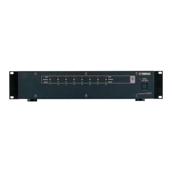
Page 4: Panel Layout
1 PEAK, NOMINAL & SIGNAL indicators 2 LOCK indicator 3 POWER indicator 4 POWER switch Rear Panel DA CONVERTER WORD CLOCK OUTPUT MODEL DA824 (BAL) THRU ON OFF SLOT 5 COM port 6 WORD CLOCK THRU connector 7 WORD CLOCK 75... -
Page 5: Circuit Board Layout
DA824 CIRCUIT BOARD LAYOUT CN052 CN053 CN051 CN054 MYSL CN101 CN301 CN501 CN701 CN102 CN302 CN502 CN702 CN003 CN004 MAIN MYSL CN902 CN002 CN001 CN905 CN901 CN906 CN003 CN011 CN010 CN008 CN007 Power Transformer CN962 CN961 3NC2-V536450... -
Page 6: Dimentions
DA824 DIMENTIONS W: 480 H: 97.5 Unit: mm 67.5 67.5... -
Page 7: Block Diagram
DA824 BLOCK DIAGRAM WORD CLOCK IC902 IC917 IC918 WORD CLOCL WORD CLOCL 6~10 SELECT SELECT IC923 THRU YM3436DK YM3436DK (DIR2) (DIR2) LOCK DA JK PEAK 24dBU SYNC.Fs.64Fs.128Fs.256Fs 18dBU NOMINAL IC103 JK101 15dBU SIGNAL +4dBV MUTE VOUTL OUTPUT 1 MUTE IC002... -
Page 8: Disassembly Procedure
DA824 DISASSEMBLY PROCEDURE Top Cover Remove the fourteen (14) screws marked [400]. The top cover can then be removed. (Fig. 1) Circuit Boards and Units Remove the top cover, each circuit board and unit can then be removed. Circuit Board and Unit Ref. - Page 9 DA824 AC Circuit Board Remove the top cover. (See procedure 1.) Remove the three (3) screws marked [60A] and the two (2) screws marked [110]. The AC circuit board can then be removed. (Fig. 4) The fuse is not a part of the AC circuit Board. When you...
- Page 10 DA824 PN Circuit Board: Remove the four (4) screws marked [30]. The PN circuit board can then be removed. (Fig. 7) SW Circuit Board: Remove the two (2) screws marked [50]. The SW circuit board can then be removed. (Fig. 7) •...
-
Page 11: Lsi Pin Description
DA824 LSI PIN DESCRIPTION YM3436DK (XG948E00) DIR2 (Digital Format Interface Receiver) MAIN: IC917, 918 NAME FUNCTION NAME FUNCTION DAUX Auxiliary input for audio data RSTN System reset input HDLT Asynchronous buffer operation flag Vdda VCO section power (+5V) DOUT Audio data output... - Page 12 DA824 HD6477042AF28 (XY721A00) CPU MAIN: IC909 NAME FUNCTION NAME FUNCTION PE14 Port E PE15 Port E Data bus Ground Ground Data bus Power supply Address bus Data bus Ground XTAL Crystal oscillator Mode control EXTAL Crystal oscillator Mode control Non-maskable interrupt request...
-
Page 13: Ic Block Diagram
DA824 IC BLOCK DIAGRAM HD74LV04AFPEL (IS000400) HD74LV08AFPEL (IS000800) HD74LV32AFPEL (IS003200) HD74LVU04AFPEL (XY102A00) Quad 2 Input AND Quad 2 Input OR Hex Inverter MAIN: IC912 MAIN: IC928 MAIN: IC911,915 HD74LV74AFPEL (IS007400) SN74LV138ANSR (IS013810) SN74LV139ANSR (IS013910) Dual D-Type Flip-Flop 3 to 8 Demultiplexer... - Page 14 DA824 SN75121NSR (XU816A00) SN75124NS (XN976A00) SN75C1168NSR (XU073A00) Dual Line Driver Triple Line Receiver Line Driver / Receiver MAIN: IC923 MAIN: IC902 MAIN: IC906 NJM2068D-D (XA987A00) NJM2068MD-T1 (XJ553A00) NJM4556AL (XP844A00) Dual Operational Amplifier PN: IC101,301,501,701 DA: IC101-103,201-203,301-303,401-403, 501-503,601-603,701-703,801-803 +DC Voltage Output A...
-
Page 15: Circuit Boards
DA824 CIRCUIT BOARDS AC Circuit Board (H,W,B) (XY032C0) ······································································· 15 AC Circuit Board (J, U, V) (XY031C0) ······································································· 15 DA Circuit Board (XY035B0)······················································································ 23 DC Circuit Board (H,W,B) (XY032C0) ······································································· 17 DC Circuit Board (J, U, V) (XY031C0) ······································································· 16 JK Circuit Board (XY035B0) ······················································································... - Page 16 DA824 DC Circuit Board (J, U, C) Power transformer Power transformer to MYSL-CN052 to MAIN-CN905 to PN-CN963 to DA-CN001 Component side 3NA-V485500...
- Page 17 DA824 DC Circuit Board (H,W,B) Power transformer Power transformer to MYSL-CN052 to MAIN-CN905 to PN-CN963 to DA-CN001 Component side 3NA-V485540...
- Page 18 DA824 PN Circuit Board from DC-CN009 Component side 3NA-V485460...
- Page 19 DA824 MAIN Circuit Board WORD CLOCK THRU to DA-CN003 from DC-CN010 to MYSL-CN054 to MYSL-CN053 3NA-V485480...
- Page 20 DA824 MYSL Circuit Board from DC-CN008 from MAIN-CN902 from MAIN-CN901 Component side to PN-CN961 Component side MAIN,MYSL: 3NA-V485480...
- Page 21 DA824 MAIN Circuit Board 3NA-V485480...
- Page 22 DA824 MYSL Circuit Board Pattern side Pattern side MAIN,MYSL: 3NA-V485480...
- Page 23 DA824 DA Circuit Board OUTPUT to JK-CN301 to JK-CN301 to JK-CN501 to PN-CN962 to DC-CN011 3NA-V485470...
- Page 24 DA824 JK Circuit Board OUTPUT to JK-CN701 from MAIN-CN904 Component side Component side DA, JK: 3NA-V485470...
- Page 25 DA824 DA Circuit Board 3NA-V485470...
- Page 26 DA824 JK Circuit Board Pattern side Pattern side DA, JK: 3NA-V485470...
-
Page 27: Inspections
DA824 INSPECTION Preparations · 0 dBu=0.775 Vrms · 0 dBV-1 Vrms=2.2 dBu · The output impedance of the oscillator connected is 150 ohms. · The input impedance of the oscilloscope and the level meter should be more than 100 k ohms. - Page 28 -18 dBu Jitter measurement · Connect AD824 word clock out and DA824 word clock in. · Insert MY8-AE card into the slot and connect to DSA1 via the D-sub-cannon converter box. · Set AD824 word clock settings to 48 kHz and 44.1 kHz.
-
Page 29: Test Program
DA824_DIAG> and the DA824 will enter the test program mode. The version of the test program will be shown as x.xx. To remove the test program mode, enter "reset". It will be displayed as followed and it will be the same as when the power is turned on. - Page 30 DA824 Automatic inspection Use the keyboard for the PC to enter "test" and execute program DA824_DIAG>test The following items will be inspected automatically. At the end, a list of items determined to be NG (no good) will be displayed on the screen.
-
Page 31: System Reset
DA824 Slot power supply peripheral connection check Only the NG systems from the test results will be shown on the screen. [5] WC BNC Displayed on the screen when the results of the word clock IN terminal/ JK901 and CPU connection are NG. - Page 32 1. Connection Click the [Browse] switch and the following window will Connect the PC and DA824 COM terminals by Dsub 9 pin open. Designate the files to be loaded to the DA824 and click serial cross cables. the [Open] switch.
-
Page 33: Table Of Contents
DA CONVERTER PARTS LIST CONTENTS OVERALL ASSEMBLY······························································································································ 2 FRONT PANEL ASSEMBLY ····················································································································· 4 REAR PANEL ASSEMBLY ······················································································································· 5 DC ASSEMBLY ········································································································································· 6 ELECTRICAL PARTS ························································································································· 7~21 Notes: DESTINATION ABBREVIATIONS Australian model M: South African model British model Chinese model Canadian model South-east Asia model German model Taiwan model... -
Page 34: Overall Assembly
DA824 OVERALL ASSEMBLY Rear panel assembly: See page 5 210 250 DC assembly: See page 6 Front panel assembly: See page 4... - Page 35 DA824 PART NO. DESCRIPTION REMARKS REF NO. RANK OVERALL ASSEMBLY DA824 Overall Assembly (V536450) Overall Assembly (V536470) Overall Assembly (V536480) Overall Assembly (V536490) V4067500 Bottom Chassis Label H,W,B (V567270) CB806590 VR138400 Bind Head Tapping Screw-B 4.0X12 MFZN2BL Protection Sheet (V553110)
-
Page 36: Front Panel Assembly
DA824 FRONT PANEL ASSEMBLY PART NO. DESCRIPTION REMARKS REF NO. RANK FRONT PANEL ASSEMBLY DA824 Front Panel Assembly J,U,V (V545270) Front Panel Assembly H,W,B (V561280) V4067800 Sub Chassis V4854600 Circuit Board EP600230 Bind Head Tapping Screw-B 3.0X6 MFZN2BL V4855300 Circuit Board... -
Page 37: Rear Panel Assembly
DA824 REAR PANEL ASSEMBLY PART NO. DESCRIPTION REMARKS REF NO. RANK REAR PANEL ASSEMBLY DA824 Rear Panel Assembly (V545160) Rear Panel Assembly (V545170) Rear Panel Assembly (V545180) Rear Panel Assembly (V545190) V6035200 Rear Panel V5254400 Rear Panel V5254500 Rear Panel... -
Page 38: Dc Assembly
DA824 DC ASSEMBLY PART NO. DESCRIPTION REMARKS REF NO. RANK DC ASSEMBLY DA824 V5452300 DC Assembly J,U,V V5452500 DC Assembly H,W,B Heat Sink (V406870) V4068800 Insulation Sheet V4855200 Circuit Board J,U,V V4855600 Circuit Board H,W,B VN413300 Bonding Tapping Screw-B 3.0X8 MFZN2BL... -
Page 39: Electrical Parts
DA824 ELECTRICAL PARTS PART NO. DESCRIPTION REMARKS REF NO. RANK ELECTRICAL PARTS DA824 V4855100 Circuit Board J,U,V (XY031C0) V4855500 Circuit Board H,W,B (XY032C0) V4855200 Circuit Board J,U,V (XY031C0) V4855600 Circuit Board H,W,B (XY032C0) V4855300 Circuit Board J,U,V (XY031C0) V4855700 Circuit Board... - Page 40 DA824 PART NO. DESCRIPTION REMARKS REF NO. RANK VP206500 Fuse Holder EYF-52BC VP206500 Fuse Holder EYF-52BC XJ603A00 NJM78M15FA REGULATOR +15V 0.5A XG505A00 NJM79M15FA REGULATOR -15V XR607A00 UPC2405AHF REGULATOR +5V XK309A00 NJM7905FA REGULATOR -5V XH672A00 PQ05RF2 REGULATOR +5V 2A XD631A00 PST518B-TP...
- Page 41 DA824 PART NO. DESCRIPTION REMARKS REF NO. RANK UU167100 Electrolytic Cap. 10.00 50.0V UB245100 Monolithic Ceramic Cap. F 0.100 25V Z UB245100 Monolithic Ceramic Cap. F 0.100 25V Z UB245220 Monolithic Ceramic Cap. F 0.220 25V Z UB245220 Monolithic Ceramic Cap.
- Page 42 DA824 PART NO. DESCRIPTION REMARKS REF NO. RANK C603 UB051330 Monolithic Ceramic Cap. SL 33P 50V J C604 UB051330 Monolithic Ceramic Cap. SL 33P 50V J C605 UA353680 Mylar Capacitor 6800P 50V J C606 UA353300 Mylar Capacitor 3000P 50V J...
- Page 43 DA824 PART NO. DESCRIPTION REMARKS REF NO. RANK XW029A00 AK4393-VF-E2 XJ598A00 NJM78L05UA REGULATOR +5V XJ598A00 NJM78L05UA REGULATOR +5V IC101 XJ553A00 NJM2068MD-T1 OP AMP IC102 XJ553A00 NJM2068MD-T1 OP AMP IC103 XP844A00 NJM4556AL OP AMP IC201 XJ553A00 NJM2068MD-T1 OP AMP IC202 XJ553A00...
- Page 44 DA824 PART NO. DESCRIPTION REMARKS REF NO. RANK R120 VC328800 Metal Film Resistor 10.0K 1/4 F R121 VC329500 Metal Film Resistor 20.0K 1/4 F R122 VC329500 Metal Film Resistor 20.0K 1/4 F R123 VC329400 Metal Film Resistor 18.0K 1/4 F...
- Page 45 DA824 PART NO. DESCRIPTION REMARKS REF NO. RANK R330 RD257100 Carbon Resistor (chip) 10.0K 0.1 J R401 VC327600 Metal Film Resistor 3.3K 1/4 F R402 VC327600 Metal Film Resistor 3.3K 1/4 F R403 VC329200 Metal Film Resistor 15.0K 1/4 F...
- Page 46 DA824 PART NO. DESCRIPTION REMARKS REF NO. RANK R610 VC328500 Metal Film Resistor 7.5K 1/4 F R611 VC330500 Metal Film Resistor 51.0K 1/4 F R612 VC329600 Metal Film Resistor 22.0K 1/4 F R613 VC327100 Metal Film Resistor 2.0K 1/4 F...
- Page 47 DA824 PART NO. DESCRIPTION REMARKS REF NO. RANK R820 VC328800 Metal Film Resistor 10.0K 1/4 F R821 VC329500 Metal Film Resistor 20.0K 1/4 F R822 VC329500 Metal Film Resistor 20.0K 1/4 F R823 VC329400 Metal Film Resistor 18.0K 1/4 F...
- Page 48 DA824 PART NO. DESCRIPTION REMARKS REF NO. RANK -946 UB245100 Monolithic Ceramic Cap. F 0.100 25V Z C947 VR327300 Mylar Capacitor (chip) 0.0820 16V J C950 VR327300 Mylar Capacitor (chip) 0.0820 16V J CN51 VU328200 Plug PHEC 100P TE SLOT...
- Page 49 DA824 PART NO. DESCRIPTION REMARKS REF NO. RANK R912 RD259100 Carbon Resistor (chip) 1.0M 0.1 J R913 RD256200 Carbon Resistor (chip) 2.0K 0.1 J R914 RD256200 Carbon Resistor (chip) 2.0K 0.1 J R917 RD256220 Carbon Resistor (chip) 2.2K 0.1 J...
- Page 50 DA824 PART NO. DESCRIPTION REMARKS REF NO. RANK D601 VB941200 Diode 1SS133,1SS176 D602 VB941200 Diode 1SS133,1SS176 D701 VB941200 Diode 1SS133,1SS176 D702 VB941200 Diode 1SS133,1SS176 D801 VB941200 Diode 1SS133,1SS176 D802 VB941200 Diode 1SS133,1SS176 EM960 FZ006970 LC Filter LS MT Y223NB -962...
- Page 51 DA824 PART NO. DESCRIPTION REMARKS REF NO. RANK R303 VC331200 Metal Film Resistor 100K 1/4 F R304 VC328700 Metal Film Resistor 9.1K 1/4 F R305 VC331200 Metal Film Resistor 100K 1/4 F R306 VC330300 Metal Film Resistor 43.0K 1/4 F...
- Page 52 DA824 PART NO. DESCRIPTION REMARKS REF NO. RANK -716 HF757470 Carbon Resistor 47.0K 1/4 J R717 HF755390 Carbon Resistor 390.0 1/4 J -719 HF755390 Carbon Resistor 390.0 1/4 J R801 VC330800 Metal Film Resistor 68.0K 1/4 F R802 VB070300 Metal Film Resistor 200.0K 1/5 F...
- Page 53 DA824 PART NO. DESCRIPTION REMARKS REF NO. RANK KB003560 Fuse 1.60A JU J,U,V KB003060 Fuse 1.60A S H,W,B KB003570 Fuse 2.00A JU J,U,V KB003070 Fuse 2.00A S H,W,B KB003620 Fuse 4.00A JU J,U,V KB003100 Fuse 4.00A S H,W,B New Parts...
-
Page 54: Parts List
DA824 DA824 OVERALL CIRCUIT DIAGRAM 1/3 (MAIN,MYSL) SLOT MYSL KEC-92534-3 to DC-CN008 INVERTER MAIN TRANSCEIVER to DC-CN010 SYSTEM RESET to PN-CN960 SRAM 256K to IC917 - 12pin D-FF INVERTER TRANSCEIVER TRANSCEIVER SRAM 256K FLASH ROM 8M TRANSCEIVER D-FF DECODER TRANSCEIVER... -
Page 55: Parts List
DA824 DA824 OVERALL CIRCUIT DIAGRAM 2/3 (DA, JK) OP AMP OP AMP OUTPUT (BAL) TRANSCEIVER OP AMP to MAIN-CN904 OP AMP OP AMP OUTPUT (BAL) REGULATOR +5V OP AMP OP AMP OUTPUT OUTPUT (BAL) (BAL) OP AMP OUTPUT (BAL) OP AMP... -
Page 56: Parts List
DA824 DA824 OVERALL CIRCUIT DIAGRAM 3/3 (PN, AC, DC, SW) OP AMP OP AMP OP AMP OP AMP to DA-CN002 to MAIN-CN906 KEC-92532 to DA-CN001 AD ONLY REGULATOR +15V POWER AD ONLY KEC-92535 REGULATOR –15V REGULATOR +15V AD ONLY AD ONLY...