Advertisement
Quick Links
Model : SC - 148B
CD-ROM
service
manual
CONTENTS
• Exploded Views & Part List
• Operational Position Diagram
• Block Diagram
• Troubleshooting
• Main Components Block Diagram & Pin
Descriptions
• Electrical Parts List
The design and part of this product is subject to change without prior notice for performance improvement.
Advertisement

Related Manuals for Samsung SC-148B


Summary of Contents for Samsung SC-148B
-
Page 1: Table Of Contents
Model : SC - 148B CD-ROM service manual CONTENTS • Specifications • Cautions at Service • External Part Name • Disassembly Method • Exploded Views & Part List • Packing Options • Operational Position Diagram • Block Diagram • Troubleshooting •... - Page 2 Electronics © Samsung Electronics Co., Ltd. MAY, 1999 Printed in Korea Code No.: BG68-00112A...
-
Page 3: Specifications
Specifications 1. General Specifications - Drive type : Computer built-in - Frequency response : 20Hz~20KHz (Limeout) - Power consumption : DC + 5V, 1.7A 100Hz~20KHz (H/pout) DC + 12V, 1.0A - Signal to noise ratio : 75dB(1KHz, Limeout) - Dimensions : 149mm(W)X42.5mm(H)X200mm(L) 65dB(1KHz, H/pout) - Net Weight : 950g - Distortion factor : 0.15% Less than(1KHz) - Page 4 Main Components Block Diagram and Pin Descrition TA2143FN(I.C-RF)
- Page 5 PIN DESCRIPTIONS PIN NO PIN NAME FUNCTION POWER SOURCE/VOLTAGE TERMINAL RFGC RF FREQUENCY CONTROL SIGNAL INPUT TERMINAL RPBW SEL TERMINAL COMBINATIAU DETELTOR CONTROL TERMINAL RPBW FC [kHz] L / HiZ L / HiZ L / HiZ L / HiZ L / HiZ L / HiZ MAIN BEAM AMP INPUT TERMINAL MAIN BEAM AMP INPUT TERMINAL...
- Page 6 TC9450BF(I.C-DSP)
- Page 7 PIN DESCRIPTIONS SYMBOL DESCRIPTIONS SYMBOL DESCRIPTIONS VSS3 DIGITAL GND TERMINAL VDD3 DIGITAL +3.3V POWER SOURCE TERMINAL BIT CLOCK OUTPUT TERMINAL (1.4112MHz) APC CIRCUIT ON/OFF SIGNAL OUTPUT TERMINAL AOUT AUDIO DATA OUTPUT TERMINAL FLGA INTERNAL SIGNAL MONITOR OUTER FLAG OUTPUT TERMINAL DOUT DIGITAL OUT OUTPUT TERMINAL FLGB...
- Page 8 KS88C4504-12(I.C-MICOM)
- Page 9 PIN DESCRIPTIONS NO ORIGIN NAME FUNCTION ORIGIN NAME FUNCTION EXT PROM CHIP ENABLE P1.4 PRODUCT TEST PINO /UCS INTERFACE CHIP SELECT P1.3 PRODUCT TEST PIN1 /RD7 /URD INTERFACE CHIP READ P1.2 PRODUCT TEST PIN2 /UWR INTERFACE CHIP WRITE P1.2 TRO_SW TRO CONTROL SWITCH VOLTAGE LEVEL DETECT P1.0...
- Page 10 TC9474FA(I.C-DECODER)
- Page 11 PIN DESCRIPTIONS SYMBOL DESCRIPTIONS SYMBOL DESCRIPTIONS MICOM ADDRESS INPUT POWER SOURCE TERMINAL MICOM ADDRESS INPUT POWER SOURCE TERMINAL MICOM ADDRESS INPUT GROUND TERMINAL MICOM READ SIGNAL INPUT TEST0 TEST TERMINAL MICOM WRITE SIGNAL INPUT TEST1 TEST TERMINAL CHIP ENABLE SIGNAL INPUT TEST TERMINAL MINT INTERRUPT REQUEST OUTPUT...
- Page 12 TA8493AF(I.C-DRIVE)
- Page 13 7S32(I.C-OR GATE) 4S66F(I.C-SWITCH) PQ20WZ51(I.C-REGULATOR) Pin No Pin Name DC input(VIN) ON/OFF control terminal(VC) DC output(VO) Output voltage minute adjustment terminal(VADJ) DAP202K(DIODE ARRAY)
- Page 14 29EE512-70(I.C-FLASH MEMORY) - PIN DESCRIPTION Symbol Pin Name Functions A15-A7 Row Address Inputs To provide memory addresses. Row addresses define a page for a write cycle. A6-A0 Column Address Inputs Column Addresses are toggled to load page data. DQ7-DQ0 Data Input/output To output data during read cycles and receive input data during write cycles.
- Page 15 M56788FP(I.C-DRIVE) - PIN DESCRIPTION Terminal Symbol Terminal function Terminal Symbol Terminal function CH3IN CH3 non-inverted input VREF0 Reference voltage output OUT3 E3 amplifier output VREF Reference voltage input IN3- E3 amplifier inverted input SS.GND Small signal GND VBS2 Bootstrap power supply MUTE2 CH5 mute Motor power supply...
- Page 16 PIN ASSIGNMENT TERMINAL TERMINAL FUNCTION REMARKS SYMBOL L b (G) b-phase upper side power transistor Keep open. (base)output terminal L a (G) a-phase upper side power transistor Keep open. (base)output terminal a-phase output terminal Connect to the coil. V M2 Supply voltage terminal for motor drive Connect to V externally.
- Page 17 Troubleshooting Equipments required at repair 1. Oscilloscope(100MHz or more ) 2. PROBE for Oscilloscope(10:1) 3. PC(486 ormore) Verify the circuit of power unit and the first status(Plug-in the power cable without I/F cable and verify.) +5V, +12V of CN701 is normally inputted Check power short and power supply cable after connection of power cable? connection state...
- Page 18 Check after SET assembly Input Voltage of IC201 9pin, 21pin 3.6V ? Pick up moves in at power on after moving out ? 1TRACK JUMP TE Tray in / out ? Refer to Tray open / close Laser diode on ? Refer to No laser diode on Laser diode on ? Refer to No focus lock...
- Page 19 FPC : Flexible Printed Circuit No tray open/close Start FPC is normally inserted in CN702? Retest after inserting FPC in CN702 properly IC301 44pin is 0V at pressing SW702? Check SW702 pattern and soldering Replace SW702 After FPC short check, no error, check SW soldering of deck CN702 4pin FPC of CN702 is normally inserted? IC301 29pin is 0V with tray in?
- Page 20 No laser on Open and close tray(Disc insettion) Refer to ‘No tray open/close’ IC101 10pin changes from 0V to +3.3V? Refer to ‘Check power source and initial state’ IC101 9pin changes from 4.2V to 3.6V? Check IC101 power input and replace. CN501 3pin changes from 2V to 2.5V? Check D101, L101, Q102, R102, C103 soldering CN501 2pin changes from 0V to 0.7V?
- Page 21 No SLED operation Move pick-up out. Insert 2 FPC and power cord. Pick-up moves in? SLED runs normally. The below waveform is outputted in Refer to 'Check power source and initial state' IC301 22Pin, 23pin ? Voltage of IC501 4pin - 12V, Check R506, R507, The below signal is inputted 5pin - 5V?
- Page 22 No spindle motor rotation Insert disc. Focus lock? Refer to 'No focus lock' The below waveform is Refer to 'No focus lock' inputted in IC502 22Pin? Spindle motor kick signal IC502 4Pin, 29pin is 12V? Check IC301 38pin soldering IC502 5Pin is 5V? Check R323 soldering Check C519 soldering The below waveform is inputted in IC502...
- Page 23 No audio output Insert audio disc. Focus lock? Refer to 'No focus lock' Spindle Motor rotates? Refer to 'No Spindle Motor rotation' Audio signal is outputted in Replace IC201 Check IC201 power and soldering. IC201 77, 80Pin? Audio signal is outputted in Check IC701 power input and Replace IC701 IC701 1.
- Page 24 When installing is impossible Connect power cable and I/F cable between PC and CD-ROM Does INSTALL message appear? Normal Is IC301 55PIN 5V when main power turns on? Check main power-end and initial state Is IC201 95PIN 5V? Does X401 oscillate? Check soldering of C401, C402 Do the digital signal of IC301 and IC401 Check the soldering of IC401, IC301...
- Page 25 Troubleshooting Equipments required at repair 1. Oscilloscope(100MHz or more ) 2. PROBE for Oscilloscope(10:1) 3. PC(486 ormore) Verify the circuit of power unit and the first status(Plug-in the power cable without I/F cable and verify.) +5V, +12V of CN701 is normally inputted Check power short and power supply cable after connection of power cable? connection state...
- Page 26 Check after SET assembly Input Voltage of IC201 9pin, 21pin 3.6V ? Pick up moves in at power on after moving out ? 1TRACK JUMP TE Tray in / out ? Refer to Tray open / close Laser diode on ? Refer to No laser diode on Laser diode on ? Refer to No focus lock...
- Page 27 FPC : Flexible Printed Circuit No tray open/close Start FPC is normally inserted in CN702? Retest after inserting FPC in CN702 properly IC301 44pin is 0V at pressing SW702? Check SW702 pattern and soldering Replace SW702 After FPC short check, no error, check SW soldering of deck CN702 4pin FPC of CN702 is normally inserted? IC301 29pin is 0V with tray in?
- Page 28 No laser on Open and close tray(Disc insettion) Refer to ‘No tray open/close’ IC101 10pin changes from 0V to +3.3V? Refer to ‘Check power source and initial state’ IC101 9pin changes from 4.2V to 3.6V? Check IC101 power input and replace. CN501 3pin changes from 2V to 2.5V? Check D101, L101, Q102, R102, C103 soldering CN501 2pin changes from 0V to 0.7V?
- Page 29 No SLED operation Move pick-up out. Insert 2 FPC and power cord. Pick-up moves in? SLED runs normally. The below waveform is outputted in Refer to 'Check power source and initial state' IC301 22Pin, 23pin ? Voltage of IC501 4pin - 12V, Check R506, R507, The below signal is inputted 5pin - 5V?
- Page 30 No spindle motor rotation Insert disc. Focus lock? Refer to 'No focus lock' The below waveform is Refer to 'No focus lock' inputted in IC502 22Pin? Spindle motor kick signal IC502 4Pin, 29pin is 12V? Check IC301 38pin soldering IC502 5Pin is 5V? Check R323 soldering Check C519 soldering The below waveform is inputted in IC502...
- Page 31 No audio output Insert audio disc. Focus lock? Refer to 'No focus lock' Spindle Motor rotates? Refer to 'No Spindle Motor rotation' Audio signal is outputted in Replace IC201 Check IC201 power and soldering. IC201 77, 80Pin? Audio signal is outputted in Check IC701 power input and Replace IC701 IC701 1.
- Page 32 When installing is impossible Connect power cable and I/F cable between PC and CD-ROM Does INSTALL message appear? Normal Is IC301 55PIN 5V when main power turns on? Check main power-end and initial state Is IC201 95PIN 5V? Does X401 oscillate? Check soldering of C401, C402 Do the digital signal of IC301 and IC401 Check the soldering of IC401, IC301...
-
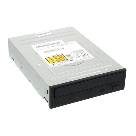
Page 33: External Part Name
External Part Name 1.Front Up/Down Volume Earphone jack Disc tray Stop/Open button Emergency HOLE 2.Rear Master/Slave select pin Power terminal Sound output terminal Interface terminal Digital output terminal (Optional) -
Page 34: Disassembly Method
Disassembly Method 1. COVER BOTTOM ASSY disassembly Remove 4 screws on the bottom of COVER BOTTOM ASSY, lift the back up and disassemble COVER BOTTOM ASSY as shown in the figure of the next page. 2. COVER-TOP disassembly After disassembling 6 hooks of FRONT ASSY from COVER TOP , pull COVER TOP forward... - Page 35 Exploded Views...
- Page 36 Device Part List PARTS SPECFICATION COUNT Code FULL DESK ASSY ASS’Y CLAMPER BG97-00013A -BRKT CLAMPER SECC 0.8T BG61-00010A -CLAMPER UPPER BG66-90013A -CLAMPER LOWER BG66-00001A -MAGNET CLAMPER Nd-Fe-B(N35H) BG33-30001D -BRKT MAGNET SECC 0.8T BG61-00018A TRAY DISC PC/ABS BG66-00002A ASS’Y LOADING BG97-00017A -MAIN FRAME BG61-00011A -MOTOR DC...
-
Page 37: Packing Options
Packing Options PARTS CODE NO. SPECIFICATION Q’ TY REMAR PACKING-CASE BG69-00017A SW-1E CUSHION-SET BG69-20327A BAG-PE BG69-30305A LDPE DISC-FLOPPY BG46-30001J 3.5 INCH CABLE-WIRE BG39-42001A HARNESS PE-BAG BG69-30307A LDPE MANUAL-USERS BG68-00043A CABLE-IF BG39-30002A 380MM... - Page 38 Electrical Parts List SC-148B MAIN PCB CODE NO LOC.NO SPEC 0801-002143 IC310 7S32 1001-001003 IC203 TC4S66F 1003-001221 IC501 M56788FP 1003-001227 IC502 TA8493AF 1005-001006 IC401 TC9474FA 1203-001500 IC602 PQ20WZ5U 1103-001144 IC304 29EE512-70 BG09-00002A IC301 KS88C4504-14 0904-001367 IC201 TC9450BF 1201-001476 IC101 TA2143FN...
- Page 39 R-CHIP CODE NO LOC.NO SPEC 2007-000034 R520,R521,R522,R523,R524 1(1/8W) R525,R535 2007-000060 R516 100K-F 2007-000070 R205,R325,R333 R280,R310,R108,R109 2007-000071 R402,R403,R406,R408,R409 R518 2007-000074 R101 2007-000077 R732 2007-000078 R316,R317,R318,R401,R135,R712 15 R117,R119,R201,R202,R326 R315,R713,R714,R320 2007-000080 R615 2007-000082 R203,R204,R207,R208,R106 3.3K 2007-000084 R311,R312,R313,R314,R335 4.7K R118 2007-000090 R432,R443,R711 R327,R433,R437,R438,R439 R440,R442,R526,R527,R717 R718 2007-000092 R301,R503...
- Page 40 OTHERS CODE NO LOC.NO SPEC 2703-000398 L101 10uH 2802-001046 X401 50MHZ 2802-001047 X201 33.8688MHZ 2802-001068 X301 20MHZ 3301-001082 B601,B602,B603,B604 BEAD 3704-000249 IC306S SOCKET-IC 3708-001346 CN702 13PIN 3708-001347 CN503 4PIN 3708-001348 CN502 11PIN 3708-001380 CN501 17PIN 3711-003262 CN701 5IN1 0407-000116 D101 DAP202K 0501-000251 Q102,Q501...
- Page 41 SC-148B FRONT PCB SPEC CODE NO LOC.NO BG41-00019A 0.2 PCB-FRONT;SC-148B,-,-,1.6T*247*162 2401-001246 C701,C702 C-AL;4.7uF,20%,25V,WT,TP,3.5x5mm,2. 2401-000249 C703,C705 C-AL;100uF,20%,10V,GP,TP,6.3x5,2.5 2401-001476 C704,C709 C-AL;47uF,20%,10V,GP,TP,6.3x5mm,2.5 2401-000213 C710,C706,C707 C-AL;100nF,20%,50V,GP,TP,3x5,2.5 BG41-00004A CN701 FPC;FFC-FRONT,0.3,13P,SD-604F 0601-001332 D701 LED;CBI,GRN,2.9mm,567nm BG14-10001N IC701 IC-H/P AMP;BH3543,SOP,8P,H/P AMP for CD-ROM 3722-001338 JK701 JACK-DC POWER;6P/3C,3.6mm,SN,BLK,NO 3301-001015...
- Page 42 Block Diagram...
- Page 43 Block Diagram...
- Page 44 Operational Position Diagram...
- Page 45 Operational Position Diagram...
- Page 46 Operational Position Diagram...
- Page 47 Operational Position Diagram...
- Page 48 Operational Position Diagram...
- Page 49 Operational Position Diagram...
- Page 50 Operational Position Diagram...
- Page 51 Operational Position Diagram...
- Page 52 Operational Position Diagram...
- Page 53 Operational Position Diagram...
-
Page 55: Circuit Diagram
Circuit Diagram...