
Related Manuals for Harman Kardon HK 990/230


Summary of Contents for Harman Kardon HK 990/230
-
Page 1: Service Manual
Service Manual HK 990/230 2 x 200W INTEGRATED STEREO AMPLIFIER Released EU2009 harman/kardon, Inc. Rev 0, 03/2009 250 Crossways Park Dr. Woodbury, New York, 11797... -
Page 3: Specifications
Depth includes Volume Button and Loudspeaker Terminals Weight 24 kg 250 Crossways Park Drive, Woodbury, New York 11797 www.harmankardon.com Harman Consumer Group International: 2, Route de Tours, 72500 Château-du-Loir, France © 2008 Harman Kardon, Incorporated Part no. 8509 9012 0000... -
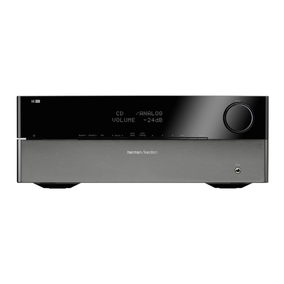
Page 4: Controls And Functions
Controls and Functions Power Indicator: This LED will illuminate Input Source Selector: Select input source Level Settings Button: Press to enter/exit in amber when the unit is in the Standby mode for listening by pressing one of the ”Source” but- the Balance left/right adjustment for the speakers to signal that the unit is ready to be turned on. - Page 5 Coil (low output and low impedance) car- CDR input jacks, for CD Recorder analog tridge. Remote OUT. Connect other Harman Kardon replay. devices (you may also experiment with other If your record player has a separate Ground...
-
Page 6: Remote Control
Remote Control Band: Switches between frequency bands on a Mute: Press this button to momentarily silence Tuner. the HK 990. “Muted” flashes in the front panel display. Press again to re-activate sound output. FM Mode: Switches between Stereo and Mono on a Tuner. - Page 7 AMP Adjustment Iding Adjustment Precaution for handling measuring instrument The ground side of the measuring instrument to be connected to the speaker terminal of this unit must be kept in floating condition because this unit is equiped with the floating balanced power amplifier.
- Page 9 High Performance Multibit - DAC with SACD Playback AD1955ARS FEATURES FUNCTIONAL BLOCK DIAGRAM 5 V Power Supply Stereo Audio DAC System Accepts 16-/18-/20-/24-Bit Data MASTER CONTROL BITSTREAM Supports 24-Bit, 192 kHz Sample Rate PCM Audio Data CLOCK INPUT DATA INPUT INPUT Supports SACD Bit Stream and External Digital Filter Interface...
- Page 10 AD1955ARS ABSOLUTE MAXIMUM RATINGS PACKAGE CHARACTERISTICS Parameter Unit Package Unit to DGND –0.3 °C/W (Thermal Resistance 109.0 to AGND –0.3 [Junction-to-Ambient]) Digital Inputs DGND – 0.3 + 0.3 °C/W (Thermal Resistance 39.0 Analog Outputs AGND – 0.3 + 0.3 [Junction-to-Case]) AGND to DGND –0.3 +0.3...
- Page 11 Advanced AMS1117 Monolithic 1A LOW DROPOUT VOLTAGE REGULATOR Systems FEATURES APPLICATIONS • • Three Terminal Adjustable or Fixed Voltages* • • High Efficiency Linear Regulators • • Post Regulators for Switching Supplies 1.5V, 1.8V, 2.5V, 2.85V, 3.3V and 5.0V • • Output Current of 1A •...
- Page 12 BSS123 N-CHANNEL ENHANCEMENT MODE FIELD EFFECT TRANSISTOR Features · Low Gate Threshold Voltage SOT-23 · Low Input Capacitance · Fast Switching Speed 0.37 0.51 · Low Input/Output Leakage 1.20 1.40 · High Drain-Source Voltage Rating 2.30 2.50 0.89 1.03 Mechanical Data TOP VIEW 0.45 0.60...
- Page 13 ICS83905 Integrated Circuit , 1:6 C RYSTAL NTERFACE Systems, Inc. LVCMOS / LVTTL F ANOUT UFFER ENERAL ESCRIPTION EATURES • 6 LVCMOS / LVTTL outputs The ICS83905 is a low skew, 1-to-6 LVCMOS / LVTTL Fanout Buffer and a member of the •...
-
Page 14: High Performance
OPA134 ® OPA2134 OPA4134 High Performance AUDIO OPERATIONAL AMPLIFIERS FEATURES DESCRIPTION ● SUPERIOR SOUND QUALITY The OPA134 series are ultra-low distortion, low noise operational amplifiers fully specified for audio appli- ● ULTRA LOW DISTORTION: 0.00008% cations. A true FET input stage was incorporated to ●... - Page 15 PCA9554A REMOTE 8-BIT I C AND SMBus I/O EXPANDER WITH INTERRUPT OUTPUT AND CONFIGURATION REGISTERS www.ti.com SCPS127A – SEPTEMBER 2006 – REVISED FEBRUARY 2007 FEATURES • I C to Parallel Port Expander • Power-Up With All Channels Configured as Inputs •...
- Page 16 Burr Brown Products from Texas Instruments SRC4392 SBFS029B – DECEMBER 2005 – REVISED APRIL 2006 Two-Channel, Asynchronous Sample Rate Converter with Integrated Digital Audio Interface Receiver and Transmitter FEATURES • Digital Audio Interface Receiver (DIR) • Two-Channel Asynchronous Sample Rate –...
- Page 17 WM8740 24-bit, High Performance 192kHz Stereo DAC Advanced Information, July 2000, Rev 1.7 DESCRIPTION FEATURES • 120dB SNR (‘A’ weighted mono @48kHz), THD+N: -104dB The WM8740 is a very high performance stereo DAC @ FS designed for audio applications such as CD, DVD, home •...
- Page 18 PIC18F66J10 FAMILY Program Memory MSSP SRAM Data CCP/ 10-bit Device Memory ECCP Flash # Single-Word Master A/D (ch) SPI™ (bytes) (PWM) (bytes) Instructions C™ PIC18F65J10 16384 2048 PIC18F65J15 24576 2048 PIC18F66J10 32768 2048 PIC18F66J15 49152 3936 PIC18F67J10 128K 65536 3936 PIC18F85J10 16384 2048...
- Page 19 NJW1159M 2-CHANNEL ELECTRONIC VOLUME ■ ■ ■ ■ GENERAL DESCRIPTION ■ ■ ■ ■ PACKAGE OUTLINE NJW1159 NJW1159M NJW1159D NJW1159V ■ ■ ■ ■ FEATURES ● ● ● ● ● ● ■ ■ ■ ■ BLOCK DIAGRAM...
-
Page 20: General Description
November 2004 LM137/LM337 3-Terminal Adjustable Negative Regulators n Excellent thermal regulation, 0.002%/W General Description n 77 dB ripple rejection The LM137/LM337 are adjustable 3-terminal negative volt- n Excellent rejection of thermal transients age regulators capable of supplying in excess of −1.5A over n 50 ppm/˚C temperature coefficient an output voltage range of −1.2V to −37V. - Page 21 August 1999 LM117/LM317A/LM317 3-Terminal Adjustable Regulator General Description age, supplies of several hundred volts can be regulated as long as the maximum input to output differential is not ex- The LM117 series of adjustable 3-terminal positive voltage ceeded, i.e., avoid short-circuiting the output. regulators is capable of supplying in excess of 1.5A over a Also, it makes an especially simple adjustable switching 1.2V to 37V output range.
-
Page 22: Thermal Data
L7805CV ABSOLUTE MAXIMUM RATINGS Symbol Parameter Value Unit DC Input Voltage (for V = 5 to 18V) (for V = 20, 24V) Output Current Internally limited Power Dissipation Internally limited Operating Junction Temperature Range (for L7800) -55 to 150 (for L7800C) 0 to 150 Storage Temperature Range -65 to 150... - Page 23 Advanced AMS1085CT Monolithic 3A LOW DROPOUT VOLTAGE REGULATOR Systems FEATURES APPLICATIONS • • Three Terminal Adjustable or Fixed Voltages • • High Efficiency Linear Regulators • • Post Regulators for Switching Supplies 1.5V, 2.5V, 2.85V, 3.0V, 3.3V, 3.5V and 5.0V •...
-
Page 24: Connection Diagram
Low Cost, General Purpose High Speed JFET Amplifier AD825 FEATURES CONNECTION DIAGRAM High Speed 8-Lead Plastic SOIC (R) Package 41 MHz, –3 dB Bandwidth 125 V/ s Slew Rate 80 ns Settling Time Input Bias Current of 20 pA and Noise Current of AD825 10 fA/√Hz –IN... - Page 25 July 2008 TIP31/TIP31A/TIP31B/TIP31C NPN Epitaxial Silicon Transistor Features • Complementary to TIP32/TIP32A/TIP32B/TIP32C 1. Base 2. Collector 3. Emitter Absolute Maximum Ratings =25 C unless otherwise noted Symbol Parameter Value Units Collector-Base Voltage : TIP31 : TIP31A : TIP31B : TIP31C Collector-Emitter Voltage : TIP31 : TIP31A : TIP31B...
- Page 26 July 2008 TIP32/TIP32A/TIP32B/TIP32C PNP Epitaxial Silicon Transistor Features • Complementary to TIP31/TIP31A/TIP31B/TIP31C 1. Base 2. Collector 3. Emitter Absolute Maximum Ratings =25 C unless otherwise noted Symbol Parameter Value Units Collector-Base Voltage : TIP32 - 40 : TIP32A - 60 : TIP32B - 80 : TIP32C...
- Page 27 ULN2001A, ULN2002A, ULN2003A, ULN2004A DARLINGTON TRANSISTOR ARRAYS SLRS027 – DECEMBER 1976 – REVISED APRIL 1993 HIGH-VOLTAGE HIGH-CURRENT DARLINGTON TRANSISTOR ARRAYS 500-mA Rated Collector Current D OR N PACKAGE (Single Output) (TOP VIEW) High-Voltage Outputs . . . 50 V Output Clamp Diodes Inputs Compatible With Various Types of Logic Relay Driver Applications...
-
Page 29: Srs® Circle Surround™ Ii (Cs Ii)
Aureus TMS320DA708, TMS320DA708B, TMS320DA788B Floating-Point Digital Signal Processors www.ti.com SPRS297E – JULY 2005 – REVISED JULY 2007 1 Second Generation Aureus™ DSPs 1.1 Features • DA708/B/DA788B: 32-/64-Bit 250-/266-MHz Floating-Point DSP • Upgrades to C67x+ CPU From DA6xx Family: – 2X CPU Registers [64 General-Purpose] –... - Page 30 Aureus TMS320DA708, TMS320DA708B, TMS320DA788B Floating-Point Digital Signal Processors www.ti.com SPRS297E – JULY 2005 – REVISED JULY 2007 1.2 Trademarks Aureus, Perfect Playback, DSP/BIOS, PowerPAD, TMS320C6000, C6000, Code Composer Studio, XDS, TMS320, TMS320C62x, and TMS320C67x are trademarks of Texas Instruments. Audyssey MultEQ XT, MultEQ, PrevEQ, and 2EQ are registered trademarks of Audyssey Laboratories. SRS is a registered trademark of SRS Labs, Inc.
- Page 31 Aureus TMS320DA708, TMS320DA708B, TMS320DA788B Floating-Point Digital Signal Processors www.ti.com SPRS297E – JULY 2005 – REVISED JULY 2007 2.13 Pin Maps Figure 2-2 shows the pin assignments on the 144-pin RFP package. Figure 2-2. 144-Pin Low-Profile Quad Flatpack (RFP Suffix)—Top View Device Overview Submit Documentation Feedback...
- Page 32 Aureus TMS320DA708, TMS320DA708B, TMS320DA788B Floating-Point Digital Signal Processors www.ti.com SPRS297E – JULY 2005 – REVISED JULY 2007 PowerPAD™ Plastic Quad Flatpack Mechanical Data Drawing (RFP) DA708/B/DA788B Device-Specific RFP (S-PQFP-G144) PowerPAD™ PLASTIC QUAD FLATPACK 0 ° − ° All linear dimensions are in millimeters. This drawing is subject to change without notice.
-
Page 33: Document Title
64Mb Synchronous DRAM based on 1M x 4Bank x16 I/O Document Title 4Bank x 1M x 16bits Synchronous DRAM Revision History Revision No. History Draft Date Remark First Version Release Nov. 2004 1. Changed tOH: 2.0 --> 2.5 [tCK = 7 & 7.5 (CL3) Product] 1. -
Page 34: Ordering Information
Synchronous DRAM Memory 64Mbit (4Mx16bit) HY57V641620E(L/S)T(P)-xI Series DESCRIPTION The Hynix HY57V641620E(L/S)T(P) series is a 67,108,864bit CMOS Synchronous DRAM, ideally suited for the memory applications which require wide data I/O and high bandwidth. HY57V641620E(L/S)T(P) is organized as 4banks of 1,048,576x16. HY57V641620E(L/S)T(P) is offering fully synchronous operation referenced to a positive edge of the clock. All inputs and outputs are synchronized with the rising edge of the clock input. -
Page 35: Pin Assignments
Synchronous DRAM Memory 64Mbit (4Mx16bit) HY57V641620E(L/S)T(P)-xI Series PIN ASSIGNMENTS DQ15 VDDQ VSSQ DQ14 DQ13 VSSQ VDDQ DQ12 DQ11 VDDQ VSSQ DQ10 54 Pin TSOPII VSSQ VDDQ 400mil x 875mil 0.8mm pin pitch LDQM UDQM /CAS /RAS A10/AP Rev. 1.5 / Feb. 2005... - Page 36 Synchronous DRAM Memory 64Mbit (4Mx16bit) HY57V641620E(L/S)T(P)-xI Series PIN DESCRIPTION SYMBOL TYPE DESCRIPTION The system clock input. All other inputs are registered to the Clock SDRAM on the rising edge of CLK Controls internal clock signal and when deactivated, the SDRAM will Clock Enable be one of the states among power down, suspend or self refresh Chip Select...
-
Page 37: Functional Block Diagram
Synchronous DRAM Memory 64Mbit (4Mx16bit) HY57V641620E(L/S)T(P)-xI Series FUNCTIONAL BLOCK DIAGRAM 1Mbit x 4banks x 16 I/O Synchronous DRAM Internal Row Self refresh Counter logic & timer 1Mx16 BANK 3 1Mx16 BANK 2 Row Active 1Mx16 BANK 1 Decoder 1Mx16 BANK 0 Refresh Memory Cell... -
Page 38: Distinctive Characteristics
S29AL016D 16 Megabit (2 M x 8-Bit/1 M x 16-Bit) CMOS 3.0 Volt-only Boot Sector Flash Memory Data Sheet PRELIMINARY Distinctive Characteristics Architectural Advantages Ultra low power consumption (typical values at 5 MHz) Single power supply operation — 200 nA Automatic Sleep mode current —... -
Page 39: Connection Diagrams
P r e l i m i n a r y Connection Diagrams BYTE# DQ15/A-1 DQ14 DQ13 DQ12 RESET# Standard TSOP DQ11 RY/BY# DQ10 RESET# Standard SOP BYTE# DQ15/A-1 DQ14 DQ13 DQ10 DQ12 DQ11 S29AL016D S29AL016D_00_A2 December 17, 2004... -
Page 40: Special Handling Instructions
P r e l i m i n a r y Connection Diagrams FBGA Top View, Balls Facing Down BYTE# DQ15/A-1 DQ14 DQ13 RESET# DQ12 RY/BY# DQ10 DQ11 Special Handling Instructions Special handling is required for Flash Memory products in FBGA packages. Flash memory devices in FBGA packages may be damaged if exposed to ultra- sonic cleaning methods. -
Page 41: Pin Configuration
P r e l i m i n a r y Pin Configuration A0–A19 20 addresses DQ0–DQ14 15 data inputs/outputs DQ15/A-1 DQ15 (data input/output, word mode), A-1 (LSB address input, byte mode) BYTE# Selects 8-bit or 16-bit mode Chip enable Output enable Write enable RESET#... -
Page 42: Physical Dimensions
P r e l i m i n a r y Physical Dimensions TS 048—48-Pin Standard TSOP S29AL016D S29AL016D_00_A2 December 17, 2004... - Page 43 P r e l i m i n a r y 0.10 STANDARD PIN OUT (TOP VIEW) 2X (N/2 TIPS) 0.10 0.10 REVERSE PIN OUT (TOP VIEW) SEE DETAIL B 0.25 SEATING 2X (N/2 TIPS) PLANE SEE DETAIL A 0.08MM (0.0031") C A - B S WITH PLATING...
- Page 44 SN74LVC823A 9-BIT BUS-INTERFACE FLIP-FLOP WITH 3-STATE OUTPUTS www.ti.com SCAS305I – MARCH 1993 – REVISED FEBRUARY 2005 FEATURES • Operates From 1.65 V to 3.6 V ( T O • Inputs Accept Voltages to 5.5 V • Max t of 7.9 ns at 3.3 V •...
-
Page 45: Function Table
SN74LVC823A 9-BIT BUS-INTERFACE FLIP-FLOP WITH 3-STATE OUTPUTS www.ti.com SCAS305I – MARCH 1993 – REVISED FEBRUARY 2005 DESCRIPTION/ORDERING INFORMATION (CONTINUED) A buffered output-enable (OE) input can be used to place the nine outputs in either a normal logic state (high or low logic levels) or the high-impedance state. -
Page 46: Pin Assignment
DS1818 3.3V EconoReset with Pushbutton www.maxim-ic.com FEATURES PIN ASSIGNMENT § Automatically restarts a microprocessor after power failure DALLAS § Monitors pushbutton for external override DS1818 Econo § Maintains reset for 150 ms after V Reset returns to an in-tolerance condition §... -
Page 47: General Description
March 1999 Revised February 2005 NC7WZ07 TinyLogic£ UHS Dual Buffer (Open Drain Outputs) General Description Features ■ Space saving SC70 6-lead package The NC7WZ07 is a dual buffer with open drain outputs £ ¥ from Fairchild's Ultra High Speed Series of TinyLogic ■... - Page 48 Logic Symbol Connection Diagrams IEEE/IEC Pin Assignments for SC70 (Top View) Pin Descriptions Pin One Orientation Diagram Pin Names Description Data Inputs Output Function Table AAA represents Product Code Top Mark - see ordering code Note: Orientation of Top Mark determines Pin One location. Read the top product code mark left to right, Pin One is the lower left pin (see diagram).
-
Page 49: Typical Application
www.fairchildsemi.com FAN1112 1A 1.2V Low Dropout Linear Regulator Features Description • Low dropout voltage The FAN1112 is a 1.2V low dropout three-terminal • Load regulation: 0.05% typical regulator with 1A output current capability. The device has • Trimmed current limit been optimized for low voltage where transient response and •... -
Page 50: Product Specification
PRODUCT SPECIFICATION FAN1112 Pin Assignments Front View Tab is V Front View Tab is GND OUT 4-Lead Plastic SOT-223 3-Lead Plastic TO-252 Θ Θ = 15°C/W* = 3°C/W* *With package soldered to 0.5 square inch copper area over backside ground plane or internal power plane., Θ can vary from 30°C/W to more than 50°C/W. -
Page 51: Data Sheet
PIC18F87J10 Family Data Sheet 64/80-Pin High-Performance, 1-Mbit Flash Microcontrollers with nanoWatt Technology Advance Information 2005 Microchip Technology Inc. DS39663A... - Page 52 Note the following details of the code protection feature on Microchip devices: • Microchip products meet the specification contained in their particular Microchip Data Sheet. • Microchip believes that its family of products is one of the most secure families of its kind on the market today, when used in the intended manner and under normal conditions.
- Page 53 PIC18F87J10 FAMILY 64/80-Pin, High-Performance, 1-Mbit Flash Microcontrollers with nanoWatt Technology Special Microcontroller Features: Peripheral Highlights: • Operating voltage range: 2.0V to 3.6V • High-current sink/source 25 mA/25 mA (PORTB and PORTC) • 5.5V tolerant input (digital pins only) • Four programmable external interrupts •...
- Page 54 PIC18F87J10 FAMILY Program Memory MSSP SRAM Data CCP/ 10-bit Device Memory ECCP Flash # Single-Word Master A/D (ch) SPI™ (bytes) (PWM) (bytes) Instructions C™ PIC18F65J10 16384 2048 PIC18F65J15 24576 2048 PIC18F66J10 32768 2048 PIC18F66J15 49152 3936 PIC18F67J10 128K 65536 3936 PIC18F85J10 16384 2048...
-
Page 55: Serial Eeprom
Features • Low-voltage and Standard-voltage Operation – 2.7 (V = 2.7V to 5.5V) – 1.8 (V = 1.8V to 5.5V) • Internally Organized 128 x 8 (1K), 256 x 8 (2K), 512 x 8 (4K), 1024 x 8 (8K) or 2048 x 8 (16K) •... -
Page 56: Block Diagram
LD1117 SERIES LOW DROP FIXED AND ADJUSTABLE POSITIVE VOLTAGE REGULATORS LOW DROPOUT VOLTAGE (1V TYP) ■ 2.85V DEVICE PERFORMANCES ARE ■ SUITABLE FOR SCSI-2 ACTIVE TERMINATION OUTPUT CURRENT UP TO 800mA ■ SOT-223 SO-8 FIXED OUTPUT VOLTAGE OF: 1.8V, 2.5V, ■... -
Page 57: Application Circuit
LD1117 SERIES ABSOLUTE MAXIMUM RATINGS Symbol Parameter Value Unit DC Input Voltage Power Dissipation to t Storage Temperature Range -40 to 150 Operating Junction Temperature Range 0 to 125 Absolute Maximum Ratings are those value beyond which damage to the device may occur. Functional operation under these condition is not implied. - Page 58 LD1117 SERIES CONNECTION DIAGRAM AND ORDERING NUMBERS (top view) SOT-223 SO-8 DPAK TO-220 SOT-223 SO-8 DPAK TO-220 Output Voltage LD1117S18 LD1117D18 LD1117DT18 LD1117V18 1.8V LD1117S18C LD1117D18C LD1117DT18C LD1117V18C 1.8V LD1117S25 LD1117D25 LD1117DT25 LD1117V25 2.5V LD1117S25C LD1117D25C LD1117DT25C LD1117V25C 2.5V LD1117S28 LD1117D28 LD1117DT28 LD1117V28...
- Page 59 www.fairchildsemi.com KA78XX/KA78XXA 3-Terminal 1A Positive Voltage Regulator Features Description • Output Current up to 1A The KA78XX/KA78XXA series of three-terminal positive • Output Voltages of 5, 6, 8, 9, 10, 12, 15, 18, 24V regulator are available in the TO-220/D-PAK package and •...
- Page 61 19-4323; Rev 10; 8/01 +5V-Powered, Multichannel RS-232 Drivers/Receivers General Description ____________________________Features The MAX220–MAX249 family of line drivers/receivers is Superior to Bipolar intended for all EIA/TIA-232E and V.28/V.24 communica- ♦ Operate from Single +5V Power Supply tions interfaces, particularly applications where ±12V is (+5V and +12V—MAX231/MAX239) not available.
- Page 62 +5V-Powered, Multichannel RS-232 Drivers/Receivers +5V INPUT TOP VIEW 2 +10V +5V TO +10V VOLTAGE DOUBLER -10V +10V TO -10V VOLTAGE INVERTER MAX220 MAX232 400k MAX232A TTL/CMOS RS-232 INPUTS 400k OUTPUTS DIP/SO R1 I TTL/CMOS RS-232 CAPACITANCE (µF) OUTPUTS INPUTS DEVICE MAX220 MAX232 MAX232A...
- Page 63 2SC2073 2SC2406 1. BASE 2. COLLECTOR 3. EMITTER 2SC1815 2SA950 2SC2458 2SC2235 2SC2120 1. EMITTER 1. EMITTER 1. EMITTER 1. EMITTER 1. EMITTER 2. COLLECTOR 2. COLLECTOR 2. COLLECTOR 2. COLLECTOR 2. COLLECTOR 3. BASE 3. BASE 3. BASE 3. BASE 3.
- Page 64 Low Cost, General-Purpose High Speed JFET Amplifier AD825 FEATURES CONNECTION DIAGRAMS High speed 41 MHz, −3 dB bandwidth AD825 –IN 125 V/µs slew rate TOP VIEW OUTPUT (Not to Scale) 80 ns settling time –V Input bias current of 20 pA and noise current of 10 fA/√Hz NC = NO CONNECT Input voltage noise of 12 nV/√Hz Figure 1.
- Page 65 ASAHI KASEI [AK4683] AK4683 Asynchronous Multi-Channel Audio CODEC with DIR/T GENERAL DESCRIPTION The AK4683 is a single chip CODEC that includes two channels of ADC and four channels of DAC. The ADC outputs 24bit data and the DAC accepts up to 24bit input data. The ADC has the Enhanced Dual Bit architecture with wide dynamic range.
-
Page 66: Top View
ASAHI KASEI [AK4683] Ordering Guide AK4683EQ -20 +85 C 64pin LQFP (0.5mm pitch) AKD4683 Evaluation Board for AK4683 Pin Layout 64 63 62 61 60 59 58 57 56 55 54 53 52 51 50 49 PVDD RISEL ROPIN LOPIN LISEL AVSS2 AVDD2... - Page 67 ASAHI KASEI [AK4683] PIN/FUNCTION Pin Name Function PVDD PLL Power supply Pin, 4.5V 5.5V Receiver Channel 0 Pin (Internal biased pin. Internally biased at PVDD/2) Control Mode Select Pin. “L”: 4-wire Serial, “H”: I C Bus Receiver Channel 1 Pin Receiver Channel 2 Pin Receiver Channel 3 Pin Interrupt Pin...
- Page 68 ASAHI KASEI [AK4683] Pin Name Function LOUT2 DAC2 Lch Positive Analog Output Pin ROUT2 DAC2 Rch Positive Analog Output Pin LOUT1 DAC1 Lch Positive Analog Output Pin ROUT1 DAC1 Rch Positive Analog Output Pin DAC/ADC Common Voltage Output Pin VCOM 2.2 F capacitor should be connected to AVSS2 externally.
- Page 69 CS5361 114 dB, 192 kHz, Multi-Bit Audio A/D Converter Features General Description The CS5361 is a complete analog-to-digital converter for Advanced Multi-bit Delta-sigma Architecture digital audio systems. It performs sampling, analog-to- 24-bit Conversion digital conversion, and anti-alias filtering. The CS5361 generates 24-bit values for both left and right inputs in 114 dB Dynamic Range serial form at sample rates up to 192 kHz per channel.
-
Page 70: Pin Descriptions
CS5361 2.0 PIN DESCRIPTIONS FILT+ REFGND LRCK SCLK AINR+ MCLK AINR- AINL- SDOUT AINL+ MDIV OVFL S/LJ Pin Name Pin Description Reset (Input) - The device enters a low power mode when low. Master/Slave Mode (Input) - Selects operation as either clock master or slave. Left Right Clock (Input/Output) - Determines which channel, Left or Right, is currently active on the LRCK serial audio data line. - Page 75 Philips Semiconductors Product data sheet 16-bit I C and SMBus I/O port with interrupt PCA9555 DESCRIPTION The PCA9555 is a 24-pin CMOS device that provide 16 bits of General Purpose parallel Input/Output (GPIO) expansion for C/SMBus applications and was developed to enhance the Philips family of I@C I/O expanders.
- Page 76 Philips Semiconductors Product data sheet 16-bit I C and SMBus I/O port with interrupt PCA9555 PIN CONFIGURATION — DIP, SO, SSOP, TSSOP PIN CONFIGURATION — HVQFN I/O0.0 I/O1.7 I/O0.1 I/O0.0 I/O1.6 I/O0.2 I/O0.1 I/O1.7 I/O0.3 I/O1.5 I/O0.2 I/O1.6 I/O0.3 I/O1.5 I/O0.4 I/O1.4 I/O0.4...
- Page 77 Philips Semiconductors Product data sheet 16-bit I C and SMBus I/O port with interrupt PCA9555 BLOCK DIAGRAM PCA9555 I/O1.0 I/O1.1 I/O1.2 INPUT/ I/O1.3 8-BIT OUTPUT PORTS I/O1.4 I/O1.5 WRITE pulse I/O1.6 READ pulse I/O1.7 C/SMBUS CONTROL I/O0.0 I/O0.1 I/O0.2 INPUT INPUT/ 8-BIT I/O0.3...
- Page 79 TL071, TL071A, TL071B, TL072 TL072A, TL072B, TL074, TL074A, TL074B LOW-NOISE JFET-INPUT OPERATIONAL AMPLIFIERS SLOS080D – SEPTEMBER 1978 – REVISED AUGUST 1996 Low Power Consumption Low Noise = 18 nV/√Hz Typ at f = 1 kHz Wide Common-Mode and Differential Voltage Ranges High Input Impedance .
- Page 80 TL071, TL071A, TL071B, TL072 TL072A, TL072B, TL074, TL074A, TL074B LOW-NOISE JFET-INPUT OPERATIONAL AMPLIFIERS SLOS080D – SEPTEMBER 1978 – REVISED AUGUST 1996 TL071, TL071A, TL071B TL072, TL072A, TL072B TL074, TL074A, TL074B D, JG, P, OR PW PACKAGE D, JG, P, OR PW PACKAGE D, J, N, OR PW PACKAGE (TOP VIEW) (TOP VIEW)
- Page 81 2SA1298 PNP 3-Pin Regulaeor IC 2SA1312 PNP LD1117S5.0 DTC343TK NPN 2SC3324 NPN 2SC3265 NPN 2SC1035 NPN V OUT V IN 1) Emitter SOT-223 2) Base 3) Collector...
- Page 102 DSP & Oscillator DSP & Oscillator WM_BITCLK SDATAR1 WM_SDATA WM_LRCLK WDCLK I2C_SCL SDATAL2 SDATAL1 SDATAR2 SRC_SDATA BITCLK SRC_BITCLK Digital Inputs SRC_LRCLK Digital Inputs SDATAR2 I2C_SDA Subwoofer DAC WDCLK SRC_INT# DAC_L Subwoofer DAC CS_AD1955_2# CLK_24_MHZ_4 SRC_AESOUT RST_SRC# ADC_LRCLK CLK_24_MHZ_2 I2C_SCL ADC_BITCLK BITCLK SRC_SDATA CS_WM8740#...
- Page 105 +3.3V FB0805 100nF C111 FB10 +3.3V FB0805 47uF/25V 150R +3.3V 100nF HR610675(Hanrun) HRS-Link +3.3V 47uF/25V +1.8V 100nF RJ45 10P8C FB0805 FB0805 300R 100nF 100nF 100nF SRC4392 is MASTERon both PORTA andPORTB 100nF SRC4392IPFBT GPO5 CLK_24_MHZ_5 74LCX125MTC RST_SRC# RESET AES_OUT RX1+ RX1- 74LCX125MTC TOSLINK...
- Page 106 +5VA +15VA +5VA 100R FB0805 100nF +5VA 47uF/16V 100nF +5VA +3.3V 74HC4052D NJM2068M C119 47uF/25V 47uF/25V 470R Subwoofer OUT L FB0805 47uF/25V 100nF C108 4.7K 100nF 2A332J DTC343TK 330pF 47uF/25V -15VA 100nF 2A332J 100nF 100R C107 SUB_MUTE_OUT 47uF/16V 100nF 47uF/25V XWM8740EDS G = 4 RST_SUB#...
- Page 107 -15V -15V IC4B TPA6120A2 IC4A TPA6120A2 +15V CK-6.35-02 L IN +15V TO Pamp PCB C2120 R IN CN13 HP DETECT 331P IN4148 HP L 331P HP R OPEN 4P(2.0) +15V RELAY1 JRC-27F/012-M(555) 2.12V +15V TO Pamp PCB 2.2K +15V -15V 150P 10u16 CN12...
- Page 108 +80V +16V 2K4 2W MJD243 Faston 6.3 60VAC diodes mounted on heatsink 230V +/- 16VDC rails current: 1. 0.2mA for TL061 +60V 0.22R(RF) 2W 2. 4mA for OPA2134 Faston 6.3 MUR2020 MUR2020 3. 4mA for input stage 45VAC + C12 22K 3W 10nF/250V 10nF/250V...
- Page 109 +80V + C18 150R 3W 150R 1/4W 1% 220uF/100V 47nF/100V +16V +16V DL4148 47nF/100V +16V +60V BAS20 BDS-3S5 2SC3324 DL4148 2SA1312 2SC3324 2SC3324 MJD253 MJL3281A MJL3281A NJL3281D MJL3281A MJL3281A DL4148 2SC4793 2SA1312 DL4148 180R 2SC4935 2SC3324 2SC3324 2SA1837 MJE15032 DL4148 BAS20 270R 330R...
- Page 110 100R CS_VOL# Volume AV2-8.4-14/EC R100 100R PREOUT_L 100R 100R OUTL R105 100K 2.2nF R109 OPEN LATCH BOUTL 100PF 100PF 100PF PREOUT_R CLOCK VDD_OUT Interface 10uF/50V & R110 +15VA DATA BOUTR Logic R107 100K ANALOG_IN_L OPEN 47uF/16V 100nF 100R OUTR 100R JRC-27F/005-M(555) 100nF VSS_OUT...
- Page 111 PHONO DIGITAL I/O ANALOG I/O SRC_AESOUT CLK_24MHZ CLK_24MHZ BITCLK_ADC LRCLK_ADC 2*4P2.0(180) 2*4P2.0(180) SDATA_ADC SPDIF_REC INT_AK4683_5V 2SC2406 INT_AK4683 +3.3V MUTE_OUT CDR_SEL DAC_L DAC_R ANALOG_IN_L ANALOG_IN_R TAPE_SEL CDR_SEL 2SC2406 NJU7313_SCK MUTE_LISTEN# REC OUT_L REC OUT_R REC OUT_L REC OUT_R SUB_MUTE_OUT +3.3V IN_L IN_R CS_AD1955_1# CS_AD1955_2#...
- Page 112 +3.3V +3.3V MC_MM# BAS16 Barrette 6P ULN2003AD +3.3V +3.3V RL_MIC JRC-27F/005-M(555) +3.3V +5VSTBY 470R 10uF/50V PREOUT_RELAY FB0805 FB0805 JRC-27F/005-M(555) 47uF/25V 47uF/25V JRC-27F/005-M(555) 2SC2406 RL_DIRECT 100nF +3.3V +3.3V R103 HEADPHONE_MICRO# 2SC2406 100nF TO IR PCB 10uF/50V 100nF PIC18F66J10 +3.3V MCLR R106 RA0/AN0 RD0/PSP0 CS_AD1955_1#...
- Page 113 VOUT 100nF 220uF/10V 100nF L7805CV Chassis screwed transformer GBU806 AMS1085CT +3.3V +11v 1.5A 100nF 230V 4.7mF/16V 4.7mF/16V 412R/1% 220uF/10V 100nF 680R/1% 10UF/50V RF0.22R/0.5W RF0.22R/0.5W 15.5V 0.5A 5P2.5 30BQ040PbF +VCC GBU806 +15VA 15.5V TO FUSE BOARD TIP31C +20VA 0.5A VOUT 100R 100nF 220R 10uF/50V...
- Page 114 16-BT-151GINK +3.3V 2SC2406 DGND 100U16(NC) 16-BT-151GINK 104(NC) 2SC2406 MAX3232CDR(NC) DGND DGND 4.7K R1 UOT R1 IN CN14 T1 IN T1 OUT +3.3V 104(NC) 100R 100R DGND +3.3V 2SC2406 C1815 DGND +3.3V C1815 104(NC) 104(NC) AT24C02 DGND RESET DGND DGND DGND 6P(2.5) 4.7K 4.7K...
- Page 115 DSP_3.3V DSP_3.3V 2.2K 10/6.3 0.1UF DSP_3.3V EM_A0 EXTA12 EM_A1 EXTA13 EM_A2 EXTA14 EM_A3 EXTA15 EM_A4 EXTA16 EM_A5 EXTA17 DS1818 EM_A6 EXTA18 EM_A7 EXTA19 DSP_1.2V DSP_3.3V EM_A8 RESET_N_DSP EXTAEN CLKEN EM_CS2_N DSP_3.3V RESET_N_DSP SPI0_CLK/I2C0_SCL AHCLKX0/AHCLKX2 SPI0_SCS/I2C1_SCL VCCGND EXTAEN AMUTE0 AMUTE1 AMUTE1 SPI0_ENA/I2C1_SDA EM_OE_N 0.1UF...
- Page 116 TO Preamp CN15 1N4148 1N4148 3P(2.0) T1out R1in CKX3.5-12A 3.5mm R1out T1in T2in T2out R2out R2in IR OUT 100U10V TO MCU BOARD 47U10V CN12 10uH MCU+5V REMOTE REMOTE 10uH DGND 10uH A1015 DB-09 5P(2.0) MCU2 MCU1 A1015 SK-22H03G6-RS IR IN/OUT BOARD CKX3.5-12A 3.5mm LTV817A IR IN...
- Page 117 2.2/0.5W CN16 CN17 R73 1.2K R78 1.2K C1815 2P(2.5) 2P(2.5) CN18 A9225M12S CN19 A9225M12S 2P(2.5) 2P(2.5) DC12 0.24A C1815 DC12 0.24A TO TEMP SENSOR TO TEMP SENSOR 2SC2073 2SC2073 KA7805 A950 R82 22K FAGND FAGND JY103M(X1/400V.Y2/300V) 10/16 47/50 4.7K RAY1 100R1/4W LED+5V C2458...
- Page 118 R1.5(white)H5mm R1.5(white)H5mm R1.5(white)H5mm R1.5(white)H5mm R122ECA-D1-19.5F-24-W...
- Page 119 +15VA ANALOG IN_L P[2] R137 100R +15VA R139 100R C111 220R 100R C109 100nF 47uF16V 47uF16V AD825AR R109 100nF AV4-8.4-13/EC JRC-27F1005-M-555 100R 100R AD825AR 330P IN_L ANALOG IN_R P[2] P[2,3] R110 220K 220K -15VA -15VA JRC-27F1005-M-555 220pFM R107 100R 220pFM R111 R138 R140...
- Page 120 BAS16 JRC-27F1005-M-555 RL_PROCESSOR BAS16 2x4P2.0(90) JRC-27F1005-M-555 RL_CD P[3] SPDIF_RECORD SRC_AESOUT P[3] BAS16 JRC-27F1005-M-555 RL_TUNER CLK_24MHZ BITCLK_ADC P[1] P[1,3] SDATA_ADC LRCLK_ADC P[1] P[1] BAS16 JRC-27F1005-M-555 RL_CDR BAS16 JRC-27F1005-M-555 RL_TAPE FB-0805 BAS16 C121 JRC-27F1005-M-555 100nF RL_AUX CDR_OUT SEL 47uF/16V BAS16 2x13P2.0(90) JRC-27F1005-M-555 RL_TV PCA9555 BAS16...
- Page 121 5.1R FB-0805 -15VA A+5V 10uF/50V R142 47uF/25V 100R C113 100nF 47uF16V 100nF 100nF NJM2068 47uF16V 1.78K1% 7.5K1% 2.2uF 18K1% 680R LISEL VCOM LOPIN REC_out_R P[2] 47uF16V LOUT1 L_IN1 P[4] L_IN1 LIN1 ROUT1 LIN2 102(NPO) LIN3 LOUT2 100pF(NPO) LIN4 ROUT2 LIN5 C122 9.1K1% LIN6...
- Page 122 NJU7313AM P[1] P[1] CD_in_L CD_in_R -15VA Tuner_in_L Tuner_in_R P[1] P[1] C114 R144 47uF16V 100R P[1] Aux_in_L Aux_in_R P[1] 100nF P[1] CDR_in_L CDR_in_R P[1] P[1] Tape_in_L Tape_in_R R_IN1 P[3] P[1] 47K1% Level Shifter Level Shifter Latch Circuit Latch Circuit 10uF/50V NJM2068 P[1] TV_in_L TV_in_R...
- Page 123 +15V IN_MM_L 220uF/16V +12VAL 220uF/16V 4K7 1% 560R1% R107 R106 R119 2.7K1% 2.7K1% 470R1% 10pF 10uF/50V 2SC3324 2SC3324 2SC3324 R121 2SC3324 470K 2SA1312 R120 10R1% 120R1% 2SC3324 330R1% 330R1% R129 N1210X226KCTx5R+-5% 2SA1312 (NPO) 22R1% 7.5K1% JRC-27F1005-M-555 22uF/ELCO 10nF LED rouge 10uF16V R109 10R1%...
- Page 124 AV4-8.4-13/EC IN_MM_L +15V 100nF 220uF/16V +12VAR 220uF/16V 4K7 1% R101 R100 R113 560R1% 2.7K1% 2.7K1% 10pF 470R1% 10uF/50V 2SC3324 2SC3324 2SC3324 R115 2SC3324 470K 2SA1312 R114 10R1% 120R1% 2SC3324 330R1% 330R1% N1210X226KCTx5R+-5% R125 2SA1312 22R1% 7.5K1% IN_MC_L JRC-27F1005-M-555 R108 22uF/ELCO 6.8K1% LED rouge 10nF...
- Page 125 100nF 4.7K AV4-8.4-13/EC PHONO_IN_L DTC343TK 330pF CDR OUT PHONO_IN_R 100nF 100nF +15V -15V 4P(2.0) DTC343TK 330pF 47uF16V 47uF16V 24P (12 x 2 x 2mm)90 TAPE_SEL CDR_SEL 4.7K REC_out_L REC_out_R DTC343TK 330pF 100nF TAPE OUT DTC343TK 330pF +18VA -18VA AV4-8.4-13/EC NJU201AM JRC-27F1005-M-555 PHONO MM/MC AV-8.4-8/ES...
- Page 126 100R 100nF 47uF16V 100nF LX-1604HP-3 NJM5532M 100R 330P 100nF 47uF16V 330P NJM5532M 100R LIN+ 100nF LIN- 47uF16V RIN+ RIN- +15VA 100nF LX-1604HP-3 +15VA NJM5532M -15VA -15VA 9P(2.0) 330P 100R 100nF 47uF16V 330P NJM5532M...
- Page 129 Digital BOARD PART LIST P/N:0099-1160-0000 Used Part Type Designator Description Part number =================================== ===================== ========== 4.7pF/50V±5% X7R 0805 MLCC 2103 5479 0140 10pF/50V±5% X7R 0805 MLCC C53 C54 2103 5100 0140 10uF/25V±10% Y5V 0805 MLCC C1 C35 C66 C86 2103 5106 0140 220pF/50V±5% NPO 0805 MLCC C76 C93 2103 5221 0140...
- Page 130 74HC4052D S016 PHILIPS U6 U7 1004 0520 4913 74LCX125MTC TSSOP14 ST U4 U5 1074 1250 1915 74LCX139TTR TSSOP16 1074 1392 0815 AD1955ARS SSOP28 (Analog Device) U19 U23 1001 9550 0414 AMS1117-1.8 SOT-223 AMS 1011 7180 0156 AMS1117-3.3 SOT-223 AMS 1011 7330 0128 AMS1117-5.0 SOT-223 AMS 1011 7500 0128 0R±5% 0805...
- Page 131 IN4148 1311 1414 8000 NJM2068M SOIC8 JRC 1031 2068 1300 TPA6120A2 DWP-20 (Texas lnstrument) 1061 2020 6138 1.65K±1% 0603 2403 1216 5203 1K±5% 0603 R7 R8 R9 R10 R11 R12 R13 R14 2401 1221 0203 R25 R26 2.2K±5% 0603 2401 1222 2203 10K±5% 0603 R4 R18 R23 R24 2401 1221 0303...
- Page 132 1191 3020 1210 NJL1302D Q6 Q11 1111 8370 0130 2SA1837 1181 5033 1220 MJE15033 1111 8690 0100 2SA1869 Q9 Q18 1134 7930 0000 2SC4793 1134 9350 0120 2SC4935 Q12 Q13 Q15 Q16 1183 2810 1200 MJL3281A 1193 2810 1210 NJL3281D 1181 5032 1220 MJE15032 Q20 Q38...
- Page 133 R65 R56 2402 0912 7105 270R/1206 R67 R80 R81 2402 0913 9105 390R/1206 2402 0918 2005 82R/1206 2402 0916 8305 68K/1206 R91 R92 R93 2402 0913 3305 33K/1206 R96 R97 2413 0622 4213 2K4 /2W U2 U1 1000 8170 5501 PC817A 1002 1340 0738 OPA2134UA...
- Page 134 2SC2406R (SC-59 Panasonic) Q1 Q3 Q4 Q5 Q6 Q12 Q13 Q14 Q15 Q17 1132 4060 5000 BSS123 SOT23 Q10 Q20 1180 1230 1011 1.3K±5% 0805 R5 R7 2401 8221 3204 1K±5% 0805 R19 R20 R38 R50 R51 R59 2401 8210 2400 RF0.22R/0.5W±5% R40 R41 R42 2406 0422 2815...
- Page 135 47uF/10V±20% E.CAP C14 C17 2340 0210 0015 100uF/16V±20% E.CAP C12 C37 2311 0310 1015 7P PLUG TO HOUSING2468#26X7C 2.0 L=300MM 3307 0704 0335 4P HOUSING TO HOUSING2468#26X4C 2.0 L=60MM CN4 3304 0504 0064 5P PLUG TO HOUSING2468#26X7C 2.0 L=300MM CN13 3304 0505 0302 6P PLUG TO PHOUSING 2468#26X6C 2.0 L=380MM 3306 0504 0385...
- Page 136 2*16P(2.54)(180°) J1 J2 3113 0516 6872 2*7P(2.54)(180°) 3102 1007 5802 FB---0805 L1 L3 1852 0120 9100 2.2K---0603 2401 1222 2203 33 ---0603 R2 R3 R4 R5 R6 R7 R8 R9 R10 R11 R12 R13 R14 2401 1223 3003 R15 R16 R17 R18 R19 R20 R21 R22 R23 R29 R30 R31 R32 R33 R34 R35 R36 R37 3.3K±5% 0603 R24 R25 R26 R27 R28 R44...
- Page 137 470uF/25V±20% E.CAP 2341 0410 1015 0.1uF/50V±10% C21 C22 C44 C46 C52 2115 6104 0123 47uF/50V±20% E.CAP 2340 0610 1010 100uF/50V±20% E.CAP 2311 0610 1015 100uF/63V±20% E.CAP C28 C45 2311 0710 1015 0.1uF/275VAC(X2) 2210 3104 0600 JY103M(X1/400V.Y2/300V) 2210 3103 0600 2P(2.5) SOCKET CN16 CN17 CN18 CN19 3100 5020 0200 3P(3.96) SOCKET...
- Page 138 220 1/8W±5% R17 R18 R63 R64 2401 0222 2111 R122ECA-D1-19.5F-24-W 4401 2211 9524 HK990 PART LIST Analog I/O-PCB P/N:0099-1510-0000 Used Part Type Designator Description Part number =================================== ===================== ========== 47uF/16V--DIP C24 C26 C27 C38 C53 C108 C109 C110 C111 C1122340 0310 1015 C113 C114 C115 C116 C117 C4 C11 C41 C44 C45 C100 C120 C121 100uF/16V--DIP...
- Page 139 JRC-27F1005-M-555 K1 K2 K3 K4 K5 K6 K7 K8 K9 4712 2027 0006 FB--L_0805 L2 L3 L5 L6 L7 1852 0120 9100 3K9--R_0805 R58 R60 2401 8239 2400 5.1K1%--R_0805 R34 R48 2403 0815 1204 5.1R--R_0805 R13 R29 2401 0825 1904 7.5K1%--R_0805 R63 R66 2402 0817 5904...
- Page 140 1uF/50V--C_1206 C51 C53 C54 C56 C65 C67 C68 C70 2103 5105 0150 1800pF/100V--DIP C58 C60 2217 3182 0243 4700pF/100V--DIP C48 C50 2217 3472 0243 4P(2.0)--JACK 3100 4040 0200 0.01uF/50V--R_1206 C2 C3 2103 5103 0150 10pF/50--C_1206 C37 C39 C40 C42 2103 5100 0150 10uF16V--DIP C30 C34 C61 C64 2310 0310 1015...
- Page 141 10R1%--R_1206 R1 R3 R7 R9 R11 R13 2402 0911 0305 10R--R_1206 R21 R24 R26 R29 R54 R61 R62 R69 2401 2210 0500 22R1%--R_1206 R6 R8 R10 R12 2402 0912 2005 39K--R_1206 R130 R131 2401 2239 3500 39R--R_1206 R134 R139 R140 R145 2401 2239 0500 47R1%--R_1206 R2 R4...