Advertisement
Quick Links
Chip RC Networks
EZACT
Type:
EZADT
EZAST/SS
EZANT
GND
■
Features
Smallest SMD R/C networks
● 4 popular noise reduction circuits made
EZACT
: 2.0 mm
EZADT
: 3.2 mm
EZAST/SS
: 4.0 mm
EZASTB/SSB : 4.0 mm
EZANT
: 6.4 mm
● Takes up less space than discrete chip resistor & chip capacitor
EZACT:25 % of 0402 inches (1.0 mm
EZADT:50 % of 0402 inches (1.0 mm
EZAST/SS, EZASTB/SSB:70 % of 0402 inches (1.0 mm
EZANT:55 % of 0805 inches (2.0 mm
<Effect of high density placing, PWB space saving>
RC Low pass fi lter
I/O
I/O
Discrete Chips
■
Recommended Applications
● Digital equipment such as PCs, printers, HDD, PCMCIA cards, PDAs, and word processors
● Communication equipment, digital cordless phones, automobile phones, GSM, PHS, DECT
● Digital audio and video equipment
● Electronic musical instruments, and other digital devices
Design and specifi cations are each subject to change without notice. Ask factory for the current technical specifi cations before purchase and/or use.
Should a safety concern arise regarding this product, please be sure to contact us immediately.
GND
1.2 mm
0.6 mm, 0.5 mm pitch (Flat terminal type)
1.6 mm
0.65 mm, 0.635 mm pitch (Concave terminal type)
2.1 mm
0.65 mm, 0.8 mm pitch (Concave terminal type)
2.1 mm
0.65 mm, 0.65 mm pitch (Convex terminal type)
3.1 mm
0.80 mm, 1.27 mm pitch (Concave terminal type)
0.5 mm) chips placing area
0.5 mm) chips placing area
1.2 mm) chips placing area
I/O
Chip RC Network
(EZACT, EZADT, EZAST/SS, EZANT)
I/O
Chip RC Network
(EZASTB/SSB)
EZASTB/SSB
Type:
GND
0.5 mm) chips placing area
I/O
I/O
I/O
Discrete Chips
Chip RC Networks
GND
AC Terminator
I/O
Chip RC Network
I/O
(EZACT, EZADT, EZAST/SS, EZANT)
I/O
Chip RC Network
(EZASTB/SSB)
I/O
I/O
Feb. 2006
Advertisement

Related Manuals for Panasonic Chip RC Networks EZACT


Summary of Contents for Panasonic Chip RC Networks EZACT
- Page 1 Chip RC Networks EZACT Type: EZADT EZAST/SS EZANT ■ Features Smallest SMD R/C networks ● 4 popular noise reduction circuits made EZACT : 2.0 mm 1.2 mm EZADT : 3.2 mm 1.6 mm EZAST/SS : 4.0 mm 2.1 mm EZASTB/SSB : 4.0 mm 2.1 mm EZANT : 6.4 mm...
- Page 2 ■ Explanation of Part Numbers ● EZACT (R/C Standard Combination) Common Code Thick Film Noise 2.0 mm 1.2 mm Suppression and Filtering Components ● EZADT EZAST EZANT (R/C Standard Combination) • • Common Code 3.2 mm Thick Film Noise 1.6 mm Suppression and 4.0 mm Filtering...
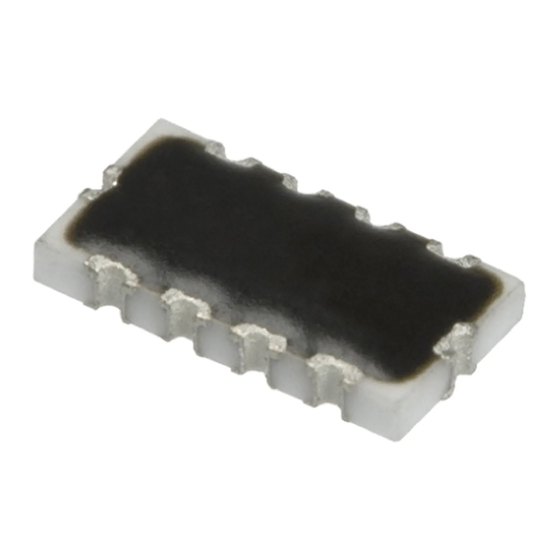
- Page 3 ■ Explanation of Part Numbers ● EZASSB (R/C Except the standard Com bi na tion) Common Code Thick Film Noise Suppression and 4.0 mm Filtering Components ■ Construction EZACT Marking Protective coating Alumina substrate Electrode (Outer) Electrode (Outer) EZANT Alumina substrate Marking Electrode (Outer)
- Page 4 ■ Dimensions in mm(not to scale) EZACT 0.5±0.1 2.0±0.1 0.30±0.15 0.20±0.15 Size : 0805 inches Mass (Weight) [1000 pcs.] :4 g EZAST/SS 0.5±0.2 0.8±0.1 4.0±0.2 0.45±0.20 0.4±0.2 Size : 1608 inches Mass (Weight) [1000 pcs.] :17 g EZASTB/SSB 0.58±0.2 0.4±0.2 0.25±0.15 0.65±0.10 4.0±0.2...
- Page 5 ■ Ratings Item Resistance Values Resistance Tolerance Temperature Coeffi cient of Resistance (T.C.R.) Rated Power Limiting Element Voltage (Maximum Rated Continuous Working Voltage) Capacitance Values (25 °C, 1 kHz , 1 Vrms) Capacitance Tolerance Capacitance Temperature Characteristics Dissipation Factor Rated Voltage Category Temperature Range (Operating Temperature Range) (1) For resistors operated in ambient temperature above 70 °C, rated power shall be derated.
- Page 6 ■ Packaging Methods (Taping) ● Standard Quantity Type Kind of Taping EZACT Punched Carrier Taping EZADT EZAST/SS EZASTB/SSB Embossed Carrier Taping EZANT ● Carrier Tape Type ±0.15 ±0.20 EZACT 1.65 2.40 ±0.20 ±0.20 EZADT 2.00 3.60 EZAST/SS ±0.20 ±0.20 2.50 4.40 EZASTB/SSB ±0.20...
- Page 7 ■ Recommended Land Pattern Design ●EZACT ●EZADT ●EZAST/SS ●EZASTB/SSB c d b ●EZANT • Design to make GND pattern as large as possible, because high frequency noise is removed from GND terminals of chip RC network. Design and specifi cations are each subject to change without notice. Ask factory for the current technical specifi cations before purchase and/or use. Should a safety concern arise regarding this product, please be sure to contact us immediately.
-
Page 8: Safety Precautions
■ Recommended Soldering Conditions Recommendations and precautions are described below. ● Recommended soldering conditions for refl ow ·R efl ow soldering shall be performed a maximum of two times. ·Please contact us for additional information when used in conditions other than those specifi ed. ·Please measure the temperature of the terminals and study every kind of solder and printed circuit board for solderability be fore actual use. - Page 9 Safety Precautions (Common precautions for EMI Filters, Fuses, and Sensors[MR Elements]) • When using our products, no matter what sort of equipment they might be used for, be sure to make a written agreement on the specifi cations with us in advance. The design and specifi cations in this catalog are subject to change without prior notice.