Kenwood DDX7032 Service Manual
Monitor with dvd receiver / navigation system
Hide thumbs
Also See for DDX7032:
- Installation manual (36 pages) ,
- Instruction manual (165 pages) ,
- Instruction manual (104 pages)
Table of Contents
Advertisement
MONITOR WITH DVD RECEIVER / NAVIGATION SYSTEM
DDX7032/7032M/712
DNX7120/7220/7320
SERVICE MANUAL
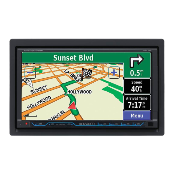
Illustrations is DNX7120
NAVIGA TION SYSTEM
*
DC cord
DC cord
(E30-6825-05)
(E30-6824-05)
PRK: (2m)
REV: (5m)
Remote controller assy
(A70-2082-15) RC-DV330 :DNX
(A70-2083-15) RC-DV340 :DDX
Size AAA battery
Not supplied
ILLUSTRATION IS
RC-DV340
The IC106 in the Digital I/O unit (X88-2030-11) are not replaceable components. When this
IC are defective, replace the whole Digital I/O unit (X88-2030-11).
The IC5,9,21 and IC60 in the DVD unit (X37-1120-06) are not replaceable components.
When these ICs are defective, replace the whole DVD mechanism assembly (X92-6180-01).
You cannot replace only the board.
* Depends on the models. Refer to the parts list.
*
Cord with pinplug(AV)
(E30-6792-05)
Escutcheon
Escutcheon
(B07-3224-01)
(B07-3172-12)
© 2008-4 PRINTED IN JA PAN
B53-0634-00 ( N ) 429
DNX7120
ANT module(GPS-ANT)
(W02-5305-05)
(5m)
Screw set
(N99-1779-15)
Cord with pinplug(PRE)
(E30-6794-05)
Cord with plug(ipod)
(E30-6785-05)
(1m)
*
Mounting hardware assy
(J22-0657-03)
This product uses Lead Free solder.
RoHS
This product complies with the
*
Mounting hardware
(J21-9867-04)
*
Adhesive double-
*
coated tape
(H30-0595-04)
*
Clamper
(J11-0660-05)
*
Cord with plug(relay)
(E30-6786-05)
(1m)
Lever
(D10-4589-04) x2
directive for the European market.
*
Advertisement
Table of Contents

Related Manuals for Kenwood DDX7032


Summary of Contents for Kenwood DDX7032
- Page 1 MONITOR WITH DVD RECEIVER / NAVIGATION SYSTEM DDX7032/7032M/712 DNX7120/7220/7320 SERVICE MANUAL © 2008-4 PRINTED IN JA PAN B53-0634-00 ( N ) 429 Illustrations is DNX7120 DNX7120 NAVIGA TION SYSTEM ANT module(GPS-ANT) Mounting hardware (W02-5305-05) (J21-9867-04) (5m) Screw set Adhesive double-...
-
Page 2: Block Diagram
DDX7032/7032M/712 DNX7120/7220/7320 BLOCK DIAGRAM DC CN (X34- ) iPod S/PDIF USB I/F (X88- ) (X15- ) (A/2) CN101 J502 J501 J500 J503 IC106 MEDIA PROCESSOR CN701 CN350 ACC DET IC302 IC104 IC901 NAVI RGB VIDEO CSYNC AUDIO NAVI SYNC NAVI TX/RX,etc... - Page 3 DDX7032/7032M/712 DNX7120/7220/7320 BLOCK DIAGRAM DNX8xx/DNX7xx ONLY DDX8xx/DNX8xx ONLY DDX812/8032BT/ (X16-636) (X17- ) DNX8120/ DDX8xx/ DDX7xx/DNX7xx DDX7xx ONLY DNX8220BT/ ONLY DNX7220 ONLY NAVI DSPxx SLOT NAVI I/F MINI DIN CODECxx CODECxx, ANT. ANT. CODEC DSPxx,etc DC CN TV I/F J650 W500...
- Page 4 (X37-112) DISC PDIC VCC DVD LD/CD LD IC21 VREFH KDP2C SPINDLE OPTICAL IMON/VR DVD/VR CD SW REG MOTOR PICKUP PDIC I/V OUT D1.2V IC39 THERMISTER FO+-,TR+- D3.3V IOPDET CONNECTOR D3.3V A3.3V HALL IC (30P) A3.3V V3.3V PLL3.3V E2PROM LO/EJ 2PHASE 27MHz Q12,13 DC MOTOR...
-
Page 5: Components Description
DDX7032/7032M/712 DNX7120/7220/7320 COMPONENTS DESCRIPTION ● VIDEO CONTROL UNIT (X15-115x-xx/X15-117x-xx) Ref. No. Application / Function Operation / Condition / Compatibility 5V regulator T_P+5V, BU_DET 3.3V regulator TILT3.3V 3.3V regulator TC3.3V IC200 DC-DC control IC DC-DC control (MECHA8V, V5V, SW5V (D5V)) IC201 DC-DC control IC DC-DC control (SW3.3V, P5V, USB5V) -
Page 6: Bass Management
DDX7032/7032M/712 DNX7120/7220/7320 COMPONENTS DESCRIPTION Ref. No. Application / Function Operation / Condition / Compatibility 9V regulator LED9V regulator Q48,49 TILT3.3V switch Q200 DC-DC protection control Q201 DC-DC output voltage switching Q202~204 DC-DC protection control Q205 DC-DC SW FET (5V or 8.0V) - Page 7 DDX7032/7032M/712 DNX7120/7220/7320 COMPONENTS DESCRIPTION Ref. No. Application / Function Operation / Condition / Compatibility 3-terminal regulator DSP_D3.3V POWER SUPPLY IC10 3-terminal regulator DSP_D1.25V POWER SUPPLY ● CONTROL CIRCUIT UNIT (X29-4490-xx) Ref. No. Application / Function Operation / Condition / Compatibility...
- Page 8 DDX7032/7032M/712 DNX7120/7220/7320 COMPONENTS DESCRIPTION Ref. No. Application / Function Operation / Condition / Compatibility IC701 Voltage detection IC μ-com reset voltage (3.5V) monitoring IC702 Pin100 μ-com Mainly control Audio board IC704 Power IC Power amplifi er for speaker output IC705...
- Page 9 DDX7032/7032M/712 DNX7120/7220/7320 COMPONENTS DESCRIPTION Ref. No. Application / Function Operation / Condition / Compatibility Q706 Transistor DET MUTE circuit (Trigger Reset) Q707 Transistor AV selector control circuit ● VIDEO UNIT (X35-4940-xx) Ref. No. Application / Function Operation / Condition / Compatibility...
- Page 10 DDX7032/7032M/712 DNX7120/7220/7320 COMPONENTS DESCRIPTION Ref. No. Application / Function Operation / Condition / Compatibility IC202,203 SDRAM 256Mbit SDRAM for work memory IC207 iPod Authentication Coprocessor iPod Authentication IC211 NOR Flash Memory 256Mbit Flash Memory for program data and graphic data...
-
Page 11: Microcomputer's Terminal Description
DDX7032/7032M/712 DNX7120/7220/7320 MICROCOMPUTER’S TERMINAL DESCRIPTION ● SYSTEM MICROCOMPUTER: 30878MJBA24GP (X15: IC404) True Value Pin No. Pin Name Application Processing Operation Description Table AV_SDA/TC_ Communication data between AV_SW, T/C, and SDA/E2P_SDA Hsync input: For VCOM adjustment input from X35 MIX_REMO Remote controller data input SYS_MDATA Data output to AUDIO μ-com... - Page 12 DDX7032/7032M/712 DNX7120/7220/7320 MICROCOMPUTER’S TERMINAL DESCRIPTION True Value Pin No. Pin Name Application Processing Operation Description Table BUSY Terminal for writing data in μ-com DVD_SDA I/O Communication data with DVD mechanism DVD_SCL Communication clock with DVD mechanism DISC_DET Disc detection L: Detected (Disc is found)
- Page 13 DDX7032/7032M/712 DNX7120/7220/7320 MICROCOMPUTER’S TERMINAL DESCRIPTION True Value Pin No. Pin Name Application Processing Operation Description Table VCC2 Power ON/OFF control H: Power ON MCNT Switching of tilt mechanism power supply voltage H: 8V, L: 5V JIGU_EJ Operable without tilt mechanism...
-
Page 14: Truth Value Table
DDX7032/7032M/712 DNX7120/7220/7320 MICROCOMPUTER’S TERMINAL DESCRIPTION Truth value table q Destination setting w SW truth value table Audio switching Destina- MODEL Category TYPE3 TYPE2 TYPE1 TYPE0 tion MAIN L/R output SW Pin No Terminal name AOUT_SW1 AOUT_SW2 M/M2 Control IC TC4052BFT (IC502) - Page 15 DDX7032/7032M/712 DNX7120/7220/7320 MICROCOMPUTER’S TERMINAL DESCRIPTION ● AUDIO MICROCOMPUTER: 30624MWPB74GP (X34: IC702) True Value Pin No. Pin Name Application Processing Operation Description Table Control of peripheral power supply H: ON, L: OFF P_CON PCON control H: EXCEPT, L: When STANDBY or POWER OFF...
- Page 16 DDX7032/7032M/712 DNX7120/7220/7320 MICROCOMPUTER’S TERMINAL DESCRIPTION True Value Pin No. Pin Name Application Processing Operation Description Table SAT_RX Communication with SAT EM_CLK Communication with emulator BUSY Output of BUSY signal during writing-in SYS_SDATA Communication between μ-coms SYS_MDATA Communication between μ-coms SYS_MCLK Communication between μ-coms...
- Page 17 DDX7032/7032M/712 DNX7120/7220/7320 MICROCOMPUTER’S TERMINAL DESCRIPTION True Value Pin No. Pin Name Application Processing Operation Description Table E2P_SCL E2P control I2C CLK AUD_SCL EVOL control I2C CLK E2P_SDA I/O E2P control I2C DATA AUD_SDA I/O EVOL control I2C DATA A_WRT_E2P E2P writing-in control...
- Page 18 DDX7032/7032M/712 DNX7120/7220/7320 MICROCOMPUTER’S TERMINAL DESCRIPTION Truth value table q Destination setting TYPE0 Setup Voltage (Power supply voltage = 5) Destina- Actual Actual Settings for μ-com MODEL Category TYPE3 TYPE2 TYPE1 TYPE0 tion pull down pull up re- Destination Mid point...
- Page 19 DDX7032/7032M/712 DNX7120/7220/7320 MICROCOMPUTER’S TERMINAL DESCRIPTION True Value Pin No. Pin Name Application Processing Operation Description Table IPOD_POW (NC) Authentication chip power supply control (Not used) #WAIT WAIT input (Not used) USB2_NEG I/O USB2 data (Not used) AD25 Address bus #CS2...
- Page 20 DDX7032/7032M/712 DNX7120/7220/7320 MICROCOMPUTER’S TERMINAL DESCRIPTION True Value Pin No. Pin Name Application Processing Operation Description Table EP_MREQ SysCom communication request DA28 I/O Data bus #EP_INI Reset start notifi cation AD16 Address bus (ETHER I/F for design) RXERR (ETHER I/F for design)
- Page 21 DDX7032/7032M/712 DNX7120/7220/7320 MICROCOMPUTER’S TERMINAL DESCRIPTION True Value Pin No. Pin Name Application Processing Operation Description Table G6,12 GND R USB0_ERR 5V over current detection in USB0 L: Over current is detected. L: Over current is detected. G15,16 SUB_CLK Sub clock input...
- Page 22 DDX7032/7032M/712 DNX7120/7220/7320 MICROCOMPUTER’S TERMINAL DESCRIPTION True Value Pin No. Pin Name Application Processing Operation Description Table Address bus I/O Data bus L6,12 GND R L13,14 PLL_GND Main oscillator GND XTALI Main clock 14.7456MHz XTALO Main clock 14.7456MHz Address bus #DQM1...
- Page 23 DDX7032/7032M/712 DNX7120/7220/7320 MICROCOMPUTER’S TERMINAL DESCRIPTION True Value Pin No. Pin Name Application Processing Operation Description Table I2C_SDA I/O Communication data (I2C) I2C_SDA Test mode select G_LED Green LED R_LED Red LED EPI_BTO BT→EP9307 communication data UART_RDX2 SysCom communication data E_G3...
- Page 24 DDX7032/7032M/712 DNX7120/7220/7320 MICROCOMPUTER’S TERMINAL DESCRIPTION True Value Pin No. Pin Name Application Processing Operation Description Table I/O Data bus (JTAG I/F for design) U12-14 (UART I/F for design) USB1_NEG I/O USB1 data Truth value table q Watch dog startup #CS1...
-
Page 25: Test Mode
DDX7032/7032M/712 DNX7120/7220/7320 TEST MODE 3. Screen transition This Test mode is applicable to models that are listed in Table 1. The system is started with the Test Mode Main screen when Class Series Model Name Destination it is started in the Test mode. When the system is trans-... -
Page 26: Service Screen
DDX7032/7032M/712 DNX7120/7220/7320 TEST MODE 4.3. Service screen Key Specifi cation Information : Transfer to Information screen. This screen shows a variety of service information. Press- Service : Transfer to Service screen. ing each [Clear] key clears the data saved in the nonvolatile Direct Select : Transfer to Direct Select screen. - Page 27 DDX7032/7032M/712 DNX7120/7220/7320 TEST MODE 4.5. Tuner Mute Level Adjust screen • DVD DivX Registration Code Display DivX Registration Code, and clear the Code with Adjust the Mute Level stored in the E2PROM of the Tuner F/E. [Clear] key. The Tuner Mute Level Adjust screen is shown in Figure 4.5.
- Page 28 DDX7032/7032M/712 DNX7120/7220/7320 TEST MODE Touch Adjust iPod Check Touch Adjust iPod Check 1-point being input 2-point being input Cancel Wite OK/NG iPod Check iPod OK/NG 3-point being input 4-point being input Cancel Return Return Figure 4.7 Touch Adjust screen Figure 4.9 iPod Authentication Chip Confi rmation screen Key Specifi...
- Page 29 DDX7032/7032M/712 DNX7120/7220/7320 TEST MODE 4.12. Tilt Mecha Position Adjust screen • Start the LOOPBACK test when “Complete” is displayed in the stats display area. Adjust the panel mechanism position from this screen. • After the completion of the LOOPBACK test, press [Clear] The Tilt Mecha Position Adjust screen is displayed in Figure key to initialize the flash memory and to set “0000”...
-
Page 30: Functional Specification
DDX7032/7032M/712 DNX7120/7220/7320 TEST MODE The mode of the remote controller shall be “AUDIO”. Parrot Check Parrot Check Function DVD video mode DVD audio mode Parrot Check Parrot OK/NG Tenkey0 Flicker Adjustment Tenkey1 Tilt mechanism position adjustment Cancel Return Tenkey2 DC Offset check Figure 4.14 Parrot Check screen... -
Page 31: Screen Adjustment
DDX7032/7032M/712 DNX7120/7220/7320 TEST MODE 5.7. DVD • When there is Digital Out terminal, the setting shall be such that the output is always On. • Use CD media KTD-02A, DVD media TDV-540A/TTD-100 • The default setting of Line Mute shall be On. -
Page 32: Flicker Adjustment
DDX7032/7032M/712 DNX7120/7220/7320 TEST MODE 5.13. Flicker adjustment 5.17. Security Code writing-in q Use Tenkey 0 on the remote controller to turn the Flicker • When entering the Security Code that is defi ned as a pair adjustment On. of the serial number of the product (for other destinations... -
Page 33: Adjustment Of Horizontal Display Start Position And Pixel
DDX7032/7032M/712 DNX7120/7220/7320 ADJUSTMENT 1. Flicker adjustment w After the automatic adjustment, “Auto Set OK” will be shown to indicate the completion of the adjustment. ● Condition Video source: Video 3. Adjustment of Horizontal display start Video: Luster white 30%~50% position and pixel... - Page 34 DDX7032/7032M/712 DNX7120/7220/7320 ADJUSTMENT • DNX_NAVI Adjustment screen Procedure to display NAVI Adjustment screen q Start the set. w Connect special jig on MINI_USB of NAVI. ● Adjustment Procedure • Display Range Adjustment: DOT FREQ q Press HPOSI on the Test Mode Main screen.
- Page 35 DDX7032/7032M/712 DNX7120/7220/7320 ADJUSTMENT Enlarge NG w-2-1: DNX_NAVI • Screen Position Adjustment: HPOSI Adjust the Screen Adjustment key so that the NAVI screen becomes horizontally symmetrical. • Pixel Adjustment: DOT PHASE Adjust the Pixel Adjustment key so that the screen be- Adjust the key so that the width of the comes gray.
- Page 36 DDX7032/7032M/712 DNX7120/7220/7320 ADJUSTMENT w-2-2: DDX_NAVI KNA-G520 Enlarge OK Adjust the Screen Adjustment key so that the NAVI screen becomes horizontally symmetrical. Adjust the key so that the width of the left gap is same as that of right gap. Enlarge OK...
-
Page 37: Touch Panel Adjustment
DDX7032/7032M/712 DNX7120/7220/7320 ADJUSTMENT e After adjustment is completed for 4 areas, if “Write OK” is displayed, the adjustment is completed. Press Return to exit from the Touch screen. Cancel Cancel Enlarge NG Cancel Cancel ∗ If the center of “+” mark wasn’t pressed accurately, press Cancel to start over the adjustment. -
Page 38: Pc Board (Component Side View)
DDX7032/7032M/712 DNX7120/7220/7320 PC BOARD (COMPONENT SIDE VIEW) DIGITAL I/O UNIT X88-2030-11 (J76-0512-12) CN210 C911 R900 R202 R268 R286 R203 R267 C264 R707 R708 R291 C227 C228 IC200 R200 R906 IC207 C201 IC100 IC101 R297 C275 R248 R249 R116 R250 R118... - Page 39 DDX7032/7032M/712 DNX7120/7220/7320 PC BOARD (FOIL SIDE VIEW) DIGITAL I/O UNIT X88-2030-11 (J76-0512-12) P310 P309 R509 IC203 IC202 CP142 CP140 CP127 CP126 IC108 R146 R145 IC211 R522 CP108 CP160 CP109 C119 CP106 C116 CP107 C124 C115 C122 C144 R140 C117 R197...
- Page 40 DDX7032/7032M/712 DNX7120/7220/7320 PC BOARD (COMPONENT SIDE VIEW) CN500 C850 CN850 IC505 VIDEO CONTROL UNIT X15-117x-xx A/2 (J76-0508-12) J503 Q500 C531 R540 C524 R506 R521 Q501 IC502 R543 C115 R523 C700 P101 IC700 D501 P105 R474 C129 G S S S...
- Page 41 DDX7032/7032M/712 DNX7120/7220/7320 X15-117x-xx Ref. No. Address IC400 IC402 IC405 P103 IC501 J502 J501 J500 IC502 R537 R533 IC504 R529 R520 R528 IC505 IC600 R571 R572 IC609 R573 R518 R519 10 6 IC700 C518 X15 B/2 D501 C517 R507 IC504 C129...
- Page 42 DDX7032/7032M/712 DNX7120/7220/7320 PC BOARD (FOIL SIDE VIEW) TP500 Q700 R710 VIDEO CONTROL UNIT X15-117x-xx A/2 (J76-0508-12) TP506 TP724 R542 TP775 Q508 R541 TP766 TP770 TP18 R909 TP764 R550 TP19 Q507 TP768 TP17 TP15 D504 R548 TP511 TP510 X15 B/2 TP797...
- Page 43 DDX7032/7032M/712 DNX7120/7220/7320 X15-117x-xx Ref. No. Address TP18 IC200 IC201 TP22 IC404 TP23 TP20 IC601 IC604 IC606 TP21 IC608 TP11 IC612 TP14 TP13 O G I TP10 TP790 TP786 TP202 TP201 TP205 Q201 R205 R204 R288 R208 R234 C203 C204 R238...
- Page 44 DDX7032/7032M/712 DNX7120/7220/7320 PC BOARD (COMPONENT SIDE VIEW) VIDEO UNIT X35-4940-11 A/2 (J76-0511-12) X35 B/2 R638 R637 R509 C502 Q500 C500 R111 C501 R501 R500 C124 C115 C122 C121 C120 C102 L101 L102 D100 C101 IC101 C109 C110 R109 R100 IC100...
- Page 45 DDX7032/7032M/712 DNX7120/7220/7320 PC BOARD (FOIL SIDE VIEW) X35 B/2 VIDEO UNIT X35-4940-11 A/2 (J76-0511-12) R142 Q141 Q140 D611 R609 C603 R608 X35-4940-11 D610 R604 D608 Ref. No. Address R603 IC200 Q600 R606 IC300 R605 Q140 C207 R621 R207 Q141 R623...
-
Page 46: Electric Unit
DDX7032/7032M/712 DNX7120/7220/7320 PC BOARD (COMPONENT SIDE VIEW) ELECTRIC UNIT X34-598x-xx (J76-0509-12) CN700 R807 R806 R805 R804 R801 C126 R803 R575 D550 D556 R568 R564 R567 R574 Q119 R566 R139 R571 C123 R572 R138 R573 D557 D601 C550 C551 IC104 Q705 Q707... - Page 47 DDX7032/7032M/712 DNX7120/7220/7320 X34-598x-xx Ref. No. Address IC101 IC104 IC106 D650 J650 IC200 J600 D651 IC201 IC203 D608 IC500 C617 IC550 D601 P500 IC650 W500 Q707 IC701 D609 IC702 R211 IC704 R501 R666 R665 C210 R659 R660 C211 C654 R658 C507...
- Page 48 DDX7032/7032M/712 DNX7120/7220/7320 PC BOARD (FOIL SIDE VIEW) ELECTRIC UNIT X34-598x-xx (J76-0509-12) R667 R613 R668 R669 R578 R132 R133 R577 R565 R576 R563 R562 C616 C618 R612 R560 R558 R556 C218 R206 C217 R115 C522 R779 C247 R751 R798 IC303 C504...
- Page 49 DDX7032/7032M/712 DNX7120/7220/7320 X34-598x-xx Ref. No. Address IC103 Q104 R562 R561 Q107 Q108 Q111 Q112 Q113 R556 Q114 Q116 Q117 Q118 Q500 Q700 Q701 Q702 Q704 C112 Q706 R125 R115 R110 C277 R124 C133 R107 Q104 IC103 DAUGHTER UNIT O G I...
- Page 50 DDX7032/7032M/712 DNX7120/7220/7320 PC BOARD (COMPONENT SIDE VIEW) CONTROL CIRCUIT UNIT X29-4490-11 (J76-0510-12) R207 C133 R206 D111 R155 R156 Q203 R219 R218 Q210 Q206 Q209 CN302 C105 R113 C104 C117 C110 C114 C127 D101 C126 D100 C120 C131 C132 C123 C124...
- Page 51 DDX7032/7032M/712 DNX7120/7220/7320 PC BOARD (FOIL SIDE VIEW) CONTROL CIRCUIT UNIT X29-4490-11 (J76-0510-12) Q114 Q115 TP363 C141 R164 R165 D112 TP200 C143 C142 R223 TP201 C138 Q113 C140 R161 TP354 TP369 R101 TP356 R100 TP113 R115 TP112 TP111 TP110 R116 TP109...
- Page 52 DDX7032/7032M/712 DNX7120/7220/7320 PC BOARD (COMPONENT SIDE VIEW) DVD UNIT X37-1120-06 (J76-0162-22) C413/ C459 R574 C412 R450 R498 C402 C401 CP62 R587 CP63 CP64 CP65 R490 R556 C493 R557 C494 R558 C495 C478 IC53 R559 C496 IC31 IC27 DGND IC54 R623...
- Page 53 DDX7032/7032M/712 DNX7120/7220/7320 PC BOARD (FOIL SIDE VIEW) DVD UNIT X37-1120-06 (J76-0162-22) C479 CN10 CN11 C477 CP54 CP55 R468 CP58 CP57 CP59 CP56 CP44 R472 CP66 R470 C484 R547 C510 R522 SDAT C482 R545 CP68 R521 C481 R544 3.3V C450 C148...
- Page 54 DDX7032/7032M/712 DNX7120/7220/7320 PC BOARD PC BOARD (COMPONENT SIDE VIEW) (FOIL SIDE VIEW) SWITCH UNIT SWITCH UNIT X16-6280-10 X16-6280-10 (J86-0050-15) (J86-0050-15) SUB-CIRCUIT UNIT X16-6360-10 (J76-0515-12) only DNX X16-6280-10 Ref. No. Address Refer to the schematic diagram for the values of resistors and capacitors.
- Page 55 DC CORD DC CORD (E30-6824) (E30-6825) K,M,R,X TYPE E,E2 TYPE FRONT L REAR L WHT/BLK GRN/BLK GRY/BLK VIOL/BLK FRONT R REAR R VIOL VIO/WHT 12 13 14 15 16 REVERSE 11 10 9 LGRN PRK SW LBLU REMO CONT PNK/BLK ANT CONT EXT.CONT BLU/WHT...
- Page 56 DDX7032/7032M/712 DNX7120/7220/7320 (X88-2030-1x) P305 P306 P310 P309 CN210 16 17 20 21 CN328 USB SHELD GND A GND TP392 A GND TP251 TP394 DGND AUDIO1 L A GND TP393 AUDIO1 R 5V REG. A GND 8.0V IC902 A GND R481...
- Page 57 DDX7032/7032M/712 DNX7120/7220/7320 EXCLUSIVE OR GATE SW3.3V 1.8V REG 0-3.3V IC104 0-3.3V IC105 3.3V 3.3V 0-3.3V IC108 3.3V 0-3.3V C149 NOR FLASH MEMORY 128Mbit R710 INVERTER DGND IC211 CP128 10K L AD24 NC56 L AD23 0-3.3V NC55 SW3.3V L AD16 SPCLK 3.3V...
- Page 58 DDX7032/7032M/712 DNX7120/7220/7320 1.8V SW3.3V 1.8V REG. R112 2.2K C105 R109 R115 MEDIA PROCESSOR 2.2K IC106 C106 (BOTTOM VIEW) TP101 0-3.3V 0-3.3V 0-3.3V E G2 E B4 E B1 0-3.3V 0-3.3V 0-3.3V 0-3.3V 0-3.3V E G1 E B2 CP147 10K 0-3.3V 0-3.3V...
- Page 59 DDX8032BTM may vary slight ly due to DNX8120 DNX8220BT vari a tions between in di- DDX712 DDX7032 vid u al in stru ments or/and DDX7032M 30-11 DNX7120 units. 0-3.3V DNX7220 R601 R602 DNX7032 SW3.3V 1.8V DDX7032/7032M/712, DNX7120/7220/7320 (1/6) X88-2030-11 (4/4)
- Page 60 DDX7032/7032M/712 DNX7120/7220/7320 X35- A/2- CN100 X34- CN300 CN700 68 67 66 65 64 63 62 61 60 59 58 57 56 55 54 53 52 51 50 49 48 47 46 45 44 43 42 41 40 39 38 37 36 35 34...
- Page 61 DDX7032/7032M/712 DNX7120/7220/7320 (X15-115/117x-xx) (A/2) P102 P106 26 25 24 23 22 21 20 19 18 17 16 15 14 13 12 11 10 9 8 7 6 5 4 3 2 D702 D706 D703 D707 C709 C716 DGND 100u25 D704...
- Page 62 DDX7032/7032M/712 DNX7120/7220/7320 C430 C435 2200P 4.8V 5.0V 3.4V R564 100 INV SW NT/PAL OUT TP438 R461 100K RGB/COMP TP439 3.3V OPEN/CLOSE TP427 TP426 TC3. 3.2V 5.0V TP406 TP437 R427 100 R434 WRT E2P TP425 TP431 TP424 TP412 TP421 TP413 R485 100...
- Page 63 DDX7032/7032M/712 DNX7120/7220/7320 X34- CN350 ∗ to BT MO SPDIF CN504 J503 CN701 ∗ 50 49 48 47 46 45 44 43 42 41 40 39 38 37 36 34 33 32 31 30 29 28 27 26 25 24 23 22 21 20 19 18 17 16 15 14 13 12 11 10 9 8...
- Page 64 B LINE to DVD MECHA . (X37-1120-03) CN6 DDX7032/7032M/712, DNX7120/7220/7320 (2/6) • DC voltages are as measured with a high impedance volt me ter. Val ues may vary slight ly due to vari a tions between in di vid u al in stru ments or/and units.
- Page 65 DDX7032/7032M/712 DNX7120/7220/7320 (X35-4940-1x) (A/2) +5V-1 L103 3.3uH D101 D102 +5V-1 +5V-1 L201 L104 3.3uH L200 R108 10uH 10uH L105 D103 10uH IC102 5.0V TP+5V 5.0V IC100 C122 5.0V C112 C119 0.01 C106 SHDN 1.4V D100 1000P L100 15.0V C121 10uH 5.0V...
- Page 66 DDX7032/7032M/712 DNX7120/7220/7320 to LCD PANEL +5V-1 +5V-1 +15V-1 +15V-1 L201 TP361 10uH R210 VCOM TP201 TP202 L203 +12.5V 10uH R203 VR200 VCOM AMP C122 Q141 0.01 Q202 IC200 R206 R212 C372 C121 2.2K -12.0V Q205 R209 C120 VCOM Q140 Q203 TP360 12.5V...
- Page 67 • DC voltages are as mea- sured with a high imped- ance volt me ter. Val ues may 750K vary slight ly due to vari a- tions between in di vid u al in stru ments or/and units. DDX7032/7032M/712, DNX7120/7220/7320 (3/6) X35-4940-11 (3/3), X16-6280-10 (1/1)
- Page 68 DDX7032/7032M/712 DNX7120/7220/7320 (X34-584x-xx/598x-xx) to DC CORD X15- A/2- ∗ CN550 CN300 ∗ C17 0.015 TP23 0.01 0.01 TILT3.3V 3900u25 TP24 SURGE PARK 4.7K R4 4.7K 6.2K ∗ C3 0.01 C8 0.01 6.2K 3.3u50 1/2W 100K 0.01 0.47 9.1K ∗ L MUTE...
- Page 69 DDX7032/7032M/712 DNX7120/7220/7320 to NAVI BOARD ∗ J550 NAVIGATION to TV TUNER J600 NAVI SYNC TP585 D606 D600 ∗ ∗ R574 910 R564 1K D607 VGND ∗ R565 C616 0.1 D601 ∗ R571 910 ∗ R563 D608 ∗ R572 910 ∗...
- Page 70 DDX7032/7032M/712 DNX7120/7220/7320 X29- X29- CN300 to TV TUNER CN401 CN400 R613 AGND VGND AGND VGND ESDGND D604 ESD2 D605 D613 SEL A5V-1 C218 C221 NAVI-CMP C219 AVSAGND C222 VIN5 C201 2.2 SUB-L LIN+2 IICN C202 2.2 SUB-R RIN+2 VIN4 C213 2.2...
- Page 71 DDX7032/7032M/712 DNX7120/7220/7320 ∗ ANT. ∗ W500 6 3 2 ∗ C520 IC202 1000P A8V-2 8.0V 4.0V 8.0V IC201 4.0V 4.0V VGND VGND VGND R202 AV I-R ∗ R245 6.8K FM/AM AV I-L FRONT E AV I-G AV O-V C522 1000 ∗...
- Page 72 DDX7032/7032M/712 DNX7120/7220/7320 (X89-3062-71) DNX7220, DNX8220BT P500 ONLY P501 ∗ A500 R800 100K DET MUTE BU5V Q704 Q706 0.15uH Q701 R798 C518 C519 C516 C517 0.01 0.01 0.01 0.01 FM/AM FRONT END C508 C509 C506 C507 10u16 22u16 R795 22u16 22u16...
- Page 73 • DC voltages are as measured with a high impedance volt me ter. Val ues may vary slight ly due to vari a tions between in di vid u al in- P743 EM CLK stru ments or/and units. A RESET DDX7032/7032M/712, DNX7120/7220/7320 (4/6) X34-598x-xx (6/6), X89-3062-71 (2/2)
- Page 74 DDX7032/7032M/712 DNX7120/7220/7320 AV OUT/AV IN (X29-449x-xx) CN300 R4 1K BCAM VG C1 0.01 C18 0.1 BCAM V ∗ BCAM VG R5 1K AVIN2 VG ∗ C2 0.01 C19 0.1 AVIN2 V AVIN2 VG ∗ AVIN1 VG AVIN1 V AVIN1 VG...
- Page 75 1000P 1000P 1000P Q107 Q105 Q104 Q103 Q102 Q100 Q116 ∗ Q106 Q101 PRE MUTE BU5V DDX7032/7032M/712, DNX7120/7220/7320 (5/6) (X29-449x-xx) R5,12,18,21, IC100-102 : NJM4565V-ZB D1-3,18 : STZ6.2N UNIT MODEL NAME R132 7-9,11 27,127,128 IC103 : ICL7660SIBAZ D4,6 : UDZS8.2B DDX812 D5,8 : UDZS6.2B...
- Page 76 DDX7032/7032M/712 DNX7120/7220/7320 (X17-2030-10) only DDX8.., DNX8... 5.6K 0.01 180P LP AGND 3.3V LP AGND A3.3V A3.3V RLP AGND 40 10u16 SUB IN RLP AGND 3.3V AGND 680P 3.3V C IN FLP AGND BASS MANAGEMENT SW TP10 RR IN FLP AGND 0.01...
- Page 77 PLLP VDD DAT2 ance volt me ter. Val ues may vary slight ly due to DAT2 3.3V vari a tions between in di vid u al in stru ments or/and units. D1.25V D3.3V DDX7032/7032M/712, DNX7120/7220/7320 (6/6) X17-2030-10 (2/2), X16-6360-10 (1/1)
- Page 78 DDX7032/7032M/712 DNX7120/7220/7320 (X37-1120-0x) 3.3V ∗ R471 CN10 RESET ∗ DGND CP44 33 ∗ 128M SDRAM IC54 3.3V C479 VDD1 VSS3 3.3V CP63 DQ15 3.3V VSSQ4 VCCQ1 DQ14 CP54 33 DQ13 3.3V C478 VCCQ4 VSSQ1 DD10 VSS 1 DQ12 DQ11 DD11 3.3V...
- Page 79 DDX7032/7032M/712 DNX7120/7220/7320 D1.2V 3.3V 3.3V TP230 CP69 22 R513 ∗ IC27 1.8V C100 VSS1 3.3V VDD33 1 CP4 47 3.3V LRCKI NCAS BCKI NRAS NCSM TRST 3.3V CP3 47 VSS 56 MA11 VDD2 55 C415 IC31 C101 ATRAC3 PORT RLRCK...
- Page 80 DDX7032/7032M/712 DNX7120/7220/7320 D1.2V D1.2V 3.3V TP153 TP240 R400 3.3V SCLOCK R401 4 3.3V SDATA R402 4 TP175 EXTRG0 3.3V 3.3V TP168 (ADATAIN) EXTRG1 TP169 (BCKIN) TRCCLK TP170 (LRCKIN) TRCDATA0 R491 750 TP208 (MONI AS) TRCDATA1 R492 750 TP209 (MONI FE) TRCDATA2...
- Page 81 DDX7032/7032M/712 DNX7120/7220/7320 ∗ ∗ D1.2V D1.2V D1.2V 3.3V 3.3V 3.3V VIDEO AMP C440 VIDEO SIGNAL IC12 VIDEO SIGNAL C223 IC53 3.3V R204 3.3V 5.0V TP176 C224 R400 R411 ∗ TP252 3.3V R490 0.01 5.0V TP228 C226 R587 TP174 R401 47...
- Page 82 DDX7032/7032M/712 DNX7120/7220/7320 : MN2DS0016AAUB : S29AL32D70TFI : S-24CS04AFT IC10 : AN41250A-VB TA78L05F-F IC12 : MM1671XNRE IC15 : AK4396VF ∗ IC21 : LTC3548EDD-F IC27 : NJM2865F318ZB IC31 : LC82360-E 3.3V IC39 : NJU7042 IC53 ∗ CN11 IC42 : TC74HC273FT 3.3V IC49...
-
Page 83: Exploded View (Dvd Mechanism)
DDX7032/7032M/712 DNX7120/7220/7320 EXPLODED VIEW (DVD MECHANISM) M1.7x2 : N09-6382-05 : N09-6408-15 φ1.7x4 M2x2 : N09-6426-15 : N09-6104-05 φ2x10 Inscriptions (register marks) on gears Align 6 marks as shown in the figure Drive gear 5 Drive gear 4C Parts with the exploded numbers larger than 700 are not supplied. -
Page 84: Exploded View (Unit)
DDX7032/7032M/712 DNX7120/7220/7320 EXPLODED VIEW (UNIT) N86-2605-48 φ2.6x5 M2.6x4 N35-2604-43 PANEL SCREW N09-6490-05 M3x11 N09-6498-05 M2.6x27 N09-6491-05 M2.6x5 N09-6493-05 M2.6x6 N09-6494-05 M3x5 N09-6425-15 N09-6727-05 φ3x8 (X15-) (B/2) VME1 (X89) (X34) W500 (X88-203) (X34-598) (X89-306) (X89) (X34) A501 (X15-) (A/2) (X29-449) (NAVI) -
Page 85: Exploded View (Panel)
DDX7032/7032M/712 DNX7120/7220/7320 EXPLODED VIEW (PANEL) Illustrations is RC-DV340 SIZE AAA BATTERY (NOT SUPPLIED) M2x3 N09-6489-05 WASHER (1.2x3.2) N19-2332-04 M2x3 N35-2003-48 (X35-) (B/2) (X35-)(A/2) LCD1 (X16-628) FPC2 (X16-628) Depends on the models. Refer to the parts list. Parts with the exploded numbers larger than 700 are not supplied. - Page 86 DDX7032/7032M/712 DNX7120/7220/7320 EXPLODED VIEW (DRIVE MECHANISM) M2x2.5 N09-6361-05 M1.7x3.7 N09-6363-05 M2x2.5 N09-6375-05 M2x3.5 N09-6376-05 M2x2.5 N09-6377-05 N09-6378-05 φ2x2 M2.6x4 N09-6379-05 WASHER N19-2321-04 Parts with the exploded numbers larger than 700 are not supplied.
-
Page 87: Parts List
E2 : DNX7220 (Europe) Indicates safety critical com po nents. K1 : DDX712 K2 : DNX7120 (North America) X2 : DDX7032 X3 : DNX7320 (Australia) R2 : DDX7032 (Latin America) M2 : DDX7032 M4 : DDX7032M M5 : DNX7320 (Other Areas) - Page 88 E2 : DNX7220 (Europe) Indicates safety critical com po nents. K1 : DDX712 K2 : DNX7120 (North America) X2 : DDX7032 X3 : DNX7320 (Australia) R2 : DDX7032 (Latin America) M2 : DDX7032 M4 : DDX7032M M5 : DNX7320 (Other Areas)
-
Page 89: Video Control Unit (X15-117X-Xx)
E2 : DNX7220 (Europe) Indicates safety critical com po nents. K1 : DDX712 K2 : DNX7120 (North America) X2 : DDX7032 X3 : DNX7320 (Australia) R2 : DDX7032 (Latin America) M2 : DDX7032 M4 : DDX7032M M5 : DNX7320 (Other Areas) - Page 90 E2 : DNX7220 (Europe) Indicates safety critical com po nents. K1 : DDX712 K2 : DNX7120 (North America) X2 : DDX7032 X3 : DNX7320 (Australia) R2 : DDX7032 (Latin America) M2 : DDX7032 M4 : DDX7032M M5 : DNX7320 (Other Areas)
- Page 91 E2 : DNX7220 (Europe) Indicates safety critical com po nents. K1 : DDX712 K2 : DNX7120 (North America) X2 : DDX7032 X3 : DNX7320 (Australia) R2 : DDX7032 (Latin America) M2 : DDX7032 M4 : DDX7032M M5 : DNX7320 (Other Areas)
- Page 92 E2 : DNX7220 (Europe) Indicates safety critical com po nents. K1 : DDX712 K2 : DNX7120 (North America) X2 : DDX7032 X3 : DNX7320 (Australia) R2 : DDX7032 (Latin America) M2 : DDX7032 M4 : DDX7032M M5 : DNX7320 (Other Areas)
- Page 93 E2 : DNX7220 (Europe) Indicates safety critical com po nents. K1 : DDX712 K2 : DNX7120 (North America) X2 : DDX7032 X3 : DNX7320 (Australia) R2 : DDX7032 (Latin America) M2 : DDX7032 M4 : DDX7032M M5 : DNX7320 (Other Areas)
-
Page 94: Switch Unit (X16-6280-10)
E2 : DNX7220 (Europe) Indicates safety critical com po nents. K1 : DDX712 K2 : DNX7120 (North America) X2 : DDX7032 X3 : DNX7320 (Australia) R2 : DDX7032 (Latin America) M2 : DDX7032 M4 : DDX7032M M5 : DNX7320 (Other Areas) -
Page 95: Electric Unit (X34-598X-Xx)
E2 : DNX7220 (Europe) Indicates safety critical com po nents. K1 : DDX712 K2 : DNX7120 (North America) X2 : DDX7032 X3 : DNX7320 (Australia) R2 : DDX7032 (Latin America) M2 : DDX7032 M4 : DDX7032M M5 : DNX7320 (Other Areas) - Page 96 E2 : DNX7220 (Europe) Indicates safety critical com po nents. K1 : DDX712 K2 : DNX7120 (North America) X2 : DDX7032 X3 : DNX7320 (Australia) R2 : DDX7032 (Latin America) M2 : DDX7032 M4 : DDX7032M M5 : DNX7320 (Other Areas)
- Page 97 E2 : DNX7220 (Europe) Indicates safety critical com po nents. K1 : DDX712 K2 : DNX7120 (North America) X2 : DDX7032 X3 : DNX7320 (Australia) R2 : DDX7032 (Latin America) M2 : DDX7032 M4 : DDX7032M M5 : DNX7320 (Other Areas)
- Page 98 E2 : DNX7220 (Europe) Indicates safety critical com po nents. K1 : DDX712 K2 : DNX7120 (North America) X2 : DDX7032 X3 : DNX7320 (Australia) R2 : DDX7032 (Latin America) M2 : DDX7032 M4 : DDX7032M M5 : DNX7320 (Other Areas)
- Page 99 E2 : DNX7220 (Europe) Indicates safety critical com po nents. K1 : DDX712 K2 : DNX7120 (North America) X2 : DDX7032 X3 : DNX7320 (Australia) R2 : DDX7032 (Latin America) M2 : DDX7032 M4 : DDX7032M M5 : DNX7320 (Other Areas)
-
Page 100: Video Unit (X35-4940-11)
E2 : DNX7220 (Europe) Indicates safety critical com po nents. K1 : DDX712 K2 : DNX7120 (North America) X2 : DDX7032 X3 : DNX7320 (Australia) R2 : DDX7032 (Latin America) M2 : DDX7032 M4 : DDX7032M M5 : DNX7320 (Other Areas) - Page 101 E2 : DNX7220 (Europe) Indicates safety critical com po nents. K1 : DDX712 K2 : DNX7120 (North America) X2 : DDX7032 X3 : DNX7320 (Australia) R2 : DDX7032 (Latin America) M2 : DDX7032 M4 : DDX7032M M5 : DNX7320 (Other Areas)
- Page 102 E2 : DNX7220 (Europe) Indicates safety critical com po nents. K1 : DDX712 K2 : DNX7120 (North America) X2 : DDX7032 X3 : DNX7320 (Australia) R2 : DDX7032 (Latin America) M2 : DDX7032 M4 : DDX7032M M5 : DNX7320 (Other Areas)
-
Page 103: Dvd Unit (X37-1120-06) In Dvd Mecha
E2 : DNX7220 (Europe) Indicates safety critical com po nents. K1 : DDX712 K2 : DNX7120 (North America) X2 : DDX7032 X3 : DNX7320 (Australia) R2 : DDX7032 (Latin America) M2 : DDX7032 M4 : DDX7032M M5 : DNX7320 (Other Areas) - Page 104 E2 : DNX7220 (Europe) Indicates safety critical com po nents. K1 : DDX712 K2 : DNX7120 (North America) X2 : DDX7032 X3 : DNX7320 (Australia) R2 : DDX7032 (Latin America) M2 : DDX7032 M4 : DDX7032M M5 : DNX7320 (Other Areas)
-
Page 105: Digital I/O Unit (X88-2030-11)
K2 : DNX7120 (North America) The IC5,9,21 and IC60 in the DVD unit (X37-1120-06) are not re- X2 : DDX7032 X3 : DNX7320 (Australia) R2 : DDX7032 (Latin America) placeable components. When these ICs are defective, replace the M2 : DDX7032 M4 : DDX7032M M5 : DNX7320 (Other Areas) whole DVD mechanism assembly (X92-6180-01). - Page 106 K2 : DNX7120 (North America) The IC106 in the Digital I/O unit (X88-2030-11) are not replaceable X2 : DDX7032 X3 : DNX7320 (Australia) R2 : DDX7032 (Latin America) components. When this IC are defective, replace the whole Digital M2 : DDX7032 M4 : DDX7032M M5 : DNX7320 (Other Areas) I/O unit (X88-2030-11).
-
Page 107: Daughter Unit (X89-3062-71)
E2 : DNX7220 (Europe) Indicates safety critical com po nents. K1 : DDX712 K2 : DNX7120 (North America) X2 : DDX7032 X3 : DNX7320 (Australia) R2 : DDX7032 (Latin America) M2 : DDX7032 M4 : DDX7032M M5 : DNX7320 (Other Areas) - Page 108 Audio Output Level (RCA jacks) ......1.2 V/ 10 kΩ ..........156.2 mm (W) x 82.4 mm (H) Analog RGB input (DDX712/DDX7032 only) .. 0.7 Vp-p/ 75 Ω Display System ......Transparent TN LCD panel Drive System ........TFT active matrix system Audio section Number of Pixels ....336,960 (480H x 234V x RGB)
- Page 109 Selectivity (± 400 kHz) ..........≥ 80 dB Weight (DDX7032/DDX7032M) ........2.45 kg Stereo Separation ..........40 dB (1 kHz) KENWOOD follows a policy of continuous advancements AM tuner section in development. For this reason specifications may be Frequency Range changed without notice.
- Page 110 Storage Temperature Range ......-20 °C – +85 °C Weight ................2.5 kg AM tuner section Frequency Range (9 kHz) KENWOOD follows a policy of continuous advancements LW ............153 kHz – 281 kHz in development. For this reason specifications may be MW .............531 kHz – 1611 kHz changed without notice.