Table of Contents
Advertisement
IMPORTANT INFORMATION ABOUT LEAD FREE, (PbF), SOLDERING
If lead free solder was used in the manufacture of this product the printed circuit boards will be marked PbF.
Standard leaded, (Pb), solder can be used as usual on boards without the PbF mark.
When this mark does appear please read and follow the special instructions described in this manual on the use of PbF and how
it might be permissible to use Pb solder during service and repair work.
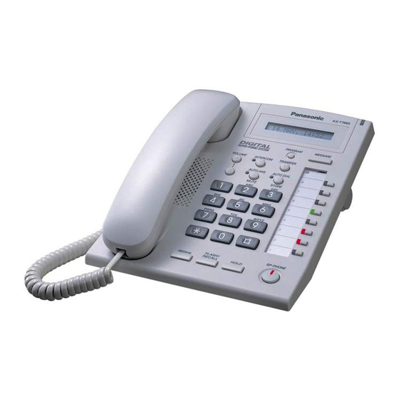
Digital Proprietary Telephone
KX-T7665AL
KX-T7665X
(for Australia, Asia, Middle Near East, Africa and Latin
America)
© 2003 Panasonic Communications Co., Ltd. All
rights
reserved.
distribution is a violation of law.
ORDER NO. KMS0307792C3
Unauthorized
copying
and
Advertisement
Table of Contents

Related Manuals for Panasonic KX-T7665AL


Summary of Contents for Panasonic KX-T7665AL
- Page 1 When this mark does appear please read and follow the special instructions described in this manual on the use of PbF and how it might be permissible to use Pb solder during service and repair work. © 2003 Panasonic Communications Co., Ltd. All rights reserved.
-
Page 2: Table Of Contents
KX-T7665AL / KX-T7665X CONTENTS Page Page 1 ABOUT LEAD FREE SOLDER (PbF: Pb free) 10.3. LED CIRCUIT 1.1. SUGGESTED PbF SOLDER 10.4. RESET CIRCUIT 1.2. HOW TO RECOGNIZE THAT Pb FREE SOLDER IS 10.5. POWER SUPPLY CIRCUIT USED 10.6. DATA COMMUNICATION 2 FOR SERVICE TECHNICIANS 10.7. -
Page 3: About Lead Free Solder (Pbf: Pb Free)
KX-T7665AL / KX-T7665X 1 ABOUT LEAD FREE SOLDER (PbF: Pb free) Note: In the information below, Pb, the symbol for lead in the periodic table of elements, will refer to standard solder or solder that contains lead. We will use PbF solder when discussing the lead free solder used in our manufacturing process which is made from Tin, (Sn), Silver, (Ag), and Copper, (Cu). -
Page 4: How To Recognize That Pb Free Solder Is Used
R200 R503 R518 C503 C510 C521 C205 C528 R513 R514 MIC2 C518 PSUP1439Z-A R504 C516 C504 R508 PSUP1439Z-B C511 R510 R511 C508 C513 R512 C509 C507 C514 C512 R509 R507 C519 C502 KX-T7665AL / KX-T7665X : MAIN BOARD Marked PbF... -
Page 5: For Service Technicians
KX-T7665AL / KX-T7665X 2 FOR SERVICE TECHNICIANS ICs and LSIs are vulnerable to static electricity. When repairing, the following precautions will help prevent recurring malfunctions. 1. Cover the plastic parts boxes with aluminum foil. 2. Ground the soldering irons. 3. Use a conductive mat on the worktable. -
Page 6: Connection
KX-T7665AL / KX-T7665X 5 CONNECTION Caution: The availability of D-XDP function depends on the software version of the connected Business Telephone System. Consult your dealer for more details about D-XDP. -
Page 7: Disassembly Instructions
KX-T7665AL / KX-T7665X 6 DISASSEMBLY INSTRUCTIONS 1. Remove the Stand. 2. Remove 5 Screws (A). 3. Remove the Cabinet Cover. 4. Remove the Connector from the Main Board. 5. Remove 2 Screws (A). 6. Remove the Main Board and the LCD from the Cabinet Body. -
Page 8: How To Replace A Flat Package Ic
KX-T7665AL / KX-T7665X 7 HOW TO REPLACE A FLAT PACKAGE IC 7.1. PREPARATION 7.3. REMOVING SOLDER FROM BETWEEN PINS · PbF (: Pb free) Solder · Soldering Iron 1. Add a small amount of solder to the bridged pins. Tip Temperature of 700°F ± 20°F (370°C ± 10°C) 2. -
Page 9: Troubleshooting Guide
KX-T7665AL / KX-T7665X 8 TROUBLESHOOTING GUIDE 8.1. NO OPERATION Note: Refer to (1)~(4) of WAVEFORM (P.34) for waveform. -
Page 10: Lcd Does Not Operate
KX-T7665AL / KX-T7665X 8.2. LCD DOES NOT OPERATE Note: Refer to (5) of WAVEFORM (P.34) for waveform. -
Page 11: Handset Does Not Work
KX-T7665AL / KX-T7665X 8.3. HANDSET DOES NOT WORK Receive Send Note: Refer to (6)~(7) of WAVEFORM (P.34) for waveform. -
Page 12: Speaker-Phone Trouble
KX-T7665AL / KX-T7665X 8.4. SPEAKER-PHONE TROUBLE Receive Send Note: Refer to (6)~(7) of WAVEFORM (P.34) for waveform. -
Page 13: Dxdp-Dpt Does Not Work
KX-T7665AL / KX-T7665X 8.5. DXDP-DPT DOES NOT WORK Note: Refer to (8) of WAVEFORM (P.34) for waveform. -
Page 14: Block Diagram
KX-T7665AL / KX-T7665X... -
Page 15: Circuit Operations
KX-T7665AL / KX-T7665X 10 CIRCUIT OPERATIONS 10.1. KEY INPUT CONTROL CIRCUIT The key data is under the matrix control by 20 to 23(KEYOUT) and 28 to 35(KEYIN) of IC6. The key information outputted from KEYOUT is inputted into KEYIN, when the key is pressed. -
Page 16: Lcd Control Circuit
KX-T7665AL / KX-T7665X 10.2. LCD CONTROL CIRCUIT The LCD data is output from pins 52 to 58 of IC6. LCD contrast adjustment is performed by the circuit composed of R603 and R604. The contrast is determined only by the voltage level between pin 2 and pin 3 of CN5. Higher potential makes the contrast high. -
Page 17: Led Circuit
KX-T7665AL / KX-T7665X 10.3. LED CIRCUIT The lighting of the LED is controlled by pin 14 to 18 (Row) and pin 8 to 13 (Colum) of IC2. The LED lights up in a dynamic lighting system. The duty ratio is 1/8 (ON time 1.5ms). -
Page 18: Reset Circuit
KX-T7665AL / KX-T7665X 10.4. RESET CIRCUIT Reset Signal is outputted from IC7 and inputted into IC2, IC3 and IC6 at the connection of TEL cord. 10.5. POWER SUPPLY CIRCUIT This circuit converts the voltage supplied from PBX into the power supply voltage of +3.3V by IC1 (Switching Regulator IC). -
Page 19: Data Communication
KX-T7665AL / KX-T7665X 10.6. DATA COMMUNICATION Function The data communication circuit serves the following functions: Information exchanger between PBX and proprietary telephone, key input information as well as data for the LED control, LCD control, voice data, etc. This information is continuously exchanged at all times. -
Page 20: Dxdp Communication
KX-T7665AL / KX-T7665X 10.7. DXDP COMMUNICATION Function This circuit performs the same communication as DXDP-compatible DPT and PBX communication connected with DXDP port. Circuit Operation The data to Slave DPT is outputted from pin 33 and 34 of IC2 and sent by Transistor Q2 and Q3. -
Page 21: Analog Circuit
KX-T7665AL / KX-T7665X 10.8. ANALOG CIRCUIT This circuit performs the setting of the call path/vol. adjustment in each call mode by IC4. The audio gain of each call is determined by download data from PBX. · IC2 sends each audio data to IC3 by PCM interface. - Page 22 KX-T7665AL / KX-T7665X...
-
Page 23: Ic Data
KX-T7665AL / KX-T7665X 11 IC DATA 11.1. IC2 I/O Setting Pull-up Contents of Control Remark Processing Built-in chip select Built-in Read Built-in Write WAITN Wait INTN Interrupt out CLM5 LED column 5 CLM4 LED column 4 CLM3 LED column 3... - Page 24 KX-T7665AL / KX-T7665X I/O Setting Pull-up Contents of Control Remark Processing DVRL Comp. Ref. Comp. Input DVRH Comp. Ref. DDX0 Tx DATA OUT0 DDX1 Tx DATA OUT1 PVRL Comp. Ref. Comp. Input PVRH Comp. Ref. PDX0 Tx DATA OUT0 PDX1...
-
Page 25: Ic6
KX-T7665AL / KX-T7665X 11.2. IC6 I/O Setting Pull-up Contents of Control Remark Processing not in use not in use OSC2 not in use OSC1 8.192MHz clock from IC2 TEST not in use Reset/ Reset input P20/IRQ4 CODEC chip select P21/SCK1... -
Page 26: Terminal Guide Of Ics, Transistors And Diodes
KX-T7665AL / KX-T7665X I/O Setting Pull-up Contents of Control Remark Processing Built-in ADR0 ADR1 ADR2 ADR3 ADR4 ADR5 EEPROM CLK EEPROM DATA LCD_D7 LCD_D6 LCD_D5 LCD_D4 LCD_E LCD_W LCD_RS register select LCD contrast 1 Cont.H:L Cont.M/L:High"Z" TONED DTMF/Tone Tone out... -
Page 27: Cabinet And Electrical Parts Location
KX-T7665AL / KX-T7665X 13 CABINET AND ELECTRICAL PARTS LOCATION... -
Page 28: Accessories And Packing Materials
KX-T7665AL / KX-T7665X 14 ACCESSORIES AND PACKING MATERIALS... -
Page 29: Replacement Parts List
KX-T7665AL / KX-T7665X 15 REPLACEMENT PARTS LIST 1. RTL (Retention Time Limited) Ref. Part No. Part Name & Description Remarks Note: PQAS57P03Z SPEAKER The marking (RTL) indicates that the Retention Time is PSJS02P15Z CONNECTOR, 2 PIN PSUS1026Z TORSION SPRING limited for this item. - Page 30 KX-T7665AL / KX-T7665X Ref. Part No. Part Name & Description Remarks Ref. Part No. Part Name & Description Remarks (TRANSISTORS) R112 ERJ3GEYJ562 5.6K PSVTUMS1NTR TRANSISTOR(SI) R113 ERJ3GEYJ682 6.8K B1HFCFA00008 TRANSISTOR(SI) R114 ERJ3GEYJ103 XP4601 TRANSISTOR(SI) R115 ERJ3GEYJ472 4.7K 2SC4081R TRANSISTOR(SI) R116...
-
Page 31: For The Schematic Diagram
KX-T7665AL / KX-T7665X Ref. Part No. Part Name & Description Remarks Ref. Part No. Part Name & Description Remarks R523 ERJ3GEYJ473 C403 ECUV1C104ZFV R524 ERJ3GEYJ473 C404 ECUV1H120JCV R525 ERJ3GEYJ473 C405 ECUV1H120JCV R526 ERJ3GEYJ473 C406 ECUV1H120JCV R527 ERJ3GEYJ100 C407 ECUV1C104ZFV R600 ERJ3GEYJ822 8.2K... -
Page 32: Schematic Diagram
SW30 Vout 1 (10) AT/ST AT/MT HOLD KOUT[2] SW11 SW15 SW19 SW23 SW27 SW31 V/DWN V/UP INCOM REDIAL KOUT[3] SW12 SW16 SW20 SW24 SW28 SW32 KIN[0] KIN[1] KIN[2] KIN[3] KIN[4] KIN[5] KIN[6] KX-T7665AL / KX-T7665X : MAIN BOARD (1/2) KIN[7]... - Page 33 ADR0 R310 R311 NROW2 INTERCOM NROW1 R307 INTN INTN R308 NROW0 (10) RSTN C407 Z0.1 R300 SCAN CLM5 R304 SCANE CLM4 R407 R301 WAITN CLM3 R305 TEST CLM2 R302 MMODE CLM1 R303 CLM0 KX-T7665AL / KX-T7665X : MAIN BOARD (2/2)
-
Page 34: Waveform
KX-T7665AL / KX-T7665X 18 WAVEFORM Pin42 of IC2 and Pin8 of IC6 Rest signal Pin42 of IC2 and Pin8 of IC6 Pin48 of IC2 16.384MHz Pin45 of IC2 8.196MHz... - Page 35 KX-T7665AL / KX-T7665X Pin36 of IC2 Communication waveform Pin4 to 7 of CN5 Communication waveform Pin3 and 6 of IC3 PCM interface waveform between IC3 and IC2...
- Page 36 KX-T7665AL / KX-T7665X Pin8 and 10 of IC4 PCM interface waveform between IC4 and IC3 Pin31 of IC2 Communication waveform...
-
Page 37: Printed Circuit Board (Main Board)
R503 R518 C503 C510 C521 C205 C528 R514 R513 MIC2 C518 PSUP1439Z-A R504 C516 C504 R508 C511 R510 R511 C508 C513 R512 C509 C507 C514 C512 R509 R507 C519 C502 R313 KX-T7665AL / KX-T7665X : MAIN BOARD : COMPONENT VIEW... -
Page 38: Bottom View
V/UP SW11 V/DWN AT/MT AT/ST SW16 SW15 SW14 SW20 SW19 SW18 SW13 SW17 SW24 SW23 SW22 SW21 SW25 SW28 SW27 SW26 PSUP1439Z-B SW32 SW30 SW31 REDIAL FLASH HOLD SW29 KX-T7665AL / KX-T7665X : MAIN BOARD : BOTTOM VIEW KXT7665AL KXT7665X...