
Related Manuals for LG RH4820W


Summary of Contents for LG RH4820W
- Page 1 HDD/DVD RECORDER SERVICE MANUAL MODEL : RH4820W (RH4820WVL) CAUTION BEFORE SERVICING THE UNIT, READ THE “SAFETY PRECAUTIONS” IN THIS MANUAL. APRIL, 2004 P/NO : 3829RHP022D Printed in Korea...
- Page 2 CONTENTS SECTION 1 ..SUMMARY SECTION 2 ..CABINET & MAIN CHASSIS SECTION 3 ..ELECTRICAL SECTION 4 ..REPLACEMENT PARTS LIST...
-
Page 3: Table Of Contents
SECTION 1 SUMMARY CONTENTS NEW FUNCTIONS OF HDD/DVD-RECORDER ..............1-2 PRODUCT SAFETY SERVICING GUIDELINES FOR VIDEO PRODUCTS ....1-3 SERVICING PRECAUTIONS ....................1-4 • General Servicing Precautions • Insulation Checking Prodedure • Electrostatically Sensitive Devices SERVICE INFORMATION FOR EEPROM IC SETTING .......... -
Page 4: New Functions Of Hdd/Dvd-Recorder
NEW FUNCTIONS OF HDD/DVD-RECORDER • SUMMARY OF PRODUCT - RECORDING FUNCTION OF DVD-RW AND DVD-R SPECIFICATIONS • DVD-RW: VIDEO MODE AND VR MODE RECORD AVAILABLE • DVD-R :VIDEO MODE RECORD AVAILABLE - RECORDING FUNCTION OF HDD • TIMESHIFT • HDD TO DVD DUBBING •... -
Page 5: Product Safety Servicing Guidelines For Video Products
When servicing this product, under no circumstances should the original design be modified or altered without permission from LG Electronics Corporation. All components should be replaced only with types identical to those in the original circuit and their physical location, wiring and lead dress must conform to original layout upon completion of repairs. -
Page 6: Servicing Precautions
SERVICING PRECAUTIONS CAUTION : Before servicing the HDD/DVD Recorder cov- Electrostatically Sensitive (ES) Devices ered by this service data and its supplements and addends, Some semiconductor (solid state) devices can be damaged read and follow the SAFETY PRECAUTIONS. NOTE : if easily by static electricity. -
Page 7: Service Information For Eeprom Ic Setting
SERVICE INFORMATION FOR EEPROM IC SETTING MICOM START OPTION CONFIRMATION MODE DETECT NEW EEPROM (OPTION EDIT SCREEN) Press the "CLEAR" key on the EEPROM ID CHECK Remote controller and the "CH - " key 2 BYTE(B3,248,249) one the Front Panel the same time, then it goes in to Tracking initial mode. -
Page 8: Specifications
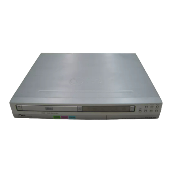
SPECIFICATIONS • GENERAL Power requirements AC 110-240V, 50/60 Hz Power consumption Dimensions (approx.) 430 X 69 X 377 mm (16.9 x 2.7 x 14.8 inches) (w x h x d) Mass (approx.) 6.4 kg (14.1 lbs) Operating temperature 5˚C to 35˚C (41˚F to 95˚F) Operating humidity 5 % to 90 % Television system... - Page 9 SECTION 2 CABINET & MAIN CHASSIS CONTENTS 1. EXPLODED VIEWS .......................2-2 1. Cabinet and Main Frame Section ..................2-2 2. Deck Mechanism Section(RL-01A) ..................2-3 3. Packing Accessory Section ....................2-4...
-
Page 10: Exploded Views
EXPLODED VIEWS 1. Cabinet and Main Frame Section... -
Page 11: Deck Mechanism Section(Rl-01A)
2. DECK MECHANISM SECTION(RL-01A) A01A 019A... -
Page 12: Packing Accessory Section
3. Packing Accessory Section OPTIONAL PART 810 CABLE ASS'Y 821 SCART CABLE 808 Battery Cable, Coaxial Remote Control Plug Ass'y, 1Way Instruction Ass'y Plug Ass'y, 2Way Packing Packing... - Page 13 SECTION 3 ELECTRICAL CONTENTS HDR PART RL-01A LOADER PART ELECTRICAL TROUBLESHOOTING GUIDE ..3-2 ELECTRICAL TROUBLESHOOTING GUIDE ..3-79 1. POWER ( SMPS ) CIRCUIT (PART 1) ..3-2 BLOCK DIAGRAMS &...
-
Page 14: Section
HDR PART ELECTRICAL TROUBLESHOOTING GUIDE 1. Power ( SMPS ) Circuit (Part 1) No VF+ No 5VD Is 5.2VA section working? Is 5.2VA section working? Is 5.2V present at Check R102 No 5.2VA emitter of Q120? Replace R102 Check F101 Replace Q120 Is there a DC voltage at Replace TH01... -
Page 15: Power ( Smps ) Circuit (Part 2)
2. Power ( SMPS ) Circuit (Part 2) No 1.8V No 3.3V Is 3.8VA section working? Is 3.8VA section working? Is there a DC voltage at Is there a DC voltage at No 3.8VA IC160 1PIN IC154 1PIN Is there a DC voltage Check IC160 Check IC154 D122(-)? -
Page 16: System Circuit
3. SYSTEM Circuit LG LOGO not displayed at POWER : ON. IC308 - 8 : HIGH? Check IC308 power and ( /E5_RST ) other circuits X101 : Clock oscillated? Replace X101 ( 13.5 MHz ) RESET IC202 - 26 : check... -
Page 17: When Playing Disc ,No Audio Output
5. When playing DISC ,no audio output IC702 - 46: HIGH ? Check IC702 power and ( LOW: AUDIO MUTE ) other circuits IC201 – 14,15,18,19 Check IC201 power and Check audio output other circuits IC201 - 1 : HIGH ? Check IC309 power and RESET_Audio status) other circuits... -
Page 18: No Tuner Audio Output
7. No TUNER audio output Audio output even when < When playing DISC , no Playing Disc audio output> check IC808,809 - 7 IC808,809 (AUDIO SWITCH) Power and switching operation Check audio signal output Pin 2,4 High/Low =>pin 7 output : SW_A_OUT_L/R IC808,809-3 Check IC808,809signal Check audio signal input... - Page 19 IC807 - 2 : Check SIF Check C866, TUNER signal input signal flow When changing a channel, IC702 - Check IC702 power and 69 : HIGH after RESET signal other circuits IC702 - 39 : Check IC705 power and No Sync signal input other circuits No TUNER VIDEO signal Check Q702 ( V.Buffer TR)
-
Page 20: No External Input 1 Audio
8. No external input 1 audio Audio output even when When playing DISC , no Playing Disc audio output> check IC808,809 - 7 IC808,809 (AUDIO SWITCH) Power and switching operation Check audio signal output Pin 2,4 High/Low =>pin 7 output : SW_A_OUT_L/R IC808,809-3 Check IC808,809signal Check audio signal input... -
Page 21: No External Input 2 Audio
9. No external input 2 audio Audio output even when When playing DISC , no Playing Disc audio output> check IC808, 809 - 7 IC808, 809 (AUDIO SWITCH) Power and switching operation Check audio signal output Pin 2, 4 High/Low =>pin 7 output : SW_A_OUT_L/R IC808, 809-3 Check IC808,809 signal Check audio signal input... -
Page 22: No External Input 3 Audio
10. No external input 3 audio Audio output even when When playing DISC , no Playing Disc audio output> check IC808,809 - 7 IC808,809 (AUDIO SWITCH) Power and switching operation Check audio signal output Pin 2,4 High =>pin 7 output : A1_L/R Pin 2,4 High/Low =>pin 7 output : TU_L/R IC808,809-5 Check JK801 Audio L/R... -
Page 23: No Rgb/ Component Video Signal When Playing Disc
12. No RGB/ Component video signal when playing DISC SW801 Q High? Check IC702 around Q808 Emitter High? IC702 - 49 : HIGH ? circuits Check IC702 – 85 : High input IC806 – 16, 18, 20 Check IC806 power and IC806 –... -
Page 24: No Composite/S-Video Signal When Playing Disc
13. No composite/S-Video signal when playing DISC No COMPOSIT signal? S-VIDEO: No Y signal? S-VIDEO : No C signal? IC804 – 29, 30 Check R810, C927 Check R804,C892 Check output IC806 – 21 IC806 – 26 Check R918, C925 Check output Check output IC806 –... -
Page 25: No Tv , External Input Video Signal
14. No TV , external input video signal No video signal of external input When connecting Tuner, No video signal of external 3/4Rear Composite/Front No TV video signal input 1/2(Rear Scart input) Composite ,S-video ) Check IC804 - 1,3(input) and Check Tuner power and JACK CABLE =>... -
Page 26: No Dv( Ieee 1394 ) Input (Video/Audio) Signal
15. No DV( IEEE 1394 ) input (video/audio) signal CheckDV_JACK and CABLE connection IC401 - 42,43,44,45 Check signal input IC401 - 78:HIGH? Check IC309-12 signal ( /RST_PHY ) Check IC401 - 2 Clock ? Check X402 Clock BIO_PHY_CLK 24.576 MHz IC401 =>... -
Page 27: Block Diagrams
BLOCK DIAGRAMS 1. Overall Block Diagram A1_In DDR SDRAM I/O B'd MAIN B'd 8M WordX4 N/A2 CVBS_Out I/O B'd MSP3417 S_VIDEO_Out V_ENC Y/Pb/Pr or R/G/B V0_D[0:15] ADV7302 ADV7302 A_ADC Tuner AI_D0 CS5340 CS534 Optical & Digital S/PDIF A0_IEC958 Audio Out S1 / S2 A0_D A_ADC:2ch... -
Page 28: In/Out Block Diagram
2. In/Out Block Diagram FRONT JACK FRONT JACK I/O JACK I/O U-COM A2 L/R IN V2 IN Y/C IN C_SYNC_IN V1 IN A1 L/R IN MM1109 TUNER TU_V_OUT SDA5650 MM1510 Sync AUDIO SEL 1,2 NJM2521 6dB Buffer Seperator AUDIO SWICH TU A OUT Audio_Sel_1 Buffer... -
Page 29: Video Block Diagram
3. Video Block Diagram SCL/SDA TU_Vz_IN VI_D[0:7] Y_IN VI_CLK C_IN IC501 VI_VSYNCO V1_IN SAA7115 V2_IN VIDEO Decoder 24.576MHz IC101 /RST_7115 DMN8650 SCL/SDA VO_D[0:15] IC502 VO_CLK CVBS ADV7302 VIDEO R / Pr Encoder G / Y B / Pb /RST_7302 3-19 3-20... -
Page 30: Video Sw Path Block Diagram
4. Video SW Path Block Diagram AV4/S-V V1_IN PB_IN V.DEC TU_V_OUT IC806 CVBS_OUT MM1623 (6dB A.) SW_V_OUT(TU/E1/E2) IC805 IC811 MM1510 SDA5650 (6dB,75 ) (VPS) V.ENC IC706 IC705 IC702 MM1510 MM1109 (u-COM) (6dB,75 ) (Sync SEP.) 3-21 3-22... -
Page 31: Audio Block Diagram
5. Audio Block Diagram A1/A2_L_IN IC808,809 IC803 AI_DO FRONT/REAR AUDIO S/W IC815 OP AMP JACK NJM2521 CS5340 A1/A2_R_IN MC33202 AI_SCLK AUDIO AI_FSYNC SW_A_OUT L/R ADC_MCLK TU_A_L MSP3417 MPEG AUDIO PROCESSOR TU__A_R IC804 EU1_A_IN_L AO_SCLK MM1443 AV SWITCH AO_FSYNC L - OUT EU1_A_IN_R IC201 IC810... -
Page 32: Audio Sw Path Block Diagram
6. Audio SW Path Block Diagram 26(22) 8(14) 10(16) 25(21) IC807 30(31) 24(20) SW4(1) MSP3417 27(23) (NICAM/A2) SW5(2) 1(7) 6(12) IC810 SW6(3) NJM5532 (OP AMP) IC804 3,2(5,6) 18,19(14,15) IC201 IC815 10(12) 1(7) IC803 IC808(809) CS5340 CS4392 2(6) MC33202 NJM2521 (ADC) (DAC) (OP AMP.) (SW w/Buffer) -
Page 33: Fld / Μ-Com Block Diagram
7. FLD / µ-COM Block Diagram X704 18.432MHz AV S/W TU_L/R_IN IC804 Multi Sound MM1443 IC807 MSP3417 ITL_RESET_L X901 EEPROM 10MHz X702 X701 TUNER IC701 10MHz 32.768MHz TU801 AT24C16 G( ) FLD_TXD MICOM I2C_DATA,CLK IC501 BJ879GNK P( ) PD780232 Sync. Sep. AV S/W. -
Page 34: Power : Main Board Block Diagram
8. Power : Main Board Block Diagram 3.3V 3.3VA 2.5V 1.9V FLASH 74ALVT16373 74ALVT16373 74ABT245 74ABT245 DMN8650 74LVC04 3.3V E5_VPAD 74LVC04 74ABT541 74ABT541 3.3V E5_AVDD 3.3V E5_VDDX 74LVC08 74LVC08 3.3V E5_VDDREF AD8061 AD8061 1.9V E5_VCORE EPM3032A EPM3032A SSTL2_VDD 2.5V 74LVC827 74LVC827 1.25V MBM29DL640E... -
Page 35: Power : I/O Board Block Diagram
9. Power : I/O Board Block Diagram 12VA 33VT U-COM DAC_Analog Cync. SEP V.SW (C+) Nicam/A2 Tuner (H8S-2196) (CS4392) (MM1109) (MM1443) (MSP3417) Reset IC Diff OP AMP V.S/W (KIA7031P) (NJN5532) (MM1623) PWR Fail A.SW (KIA7042) (NJM2521) Optical Drive EEPROM (AT24C16) 5VAA Audio DAC VPS/PDC... -
Page 36: Layout Connection Block Diagram
10. Layout Connection Block Diagram Optical S1/S2 AV1/S/Comp/Digital Input/Output Board DownLoad 12VA Video Audio& 33VT CN101 CN502 1.9V 2.5V 3.3V 5.1V CN601 SMPS Board J602 Main Board UART1 ATAPI DVD + RW DRIVER J301 CN602 J603 CN501 MEMORY DV_in CARD S/Jack Jack Board... -
Page 37: Smps Block Diagram (Part 1)
11. SMPS Block Diagram (PART 1) TIMER H RECTIFIER(FLD) -29VA REG(12V) AUDIO RECTIFIER(14V) 12VT REG(12V) / 12VA TUNER REG(2.5V) 2.5V RECTIFIER(3.2V) / 1.5V REG(1.5V) MAIN 33VT RECTIFIER(35V) TUNER 5.2VA FRONT RECTIFIER(5.2V) 5VT/5VA TUNER FEED B. AC85~240V PWR CTL 3-35 3-36... -
Page 38: Smps Block Diagram (Part 2)
12. SMPS Block Diagram (PART 2) RECTIFIER(14V) REG(12V) LOADER RECTIFIER(5.8V) REG(12V) LOADER 1.8V RECTIFIER(2.3V) REG(1.8V) MAIN 3.3V RECTIFIER(3.7V) REG(3.3V) MAIN FEED B. AC85~240V PWR CTL 3-37 3-38... -
Page 39: Circuit Diagrams
CIRCUIT DIAGRAMS 1. POWER CIRCUIT DIAGRAM VF(+) Power dead 12V Power dead R107 is defective IC153 is defective 2.5V Power dead IC159 is defective 12VT or 12VA Power dead IC153 is defective Power dead IC101 is defective 5VD Power dead Q120 and Q121 is defective Power dead 33V Power dead... -
Page 40: E5 Bga, Power, Uart2 Circuit Diagram
2. E5 BGA, POWER, UART2 CIRCUIT DIAGRAM E5 BAG, POWER, UART2 3-41 3-42... -
Page 41: Ddr Sdram, Flash Circuit Diagram
3. DDR SDRAM, FLASH CIRCUIT DIAGRAM HY5DU281622DT-6 HY5DU281622DT-6 HY5DU281622DT-6 HY5DU281622DT-6 DDR SDRAM, FLASH 3-43 3-44... -
Page 42: Rst, Control/Status Reg, Atapi, Host Cpld, Latch Circuit Diagram
4. RST, CONTROL/STATUS REG, ATAPI, HOST CPLD, LATCH CIRCUIT DIAGRAM RST, CONTROL/STATUS REG, ATAPI, HOST CPLD, LATCH 3-45 3-46... -
Page 43: 4, Ethernet Connector Circuit Diagram
5. 1394, ETHERNET CONNECTOR CIRCUIT DIAGRAM 1394, ETHERNET CONNECTOR 3-47 3-48... -
Page 44: Video In/Out Circuit Diagram
6. VIDEO IN/OUT CIRCUIT DIAGRAM VIDEO IN/OUT 3-49 3-50... -
Page 45: Audio In/Out Circuit Diagram
7. AUDIO IN/OUT CIRCUIT DIAGRAM AUDIO IN/OUT 3-51 3-52... -
Page 46: I/O Micom Circuit Diagram
8. I/O MICOM CIRCUIT DIAGRAM SR17208A I/O MICOM 3-53 3-54... -
Page 47: Tuner, Video In/Out Circuit Diagram
9. TUNER, VIDEO IN/OUT CIRCUIT DIAGRAM 3.9K 3.9K SR17209A TUNER, VIDEO IN/OUT 3-55 3-56... -
Page 48: Front Circuit Diagram
10. FRONT CIRCUIT DIAGRAM HDD+VDR_FRONT 3-57 3-58... -
Page 49: Onspec 3 In 1 Memory Card & Dv Avin Circuit Diagram
11. Onspec 3 In 1 Memory Card & DV AVIN CIRCUIT DIAGRAM L909 A GND L910 A GND A GND A GND A GND A GND A GND A GND A GND A GND A GND A GND Onspec 3 In 1 Memory Card & DV AVIN 3-59 3-60... -
Page 50: Waveforms
• WAVEFORMS X101 IC501 IC501 CN601 CN601 IC206 IC401 13.5MHz PIN32 PIN31 PIN24 PIN26 PIN45 PIN77 HOST_RXD HOST_TXD SDRAM_SCLK0 24.576MHz IC401 IC501 IC501 IC501 CN502 CN502 CN502 PIN2 PIN94 PIN91 PIN6 PIN6 PIN4 PIN2 BIO_PHY_CLK VI_CLK0 VI_SYNC0 24.576MHz CVBS_OUT Y_OUT C_OUT CN502 CN502... -
Page 51: Circuit Voltage Chart
• CIRCUIT VOLTAGE CHART MODE MODE MODE MODE MODE MODE MODE PIN NO. PIN NO. PIN NO. PIN NO. PIN NO. PIN NO. PIN NO. IC202 2.49 2.49 0.02 0.02 0.02 3.25 3.25 3.25 1.33 1.33 1.33 1.25 1.24 0.24 0.03 0.03 0.03... - Page 52 MODE MODE MODE MODE MODE MODE MODE PIN NO. PIN NO. PIN NO. PIN NO. PIN NO. PIN NO. PIN NO. 2.38 2.38 2.38 4.35 4.35 4.35 5.08 2.06 2.06 2.06 5.75 5.74 5.74 IC807 IC815 2.38 2.38 2.38 11.64 11.64 5.08 5.07...
- Page 53 MODE PIN NO. Q120 Q121 5.02 Q122 Q123 32.7 32.6 Q124 3-67 3-68...
-
Page 54: Printed Circuit Diagrams
PRINTED CIRCUIT DIAGRAMS 1. MAIN P.C.BOARD(TOP SIDE) LOCATION GUIDE 3-69 3-70... -
Page 55: Main P.c.board(Bottom Side)
2. MAIN P.C.BOARD(BOTTOM SIDE) LOCATION GUIDE 3-71 3-72... -
Page 56: I/O P.c.board
3. I/O P.C.BOARD LOCATION GUIDE LOCATION GUIDE 4. JACK P.C.BOARD LOCATION GUIDE LOCATION GUIDE 3-73 3-74... -
Page 57: Front P.c.board
5. FRONT P.C.BOARD 6. KEY P.C.BOARD LOCATION GUIDE 3-75 3-76... -
Page 58: Power P.c.board
7. POWER P.C.BOARD LOCATION GUIDE 3-77 3-78... -
Page 59: Rl-01A Loader Part
RL-01A LOADER PART ELECTRICAL TROUBLESHOOTING GUIDE Reset or Power Check. Check it after connecting the power cable only for NO Reset or Power ON. •Check the power(5V,12V)short. Are the pin 41, 44 of CN201 •Check the PC power cable. +12V, +5V respectively after the power •Repair the PC power supply. - Page 60 System Check Load tray without inserting disc. Does tray operate normally? Go to “Tray operating is abnormal” Does pick-up move to inside? Go to “Sled operating is abnormal” Go to “Focus Actuator operating is Does pick-up lens move abnormal” up/down? Does laser turn on? Go to “Laser operating is abnormal”...
- Page 61 Tray operating is abnormal Tray open doesn ’t work. Is the Input voltage 0V at IC302 •Check the connection of IC302 pin 60. pin 60 when push the •Replace the EJECT SW. EJECT SW? •Check the connection of IC103 pin 19. Is there tray •Replace the IC103.
- Page 62 Sled operating is abnormal Is there sled control signal output? Replace the IC103 (IC103 pin 8,9) Is there •Check the connection of IC105 pin 28,29. sled drive signal input? •Replace the IC105. (IC105 pin 28,29) •Check the R132,R133. Is there Is DRV-CTRL1 sled drive voltage output? signal “H”?
- Page 63 Spindle operating is abnormal Is there Is there spindle control DSP spindle control signal input? output(IC202 pin 145)? (IC105 pin 24) •Check the R147,R149. •Replace the IC106 Replace the IC202. Is there Is there spindle drive voltage output? SFG signal input? (IC105 pin 9,11,18) (IC302 pin 28) Replace the Spindle Motor...
- Page 64 Focus Servo is unstable Is FE signal output normal in Focusing Replace the IC107. Up/Down? (IC107 pin 86) Is FDRV signal output normal in Focusing •Check the R158. Up/Down? •Replace the IC107. (IC202 pin 146) Go to “Focus Actuator operating is abnormal” Focus Actuator operating is abnormal.
- Page 65 Track Servo is unstable Is TE signal Is pick-up output normal in focusing (E, F, G, H)output normal? ON and tracking OFF? (CN101 pin 5, 8, 9, 12) (IC107 pin 82) Replace the IC107. •Check the pick-up FFC. •Replace the pick-up. Is TE signal input normal in focusing Check the connection between...
- Page 66 Recognition Fail Case 1: CD-ROM Fail Check pick-up read power Go to “LD CHECK”. is 0.9~1.3mW? Does focus servo Go to “Focus Servo is unstable”. operate normally? Check pick-up RF signal IC107(Pin115) •Check the pick-up FFC and CN101. RFO(TP115)is •Replace the pick-up unit. 500~1000mVpp? Check RFEQO waveform Replace the IC107...
- Page 67 Recognition Fail Case 2:DVD Fail Check pick-up read power Go to “LD CHECK”. was 0.9~1.1mW? Is IC302 pin 46(LDEN-DVD)level Replace the IC302. was about 3.3V? Is there RF signal at CN101 Replace the pick-up. pin 13,14. Is there RF signal Replace the IC107 at IC107 pin 99.
- Page 68 LD CHECK (Laser operating is abnormal) Execute “B.Check ALPC Parameters” of “How to use Test Tool” Execute “C.Laser Power Setup”of Is ALPC parameters “How to use Test Tool” valid? Execute “D.Laser Inspection” of “How to use Test Tool” Check reference voltage. OFF level VRDC level &FPD VWDC1 level &FPD...
- Page 69 CD/DVD ? Execute “E.ALPC Test for AS”of “How Execute “E.ALPC Test for AS”of “How to Test Tool”(Select “DVD VRDC Loop” to Test Tool”(Select “CD VRDC Loop” and trigger) and trigger) Check the input of LDEN-CD. Check the input of LDEN-DVD. (pin 33 of CN101 :‘H ’) (pin 17 of CN101 :‘H ’) Check the input of VRDC.
- Page 70 Execute “E.ALPC Test for AS”of “How Execute “E.ALPC Test for AS”of “How to Test Tool”(Select “DVD-R Rec to Test Tool”(Select “DVD-RW Rec Mode”and trigger) Mode”and trigger) Check the input of LDEN-DVD. Check the input of LDEN-DVD. (pin 17 of CN101 : ‘H’) (pin 17 of CN101 : ‘H’) Check the input of VWDC.
- Page 71 …? change it. Is the write tool supported by Use LG bundle software. LG Drive? Check disc information on writing tool. [If you get some data information with “Non Recordable Disc ”message,the...
- Page 72 Writing Part Check Load tray with DVD ±R/RW disc. Run and write with writing tool. Does the Do the IC302 blink of LED1,LED2 occurs pin 58,59 output toggle during writing? signals during writing? • Check the connection between IC302 pin 58,59 and LED. •...
-
Page 73: Block Diagrams & Description
BLOCK DIAGRAMS & DESCRIPTION 1. Overall Block Diagram 3-93... -
Page 74: Major Ic Internal Block Diagram And Pin Description
2. MAJOR IC INTERNAL BLOCK DIAGRAM AND PIN DESCRIPTION IC101 (µPC3320) : RF Signal Processor for CD/DVD Pin Assignment GND0 RECD SWRF1 SWRF2 MONI3 GND7 GND1 SPP2 SBAD PPALL VCC2 TECIN µPC3320 REFI2 REFO1 VCC7 RF IC MONI2 WOBBLE CWHP GND2 CWAGC VCC33... -
Page 75: Block Diagram
Block Diagram EQCK1 WLDM EQCK2 WREF SCFCK RLDM PELD P2LD ROPC1 ROPC2 HPAD HPBC WRF2 WRFLP SWRF1 SWRF2 CWAGC CWHP CDPDRF CDPDA CDPDB CDPDC CDPDD ADIN BCIN AGCIN RCBH1A RCBH1B MONI 3PIN CEQOS1 CEQOS2 3-95... - Page 76 Pin description Pin Name Type Description GND0 Analog GND SWRF1 OUTPUT WRF signal sampling & hold [S/H] signal output. SWRF1 OUTPUT WRF signal sampling & hold [S/H] signal output. INPUT RF differerential signal[+] input. INPUT RF differerential signal[-] input. GND1 Analog GND INPUT Main beam signal [A1] input.
- Page 77 Pin Name Type Description VCC4 Analog power. OUTPUT Wobble circuit [A+D] signal output. OUTPUT Wobble circuit [B+C] signal output. GND4 Analog GND CDAC OUTPUT DAC reference voltage output. VCC5 Digital power. BCIN INPUT [B+C] signal input. ADIN INPUT [A+D] signal input. RCBH1A RLPP circuit bottom hold condenser connecting port.
- Page 78 Pin Name Type Description OUTPUT Tracking error signal output. OUTPUT Tracking error signal output for Servo. PPALL OUTPUT Main side push-pull signal output. SBAD OUTPUT Sub beam signal output [ (E+F+G+H) signal]. SPP2 Sub beam signal output [ (F+G)-(E+H) signal]. OUTPUT Focus error signal.
-
Page 79: Major Ic Internal Block Diagram And Pin Description
3. MAJOR IC INTERNAL BLOCK DIAGRAM AND PIN DESCRIPTION IC201(µPD63620) : Encoder, Decoder & DSP Signal Processor Pin Assignment DGND PULLUP DASP HCS1 HCS0 HDA2 HDAD PDI AG DVDD33 HDA1 HIOCS16 HINTRQ SLED DVDD33 DGND DVDD25 HDMACK REFOUT IORDY SDRV DIOR TDRV DIOW... - Page 80 Block Diagram 3-100...
- Page 81 Pin description Pin No. Pin Name Type Description DGND Digital GND PULLUP Pull-up resistance connecting port.[5V or 3.3V] DASO 5V_tolerant Pull-up Drive active slave presesnt signal.[open/drain] HCS1 5V_tolerant Host interface chip, pull-up selection input. HCS0 5V_tolerant Host interface chip, pull-up selection input. HDA2 5V_tolerant Host interface chip, address signal input.
- Page 82 Pin No. Pin Name Type Description DGND 5V_tolerant Pull-up Host interface data bus.[within slave resistance HDD4 HDD3 5V_tolerant Pull-up Host interface data bus.[within slave resistance] HDD3 HDD11 5V_tolerant Pull-up Host interface data bus.[within slave resistance] HDD12 HDD4 5V_tolerant Pull-up Host interface data bus.[within slave resistance HDD2 HDD7 5V_tolerant...
- Page 83 Pin No. Pin Name Type Description DGND Digital GND.(Buffer. Memory. Block) MD13 Pull-up Buffer memory , Interface data bus. Pull-up Buffer memory , Interface data bus. MD12 Pull-up Buffer memory , Interface data bus. Pull-up Buffer memory , Interface data bus. DGND Digital GND.
- Page 84 Pin No. Pin Name Type Description DGND Buffer memory , Interface data bus. Buffer memory , Interface data bus. Buffer memory , Interface data bus. Buffer memory , Interface data bus. Buffer memory , Interface data bus. DGND Digital GND Buffer memory , Interface data bus Buffer memory , Interface data bus.
- Page 85 Pin No. Pin Name Type Description MIRRBCA Pull-up RF AMP PC3320 RF equalizer automatic follow-up clock output. EQCK1 Pull-up RF AMP PC3320 RF equalizer fixed clock output. SCFCK RF AMP PC3320 RF equalizer automatic follow-up clock output. WLDON Laser, Driver write laser control signal. ROPC2 Running OPC,sample hold signal.
- Page 86 Pin No. Pin Name Type Description 5V_tolerant Access control signal output from Local CPU to SDRAM. DVDD33 Digital power[3.3V] 5V_tolerant Local CPU Adress bus. 5V_tolerant Local CPU Adress bus. 5V_tolerant Local CPU Adress bus. 5V_tolerant Local CPU Adress bus. 5V_tolerant Local CPU Adress bus.
- Page 87 Pin No. Pin Name Type Description DVDD33 Digital power[3.3V] EFPULSE OFF pluse output[write laser/driver control signal]. PKPULSE1 Peak pluse output[write laser/driver control signal]. PKPULSE2 Peak pluse output[write laser/driver control signal]. HDDREV Host interface data bus selector.[H: general, L: reverse] AGND Analog GND[WWAPLL] AVDD Analog power 2.5V [WWAPLL]...
-
Page 88: Ic302(Upd76F0047):Micom
4. IC302(uPD76f0047):MICOM Pin Assignment 3-108... - Page 89 Block Diagram INTC INTP0-INTP7 Instruction Flash queue 768KB TIP00-TIP50 32bit Timer/Counter CS0 - CS3 barrel Multipuller TIP01-TIP51 (16bit Timer) shifter (16 x 16 -> 32) AD0-AD15 x 6ch A0 - A21 System TOP01-TOP51 24KB register WR0-WR1 Interval Timer General ASTB (16bit Timer) register WAIT...
- Page 90 Pin description Pin No. Pin Name Type Des cription AVREF0 A/D CONVERTER REFERENCE VOLTAGE INPUT AVSS A/D,D/A CONVERTER POTENTIAL STEP0 STEPPTING MOTOR CONTROL SIGNAL STEP1 STEPPTING MOTOR CONTROL SIGNAL AVREF1 D/A CONVERTER REFERENCE VOLTAGE INPUT TILT-MUTE TILT DRIVE MUTE SIGNAL SBRK EXTERNAL MEMORY ADDRESS BUS FLMD0...
- Page 91 Pin No. Pin Name Type Des cription REGISTER ADDRESS OUPUT /DACS CHIP SELECTOR /BPRCS EEPROM COMM UNICATON LINE TEST MOD0 TEST MOD1 (RESERVED) (RESERVED) LED ENABLE LINE LED ENABLE LINE /EJECT-KEY TRAY OPE N LINE URDY ACCESS CONTROL SIGNAL INPUT FRON CPU TO SDRAM (RESERVED) /OPEN-SW OPEN S/W INPUT...
-
Page 92: Waveforms
WAVEFORMS 1. POWER & RESET Signal 12 V(CN201 PIN41) 5 V(CN201 PIN 44) /HRST(IC203 PIN 3) /RST(IC203 PIN2) POWER IN 2. Main Clock1 for IC202 (16.9MHz) 12 V(CN201 PIN41) 5 V(CN201 PIN 44) /HRST(IC203 PIN 3) /RST(IC203 PIN2) POWER IN 3-112... -
Page 93: Main Clock2 For Ic302 (20Mhz)
3. Main Clock2 for IC302 (20MHz) X301(IC302 PIN 13 GND LEVEL 4. SDRAM Clock MCLK(IC201 PIN 35) GND LEVEL 3-113... -
Page 94: Tray Open/Close Signal 1
5. TRAY OPEN/CLOSE SIGNAL 1 /EJECT-KEY (SW 302 PIN1) TRAY-CTRL(REF 1.25V) 8.4V 5.8V (IC105 PIN26) TRAY+(CN104 PIN 1) 8.4V 5.8V TRAY-(CN104 PIN 2) OPEN CLOSE 6. TRAY OPEN/CLOSE SIGNAL 2 /EJECT-KEY (SW 302 PIN1) TRAY-CTRL (IC105 PIN26) /OPEN-SW (SW301 PIN 2) /LOAD-SW (SW301 PIN 1) OPEN... -
Page 95: Sled Move Signal 1
7. SLED MOVE SIGNAL 1 1.7V 1.25V 0.9V STEP0 1.6V 1.25V (IC103 PIN8) 0.9V STEP1 (IC103 PIN9) A+(CN102 PIN 2) A-CN102 PIN 3) ZOOM 8. SLED MOVE SIGNAL 2 STEP0 (IC103 PIN8) STEP1 (IC103 PIN9) A+(CN102 PIN 2) A-CN102 PIN 3) 3-115... -
Page 96: Focus Search Signal
9. FOCUS SEARCH SIGNAL FDRV(REF 1.25V) (IC105 PIN53) F+(REF 2.5V) (CN101 PIN 35) F-(REF 2.5V) (CN101 PIN 36) 10. LASER TURN ON SIGNAL F+(REF 2.5V) (CN101 PIN 35) LDEN-DVD(CN101 PIN17) VRDC(CN101 PIN 27) 3-116... -
Page 97: Disc Type Judgement Waveform (Cd Series)
11. DISC TYPE JUDGEMENT WAVEFORM (CD SERIES) F+(REF 2.5V) (CN101 PIN 35) FE(REF 1.5V) (IC107 PIN86) ZOOM 12. DISC TYPE JUDGEMENT WAVEFORM (CD&CD-R) F+(REF 2.5V) (CN101 PIN 35) FE(REF 1.5V) (IC107 PIN86) 3-117... -
Page 98: Disc Type Judgement Waveform (Cd-Rw)
13. DISC TYPE JUDGEMENT WAVEFORM (CD-RW) F+(REF 2.5V) (CN101 PIN 35) FE(REF 1.5V) (IC107 PIN86) 14. DISC TYPE JUDGEMENT WAVEFORM (DVD SERIES) F+(REF 2.5V) (CN101 PIN 35) FE(REF 1.5V) (IC107 PIN86) ZOOM 3-118... -
Page 99: Disc Type Judgement Waveform (Dvd_Single&R)
15. DISC TYPE JUDGEMENT WAVEFORM (DVD_SINGLE&R) F+(REF 2.5V) (CN101 PIN 35) FE(REF 1.5V) (IC107 PIN86) 16. DISC TYPE JUDGEMENT WAVEFORM (DVD _DUAL) F+(REF 2.5V) (CN101 PIN 35) FE(REF 1.5V) (IC107 PIN86) 3-119... -
Page 100: Disc Type Judgement Waveform (Dvdrw)
17. DISC TYPE JUDGEMENT WAVEFORM (DVDRW) F+(REF 2.5V) (CN101 PIN 35) FE(REF 1.5V) (IC107 PIN86) 18. SPINDLE WAVEFORM1 2.25V 1.25V SPIN (REF 1.25V) (IC105 PIN 24) 1.25V SRVC (REF 1.25V) (IC105 PIN 27) SFG(IC105 PIN21) 3-120... -
Page 101: Spindle Waveform2
19. SPINDLE WAVEFORM2 U(IC105 PIN9) V(IC105 PIN11) W(IC105 PIN18) W(IC105 PIN18) 20. FOCUS ON SIGNAL(CD) F+(REF 2.5V) (CN101 PIN 35) FE(REF 1.5V) (IC107 PIN86) T+(REF 2.5V) (CN101 PIN 37) TE(REF 1.5V) (IC107 PIN82) ZOOM 3-121... -
Page 102: Focus On Signal(Dvd)
21. FOCUS ON SIGNAL(CD) F+(REF 2.5V) (CN101 PIN 35) FE(REF 1.5V) (IC107 PIN86) T+(REF 2.5V) (CN101 PIN 37) TE(REF 1.5V) (IC107 PIN82) 22. FOCUS ON SIGNAL(DVD) F+(REF 2.5V) (CN101 PIN 35) FE(REF 1.5V) (IC107 PIN86) T+(REF 2.5V) (CN101 PIN 37) TE(REF 1.5V) (IC107 PIN82) ZOOM... -
Page 103: Focus On Signal (Dvd)
23. FOCUS ON SIGNAL (DVD) F+(REF 2.5V) (CN101 PIN 35) FE(REF 1.5V) (IC107 PIN86) T+(REF 2.5V) (CN101 PIN 37) TE(REF 1.5V) (IC107 PIN82) 24. TRACK OFF SIGNAL(CD) TE(REF 1.5V) (IC107 PIN82) TZC(IC107 PIN79) MIRRBCA (IC107 PIN92) 3-123... -
Page 104: Track Off Signal(Dvd)
25. TRACK OFF SIGNAL(DVD) TE(REF 1.5V) (IC107 PIN82) TZC(IC107 PIN79) MIRRBCA (IC107 PIN92) 26. Tilt Driver signal(Disc reading) 1.32V TILTDRV(IC104 PIN4) 1.25V 2.3V 2.35V TILT+(CN101 PIN39) 2.3V 2.25V TILT-(CN101 PIN40) 3-124... -
Page 105: Rf Waveform(Dvd)
27. RF WAVEFORM(DVD) 1.9V RFP(CN101 PIN13) 1.5V 2.5V RFO(IC107 PIN 115) 0.8V 2.0V RFI(IC107 PIN 99) 1.0V 28. RF WAVEFORM(CD) 2.30V RFP(CN101 PIN13) 1.65V 1.95V RFO(IC107 PIN 115) 1.15V 1.85V RFI(IC107 PIN 99) 1.05V 3-125... -
Page 106: Wobble(Dvd-R/Rw)_Reading
29. WOBBLE(DVD-R/RW)_READING AWOBBLE(IC107 PIN76) WOBBLE(IC107 PIN 75) 30. WOBBLE(DVD+R/RW)_READING&WRITING =>X1 SPEED AWOBBLE(IC107 PIN76) WOBBLE(IC107 PIN 75) 3-126... -
Page 107: Ld Enable(Dvd)
31. LD Enable(DVD) 3.3V LDENDVD(CN101 PIN 17) 3.3V LDENCD(CN101 PIN 33) 32. LD Enable(CD) LDENDVD(CN101 PIN 17) 3.3V LDENCD(CN101 PIN 33) 3.3V 3-127... -
Page 108: Laser Power(Reading)_Dvd+Rw
33. Laser Power(reading)_DVD+RW VRDC(IC107 PIN 31) About 360mv VWDC1(IC107 PIN 34) VWDC2(IC107 PIN 36) OPECTRG(IC107 PIN 55) 34. Laser Power(Erase)_DVD+RW VRDC(IC107 PIN 31) About 440mv VWDC1(IC107 PIN 34) VWDC2(IC107 PIN 36) OPECTRG(IC107 PIN 55) 3-128... -
Page 109: Laser Power(Writing)_Initial State
35. Laser Power(Writing)_initial state VRDC(IC107 PIN 31) 340m VWDC1(IC107 PIN 34) About 440mv VWDC2(IC107 PIN 36) OPECTRG(IC107 PIN 55) 36. Laser Power(Writing)_Processing VRDC(IC107 PIN 31) VWDC1(IC107 PIN 34) VWDC2(IC107 PIN 36) 3-129... -
Page 111: Circuit Diagrams
CIRCUIT DIAGRAMS 1. RF CIRCUIT DIAGRAM Title-drv is not good. (Level-shift IC) PD Gai Control IC (DRIVE IC) Focus & Spindle & Tracking is not good(Op-Amp) No sled & No Title (DA-converter) Analog-Switch Rd/Wr Toggle) SPINDLE DVD IR/RW(Blank Disc Recognition) SLED LASER POWER(ALPC) TRACKING... -
Page 112: Dsp Circuit Diagram
2. DSP CIRCUIT DIAGRAM (RESET IC) (SDRAM) (DSP IC) No Power, No operation 3-132 3-133... -
Page 113: Μ-Com Circuit Diagram
3. µ-COM CIRCUIT DIAGRAM Voltage Error Voltage Error EEPRON 1) Sled & filt drive is not good 2) Laser power drive is not good 3) Loader operation drive is not good (µ-COM) 3-134 3-135... -
Page 114: Printed Circuit Diagrams
PRINTED CIRCUIT DIAGRAMS 1. MAIN P.C.BOARD LOCATION GUIDE 3-136 3-137... - Page 115 1 WAY COAXIAL DT_HY_HIT_SEIL 1 6850R-PBA8H CABLE,COAXIAL 2 WAY COAXIAL RED_WHITE DT_HY *** REMOTE CONTROLLER 6711R1P071C REMOTE CONTROLLER ASSEMBLY H3 RH4820WVL LG W/O TV/DVD *** PANEL ASSEMBLY , FRONT,TIMER,KEY *** 3501R-2996L BOARD ASSEMBLY DVD RH4820WVL AA3SCL FRONT A43A 3721R-F814L PANEL ASSEMBLY,FRONT...
- Page 116 S AL LOCA. NO. PART NO. DESCRIPTION SPECIFICATION REMARKS C518 0CS225HJ6DC CAPACITOR,FIXED TANTALUM 2.2UF 3528 35V 20% SMD R/TP(SM C523 0CS225HJ6DC CAPACITOR,FIXED TANTALUM 2.2UF 3528 35V 20% SMD R/TP(SM C524 0CS225HJ6DC CAPACITOR,FIXED TANTALUM 2.2UF 3528 35V 20% SMD R/TP(SM D501 0DS121009AA DIODE,SWITCHING KDS121 TP KEC UMT 85V 300MA 2A...
- Page 117 S AL LOCA. NO. PART NO. DESCRIPTION SPECIFICATION REMARKS SW511 556-219B SWITCH,TACT THVV502GAA POSTECH DC 12 V 5- SW514 556-219B SWITCH,TACT THVV502GAA POSTECH DC 12 V 5- X501 6202R-BJ01A RESONATOR,CRYSTAL HC-49/S SUNNY 5.0000MHZ 30PPM ZD501 0DZ026809CA DIODE,ZENERS Z02W6.8V TP KEC SOT23 20W 6.8V ZD502 0DZ026809CA DIODE,ZENERS...
- Page 118 S AL LOCA. NO. PART NO. DESCRIPTION SPECIFICATION REMARKS 4930H-1092A HOLDER SHAFT GCC-4120B , 4370H-1079A SHAFT P/U(R/CD-RW) 4370H-1079B SHAFT PU JC2 SUS-420J2 6850R-EA08A CABLE,FLAT P=0.5 FFC UL2896 SPECIAL 80 40 4970H-1138B SPRING SKEW JC2 SWP-B 4970H-1136B SPRING GUIDE FEED JC2 SUS 304WPB 4974R-0054A GUIDE DVD FEED, DR-01 MOLD...
- Page 119 S AL LOCA. NO. PART NO. DESCRIPTION SPECIFICATION REMARKS C118 0CH1105F946 CAPACITOR,CHIP[CERAMIC M/L HD 1UF 16V Z Y5V(F) 2012 R/TP C119 0CH1104H942 CAPA,CHIP CERAMIC M/L H.D F/S 0.1000UF 25V Z Y5V(F) 1508 R/T C120 0CS476HD6DC CAPACITOR,FIXED TANTALUM 47UF 3528 10V 20% SMD R/TP(SMD C121 0CH1105F946 CAPACITOR,CHIP[CERAMIC M/L HD...
- Page 120 S AL LOCA. NO. PART NO. DESCRIPTION SPECIFICATION REMARKS C171 0CH1101K965 CAPACITOR,FIXED CERAMIC(TEMP.C 100PF 1608 50V 10% C0G R/TP C172 0CH1101K965 CAPACITOR,FIXED CERAMIC(TEMP.C 100PF 1608 50V 10% C0G R/TP C173 0CH1475D946 CAPACITOR,FIXED CERAMIC(Temp.c 4.7UF 10V 80%,-20% Y5V(F) 2012 C174 0CH1101K965 CAPACITOR,FIXED CERAMIC(TEMP.C 100PF 1608 50V 10% C0G R/TP C175...
- Page 121 S AL LOCA. NO. PART NO. DESCRIPTION SPECIFICATION REMARKS C227 0CH1105F946 CAPACITOR,CHIP[CERAMIC M/L HD 1UF 16V Z Y5V(F) 2012 R/TP C228 0CH1472K562 CAPACITOR,CHIP[CERAMIC M/L HD 4700PF 50V K X7R(X) 1608 R/TP C229 0CH1472K562 CAPACITOR,CHIP[CERAMIC M/L HD 4700PF 50V K X7R(X) 1608 R/TP C230 0CH1104H942 CAPA,CHIP CERAMIC M/L H.D F/S...
- Page 122 S AL LOCA. NO. PART NO. DESCRIPTION SPECIFICATION REMARKS C320 0CH1104H942 CAPA,CHIP CERAMIC M/L H.D F/S 0.1000UF 25V Z Y5V(F) 1508 R/T C321 0CH7476C621 CAPACITOR,CHIP[TANTALUM] 47UF 6.3V M 3528 TP(-) C322 0CH1104H942 CAPA,CHIP CERAMIC M/L H.D F/S 0.1000UF 25V Z Y5V(F) 1508 R/T C323 0CH1105F946 CAPACITOR,CHIP[CERAMIC M/L HD...
- Page 123 S AL LOCA. NO. PART NO. DESCRIPTION SPECIFICATION REMARKS R102 0RH2200C622 RESISTOR,METAL GLAZED(CHIP) 220 OHM 1 / 16 W 1608 5.00% D R103 0RH2200C622 RESISTOR,METAL GLAZED(CHIP) 220 OHM 1 / 16 W 1608 5.00% D R104 0RH2200C622 RESISTOR,METAL GLAZED(CHIP) 220 OHM 1 / 16 W 1608 5.00% D R105 0RH2200C622 RESISTOR,METAL GLAZED(CHIP)
- Page 124 S AL LOCA. NO. PART NO. DESCRIPTION SPECIFICATION REMARKS R163 0RH0332C622 RESISTOR,METAL GLAZED(CHIP) 33 OHM 1 / 16 W 1608 5.00% D R164 0RH0332C622 RESISTOR,METAL GLAZED(CHIP) 33 OHM 1 / 16 W 1608 5.00% D R165 0RH1000C622 RESISTOR,METAL GLAZED(CHIP) 100 OHM 1 / 16 W 1608 5.00% D R166 0RH0332C622 RESISTOR,METAL GLAZED(CHIP)
- Page 125 S AL LOCA. NO. PART NO. DESCRIPTION SPECIFICATION REMARKS R241 0RH1002C622 RESISTOR,METAL GLAZED(CHIP) 10K OHM 1 / 16 W 1608 5.00% D R243 0RH1002C622 RESISTOR,METAL GLAZED(CHIP) 10K OHM 1 / 16 W 1608 5.00% D R244 0RH0332C622 RESISTOR,METAL GLAZED(CHIP) 33 OHM 1 / 16 W 1608 5.00% D R245 0RH1002C622 RESISTOR,METAL GLAZED(CHIP)
- Page 126 S AL LOCA. NO. PART NO. DESCRIPTION SPECIFICATION REMARKS R337 0RH1002C622 RESISTOR,METAL GLAZED(CHIP) 10K OHM 1 / 16 W 1608 5.00% D R338 0RH1000C622 RESISTOR,METAL GLAZED(CHIP) 100 OHM 1 / 16 W 1608 5.00% D R339 0RH1000C622 RESISTOR,METAL GLAZED(CHIP) 100 OHM 1 / 16 W 1608 5.00% D R340 0RH4700C622 RESISTOR,METAL GLAZED(CHIP)
- Page 127 S AL LOCA. NO. PART NO. DESCRIPTION SPECIFICATION REMARKS C718 0CH1332K512 CAPACITOR,FIXED CERAMIC(Temp.c 3300PF 50V 10% B(5YP) 1608 R/T C719 0CH1332K512 CAPACITOR,FIXED CERAMIC(Temp.c 3300PF 50V 10% B(5YP) 1608 R/T C720 0CH4561K412 CAPACITOR,FIXED CERAMIC(High d 560PF 50V 5% NP0 1608 R/TP C722 0CH4560K412 CAPA,CHIP CERAMIC M/L T.C F/S...
- Page 128 S AL LOCA. NO. PART NO. DESCRIPTION SPECIFICATION REMARKS C852 0CH4271K412 CAPACITOR,FIXED CERAMIC(HIGH D 270PF 50V 5% NP0 1608 R/TP C853 0CH4271K412 CAPACITOR,FIXED CERAMIC(HIGH D 270PF 50V 5% NP0 1608 R/TP C854 0CH4270K412 CAPACITOR,CHIP[CERAMIC M/L TC 27PF 50V J NP0 1608 R/TP C857 0CH4330K412 CAPACITOR,CHIP[CERAMIC M/L TC...
- Page 129 S AL LOCA. NO. PART NO. DESCRIPTION SPECIFICATION REMARKS C937 0CE4763F638 CAPACITOR,ELECTROLYTIC 47M SRE 16V M FM5 TP(5) C938 0CE4764F638 CAPACITOR,ELECTROLYTIC 47M SRA/SS 16V M FM5 TP(5) C940 0CE2274C638 CAPACITOR,ELECTROLYTIC 220M SRA 6.3V M FM5 TP(5) C941 0CE1064F638 CAPACITOR,ELECTROLYTIC 10M SRA 16V M FM5 TP(5) C942 0CE1064F638 CAPACITOR,ELECTROLYTIC...
- Page 130 S AL LOCA. NO. PART NO. DESCRIPTION SPECIFICATION REMARKS D819 0DZ026809CA DIODE,ZENERS Z02W6.8V TP KEC SOT23 20W 6.8V D820 0DZ026809CA DIODE,ZENERS Z02W6.8V TP KEC SOT23 20W 6.8V D821 0DZ026809CA DIODE,ZENERS Z02W6.8V TP KEC SOT23 20W 6.8V D822 0DZ026809CA DIODE,ZENERS Z02W6.8V TP KEC SOT23 20W 6.8V D824 0DZ026809CA DIODE,ZENERS...
- Page 131 S AL LOCA. NO. PART NO. DESCRIPTION SPECIFICATION REMARKS L833 6200HJC102A FILTER(CIRC),EMC HB-1M2012-102JT CERATECH TP L834 6200HJC102A FILTER(CIRC),EMC HB-1M2012-102JT CERATECH TP L835 6200HJC102A FILTER(CIRC),EMC HB-1M2012-102JT CERATECH TP L840 6200HJC102A FILTER(CIRC),EMC HB-1M2012-102JT CERATECH TP L843 6200HJC102A FILTER(CIRC),EMC HB-1M2012-102JT CERATECH TP L845 6200HJC102A FILTER(CIRC),EMC HB-1M2012-102JT CERATECH TP...
- Page 132 S AL LOCA. NO. PART NO. DESCRIPTION SPECIFICATION REMARKS R751 0RH4701C622 RESISTOR,METAL GLAZED(CHIP) 4.7K OHM 1 / 16 W 1608 5.00% D R753 0RH1002C622 RESISTOR,METAL GLAZED(CHIP) 10K OHM 1 / 16 W 1608 5.00% D R754 0RH1002C622 RESISTOR,METAL GLAZED(CHIP) 10K OHM 1 / 16 W 1608 5.00% D R756 0RH1002C622 RESISTOR,METAL GLAZED(CHIP)
- Page 133 S AL LOCA. NO. PART NO. DESCRIPTION SPECIFICATION REMARKS R898 0RH5601C622 RESISTOR,METAL GLAZED(CHIP) 5.6K OHM 1 / 16 W 1608 5.00% D R899 0RH4701C622 RESISTOR,METAL GLAZED(CHIP) 4.7K OHM 1 / 16 W 1608 5.00% D R8A1 0RH0000C622 RESISTOR,METAL GLAZED(CHIP) 0 OHM 1 / 16 W 1608 5.00% D R8A2 0RH0000C622 RESISTOR,METAL GLAZED(CHIP)
- Page 134 0 OHM 1 / 16 W 1608 5.00% D R999 0RH0000C622 RESISTOR,METAL GLAZED(CHIP) 0 OHM 1 / 16 W 1608 5.00% D TU801 6700PFPL06F TUNER TADC-M401D(GKI,LGIT) LG INOTEK X701 6202R-DA01A RESONATOR,CRYSTAL CFS-308 CITIZEN 32-768KHZ 20 X702 6212AA2100C RESONATOR,CRYSTAL HC-49S BUBANG 10MHZ +/- 30 PPM...
- Page 135 S AL LOCA. NO. PART NO. DESCRIPTION SPECIFICATION REMARKS R910 0RH0000C622 RESISTOR,METAL GLAZED(CHIP) 0 OHM 1 / 16 W 1608 5.00% D R911 0RH1001C622 RESISTOR,METAL GLAZED(CHIP) 1K OHM 1 / 16 W 1608 5.00% D R912 0RR0222Q62A RESISTOR,DRAWING 22 OHM 1/16 W 3216 5.00% R/TP R913 0RR0222Q62A RESISTOR,DRAWING...
- Page 136 S AL LOCA. NO. PART NO. DESCRIPTION SPECIFICATION REMARKS C110 0CG1020U630 CAPACITOR,SEMI CERAMIC 1000PF 400V M E(Z5U) R C111 0CG2220U630 CAPACITOR,SEMI CERAMIC 2200 PF 400V M E R (NK,AD,SD) C112 0CN223AK948 CAPACITOR,TUBULAR(HIGH DIELEC) 0.022UF 50V Z F TA26 S C113 624-082H CAPACITOR CE 1000UF/10V SHL(10*12.5)T/P...
- Page 137 S AL LOCA. NO. PART NO. DESCRIPTION SPECIFICATION REMARKS D134 0DD133009AA DIODE,SWITCHING 1SS133 DETECT,SW TP D135 0DD133009AA DIODE,SWITCHING 1SS133 DETECT,SW TP F101 0FS1601B51D FUSE,SLOW BLOW 1600MA 250 V 5.2X20 CY/GL KS/J FH01 586-008B HOLDER FUSE CLIP TP SINSUNG FH02 586-008B HOLDER FUSE CLIP TP SINSUNG IC101...
- Page 138 S AL LOCA. NO. PART NO. DESCRIPTION SPECIFICATION REMARKS R123 0RD1001F608 RESISTOR,FIXED CARBON FILM 1K OHM 1/6 W 5% TA26 R124 0RN3301F408 RESISTOR,FIXED METAL FILM 3.3K OHM 1/6 W 1% TA26 R125 0RN2701F408 RESISTOR,FIXED METAL FILM 2.7K OHM 1/6 W 1% TA26 R126 0RD2700F608 RESISTOR,FIXED CARBON FILM...
- Page 139 S AL LOCA. NO. PART NO. DESCRIPTION SPECIFICATION REMARKS AR101 0RR0222Q62A RESISTOR,DRAWING 22 OHM 1/16 W 3216 5.00% R/TP AR102 0RR0222Q62A RESISTOR,DRAWING 22 OHM 1/16 W 3216 5.00% R/TP AR103 0RR0222Q62A RESISTOR,DRAWING 22 OHM 1/16 W 3216 5.00% R/TP AR104 0RR0222Q62A RESISTOR,DRAWING 22 OHM 1/16 W 3216 5.00% R/TP...
- Page 140 S AL LOCA. NO. PART NO. DESCRIPTION SPECIFICATION REMARKS C109 0CH1104K942 CAPACITOR,CHIP[CERAMIC M/L HD 0.1UF 50V Z Y5V(F) 1508 R/TP C110 0CS106HF6DC CAPACITOR,FIXED TANTALUM 10UF 3528 16V 20% SMD R/TP(SMD C111 0CH7475D611 CAPACITOR,FIXED TANTALUM 4.7UF 10V 20% 3216 TP(-) C112 0CH7475D611 CAPACITOR,FIXED TANTALUM 4.7UF 10V 20% 3216 TP(-)
- Page 141 S AL LOCA. NO. PART NO. DESCRIPTION SPECIFICATION REMARKS C216 0CH1104K942 CAPACITOR,CHIP[CERAMIC M/L HD 0.1UF 50V Z Y5V(F) 1508 R/TP C217 0CH1104K942 CAPACITOR,CHIP[CERAMIC M/L HD 0.1UF 50V Z Y5V(F) 1508 R/TP C218 0CH1104K942 CAPACITOR,CHIP[CERAMIC M/L HD 0.1UF 50V Z Y5V(F) 1508 R/TP C219 0CH1104K942 CAPACITOR,CHIP[CERAMIC M/L HD...
- Page 142 S AL LOCA. NO. PART NO. DESCRIPTION SPECIFICATION REMARKS C269 0CH1104K942 CAPACITOR,CHIP[CERAMIC M/L HD 0.1UF 50V Z Y5V(F) 1508 R/TP C270 0CH1104K942 CAPACITOR,CHIP[CERAMIC M/L HD 0.1UF 50V Z Y5V(F) 1508 R/TP C271 0CH1104K942 CAPACITOR,CHIP[CERAMIC M/L HD 0.1UF 50V Z Y5V(F) 1508 R/TP C272 0CS337GC6DC CAPACITOR,FIXED TANTALUM...
- Page 143 S AL LOCA. NO. PART NO. DESCRIPTION SPECIFICATION REMARKS C438 0CH7105F611 CAPA,CHIP TANTALUM 1.0U 16V M 3.2X1.6 TP- C501 0CH1473K942 CAPACITOR,FIXED CERAMIC(Temp.c 0.047UF 50V 80%,-20% Y5V(F) 16 C502 0CH1473K942 CAPACITOR,FIXED CERAMIC(Temp.c 0.047UF 50V 80%,-20% Y5V(F) 16 C503 0CH1473K942 CAPACITOR,FIXED CERAMIC(Temp.c 0.047UF 50V 80%,-20% Y5V(F) 16 C504 0CH1473K942...
- Page 144 S AL LOCA. NO. PART NO. DESCRIPTION SPECIFICATION REMARKS C553 0CH4100K412 CAPACITOR,CHIP[CERAMIC M/L TC 10PF 50V J NP0 1608 R/TP C554 0CH4680K412 CAPACITOR,FIXED CERAMIC(HIGH D 68PF 50V 5% NP0 1608 R/TP C555 0CH4100K412 CAPACITOR,CHIP[CERAMIC M/L TC 10PF 50V J NP0 1608 R/TP C556 0CH4680K412 CAPACITOR,FIXED CERAMIC(HIGH D...
- Page 145 S AL LOCA. NO. PART NO. DESCRIPTION SPECIFICATION REMARKS IC603 0ISTLPH035A IC,STANDARD LOGIC 74ABT245PW PHILIPS 20PIN TSSOP IC604 0ISTLPH035A IC,STANDARD LOGIC 74ABT245PW PHILIPS 20PIN TSSOP IC605 0ISTLPH036A IC,STANDARD LOGIC 74ABT541PW PHILIPS 20PIN TSSOP IC606 0ISTLPH036A IC,STANDARD LOGIC 74ABT541PW PHILIPS 20PIN TSSOP IC607 0ISTLPH041A IC,STANDARD LOGIC...
- Page 146 S AL LOCA. NO. PART NO. DESCRIPTION SPECIFICATION REMARKS R120 0RH0000C622 RESISTOR,METAL GLAZED(CHIP) 0 OHM 1 / 16 W 1608 5.00% D R121 0RH0000C622 RESISTOR,METAL GLAZED(CHIP) 0 OHM 1 / 16 W 1608 5.00% D R122 0RH1001C622 RESISTOR,METAL GLAZED(CHIP) 1K OHM 1 / 16 W 1608 5.00% D R123 0RH1001C622 RESISTOR,METAL GLAZED(CHIP)
- Page 147 S AL LOCA. NO. PART NO. DESCRIPTION SPECIFICATION REMARKS R236 0RH0512C622 RESISTOR,METAL GLAZED(CHIP) 51 OHM 1 / 16 W 1608 5.00% D R237 0RH0512C622 RESISTOR,METAL GLAZED(CHIP) 51 OHM 1 / 16 W 1608 5.00% D R238 0RH0512C622 RESISTOR,METAL GLAZED(CHIP) 51 OHM 1 / 16 W 1608 5.00% D R239 0RH0512C622 RESISTOR,METAL GLAZED(CHIP)
- Page 148 S AL LOCA. NO. PART NO. DESCRIPTION SPECIFICATION REMARKS R350 0RH0000C622 RESISTOR,METAL GLAZED(CHIP) 0 OHM 1 / 16 W 1608 5.00% D R351 0RH0000C622 RESISTOR,METAL GLAZED(CHIP) 0 OHM 1 / 16 W 1608 5.00% D R352 0RH0000C622 RESISTOR,METAL GLAZED(CHIP) 0 OHM 1 / 16 W 1608 5.00% D R353 0RH0000C622 RESISTOR,METAL GLAZED(CHIP)
- Page 149 S AL LOCA. NO. PART NO. DESCRIPTION SPECIFICATION REMARKS R501 0RH4701C622 RESISTOR,METAL GLAZED(CHIP) 4.7K OHM 1 / 16 W 1608 5.00% D R502 0RH4701C622 RESISTOR,METAL GLAZED(CHIP) 4.7K OHM 1 / 16 W 1608 5.00% D R503 0RH4701C622 RESISTOR,METAL GLAZED(CHIP) 4.7K OHM 1 / 16 W 1608 5.00% D R504 0RH4701C622 RESISTOR,METAL GLAZED(CHIP)
- Page 150 S AL LOCA. NO. PART NO. DESCRIPTION SPECIFICATION REMARKS R563 0RH1000C622 RESISTOR,METAL GLAZED(CHIP) 100 OHM 1 / 16 W 1608 5.00% D R565 0RH1000C622 RESISTOR,METAL GLAZED(CHIP) 100 OHM 1 / 16 W 1608 5.00% D R567 0RH1000C622 RESISTOR,METAL GLAZED(CHIP) 100 OHM 1 / 16 W 1608 5.00% D R574 0RH1002C622 RESISTOR,METAL GLAZED(CHIP)