Table of Contents
Advertisement
Quick Links
Advertisement
Table of Contents

Related Manuals for Acer AT3245


Summary of Contents for Acer AT3245
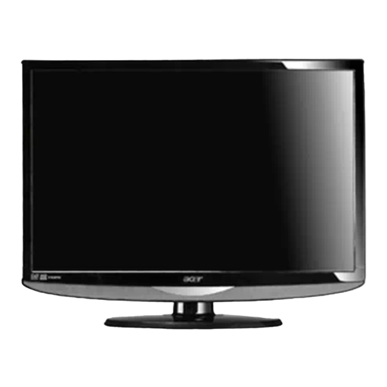
- Page 1 Acer AT3245 & AT3246 Service Guide...
- Page 2 Service Guide Version and Revision Version Date Revision History TPV Model Name Apr.-25-08 Initial release E328M2NBWAAZN...
- Page 3 Any Acer Incorporated software described in this manual is sold or licensed "as is". Should the programs prove defective following their purchase, the buyer (and not Acer Incorporated, its distributor, or its dealer) assumes the entire cost of all necessary servicing, repair, and any incidental or consequential damages resulting from any defect in the software.
- Page 4 DIFFERENT part number code to those given in the FRU list of this printed Service Guide. You MUST use the list provided by your regional Acer office to order FRU parts for repair and service of customer machines. Warning: (For FCC Certified Models) Note: This equipment has been tested and found to comply with the limits for a Class B digital device, pursuant to Part 15 of the FCC Rules.
- Page 5 Precautions Do not use the monitor near water, e.g. near a bathtub, washbowl, kitchen sink, laundry tub, swimming pool or in a wet basement. Do not place the monitor on an unstable trolley, stand, or table. If the monitor falls, it can injure a person and cause serious damage to the appliance.
-
Page 6: Table Of Contents
Table Of Contents Monitor Features ……………………………………… General Specifications ……………………………………… LCD TV Description ……………………………………… Precautions And Notices ……………………………………… D-SUB PIN Distribution ……………………………………… Chapter 1 Factory Preset Display Modes ……………………………………… LCD TV Panel Specification ……………………………………… Panel Features ……………………………………… General Specifications ……………………………………… Mechanical Specifications ………………………………………... -
Page 7: Monitor Features
Chapter 1 Monitor Features General Specifications... -
Page 9: Lcd Tv Description
LCD TV Description The LCD TV will contain a main board (include audio), a switching power board, a function keyboard, an IR Board and a side board. The main board and power board will house the flat panel to control logic I2C bus, DDC, brightness control logic for LCD panel, DC-DC conversion to supply the appropriate power to the whole board and transmitting TTL level signals into LCD Module to drive the LCD display circuit. -
Page 10: D-Sub Pin Distribution
D-SUB PIN Distribution This procedure gives you instructions for installing and using the LCD TV display. (1) Position the display on the desired operation and plug the power cord into a convenient AC outlet. Three-wire power cord must be shielded and is provided as a safety precaution as it connects the chassis and cabinet to the electrical conduct ground. -
Page 11: Factory Preset Display Modes
Factory Preset Display Modes: VGA/HDMI Input Signal Reference Chart... -
Page 12: Lcd Tv Panel Specification
LCD TV Panel Specification V315B1- L01 is a 31.5” TFT Liquid Crystal Display module with 16-CCFL Backlight unit and 1ch-LVDS interface. This module supports 1366 x 768 WXGA format and can display true 16.7M colors ( 8-bit colors). The inverter module for backlight is built-in. -
Page 13: Optical Specifications
Electrical Characteristics Optical Specifications Test Conditions Optical Specifications... -
Page 14: Connecting Peripherals
Chapter 2 Connecting Peripherals Front panel controls... -
Page 15: Remote Control & Osd Operating Instructions
Chapter 3 Remote Control & OSD Operating instructions Using the Remote Control 5 e (Empowering Technology) Press to activate Acer Empowering Technology. See page 25. 6 MENU Press to open or close the Menu. 7 Back Press to back to previous Menu. - Page 16 Teletext 1 Color buttons (R/G/Y/B) Operates corresponding button on the teletext page. 2 INDEX Press to go to the index page. 3 SUBTITLE Press to view subtitles on the screen. 4 REVEAL Press to reveal hidden teletext information. 5 SUBPAGE Press to access the teletext’s subpages directly.
-
Page 17: Using The Osd Menus
Using the OSD Menus... -
Page 25: Logo
Logo When the monitor is power on, the LOGO will be showed in the center, and disappear slowly. How To Optimize The DOS-Mode Plug And Play Plug & Play DDC2B Feature This monitor is equipped with VESA DDC2B capabilities according to the VESA DDC STANDARD. It allows the monitor to inform the host system of its identity and, depending on the level of DDC used, communicate additional information about its display capabilities. -
Page 26: Chapter 4 Machine Disassembly
Chapter 4 Machine Disassembly This chapter contains step-by-step procedures on how to disassemble the monitor for maintenance. The tools listed as below are that we may use during this procedure: 1. A proper screwdriver 2. A pair of glove 3. A pliers 4. - Page 27 3. Remove 4 screws to remove the bkt-vesa-top. 4. Release the connectors.
- Page 28 5. Remove the speakers. 6. Remove the main board, power board...
- Page 29 7. Remove the bkt-PCB-holder. 8. Release the key board and IR board. 9. Remove the BKT-panel-support.
- Page 30 10. Remove the bezel. 11. Remove the 6 screws to release the panel.
-
Page 31: Chapter 5 Trouble Shooting
Chapter 5 Trouble Shooting No picture (LED orange) No picture Check key board/IR board Change key board/IR board Check 24V power supply Check the power supply circuit Check main board Standby power supply Change U152 Check U400 Change U400 Check I C communication Check I C bus... - Page 32 Abnormal display Reset source Check the source Replace the filter or resistance Check signal filter circuit RF signal Check TV system setup Check input Check LVDS cable Replace LVDS cable Check Tuner Check panel Replace panel Replace Tuner No sound Reset source Check the source Check if mute...
- Page 33 No Power (No LED indicator) Plug in power cord and interface Check power cord and board interface Replace F901 or BD901 or C907 Check F901, BD901, C907 Check IC931, Q931 Replace IC931 or Q931 Replace T931 Check T931 Check D935, C926, C928 Replace D935 or C926 or C928 No display (LED indicator green) Check the source...
- Page 34 Key Board OSD is unstable or not working Is Key Pad Board connecting normally? Connect Key Pad Board Replace Button Switch Is Button Switch normally? Is Key Pad Board Normally? Replace Key Pad Board Check Main Board...
-
Page 35: Chapter 6 Upgrade Firmware
Chapter 6 Upgrade Firmware Step 1: Install USB driver to your computer from the ISP board USB Driver file. ISP board USB driver include three files: 1. PL-2303 Driver InstallerV2021.exe 2. ser2pl.sys 3. UTS2pl.sys 4. Install PL-2303 Driver InstallerV2021.exe Push "Next". - Page 36 Push "Finish". 5. ser2pl.sys & UTS2pl.sys two files should copy to C:\WINDOWS\system32\drivers & replace original files.
- Page 37 Step 2: Connect to ISP Board. Use USB port connecting PC & MT537x (or MT****) Board via ISP board(Code number: 715G537XL2). USB Cable Use Desktop PC or Notebook USB Port Step 3: Update TV. I. Open the MtkTool to Load .bin file (Example: F3_dbg_image.bin) & Set Auto Set Flash BaudRate...
- Page 39 II. Set COM port resource that used by USB Port. III. Set Baud rate 115200 & High speed item Enable. & MT537x(MT****).
- Page 40 IV. Click "Upgrade" button.(Waiting for "Finished!" message.) V. Main board Power Off _ On.
-
Page 41: Chapter 7 White-Balance, Luminance Adjustment
Chapter 7 White-Balance, Luminance Adjustment Approximately 30 minutes should be allowed for warm up before proceeding white balance adjustment. YPbPr Mode display adjustment White balance adjustment (B) General set-up : Equipment Requirements: Minolta CA-110 or Equivalent Color analyzer Quantum Data Pattern Generator 802G , 802BT or equivalent instrument Input requirements: Input Signal Type : YPbPr signal 1. - Page 42 Color temperature Standard/Warm/Cold (x, y) co-ordinates specification: Picture Mode Normal (10000 0.281±0.005 0.288±0.005 Warm (8000 0.295±0.005 0.305±0.005 Cold (13000 0.269±0.005 0.274±0.005 Table: Reading with Minolta CA-110. Note: 1. Use Minolta CA-110 for color coordinates and luminance check. 2. Luminance > 400 cd/m in the center of the screen when Brightness control at 100;...
-
Page 43: Fru (Field Replaceable Unit) List
Service Guide. For ACER AUTHORIZED SERVICE PROVIDERS, your Acer office may have a DIFFERENT part number code from those given in the FRU list of this printed Service Guide. You MUST use the local FRU list provided by your regional Acer office to order FRU parts for repair and service of customer machines. -
Page 44: Exploded Diagram
Exploded Diagram (Model: AT3245 & AT3246) -
Page 45: Edid Data
EDID Data DDC DATA for For D-SUB Input EDID data (128 bytes) **********************************************************************... -
Page 46: Chapter 9 Pcb Layout
Chapter 9 PCB Layout Main Board Layout... - Page 48 Power Board...
- Page 49 Key Board IR board...
-
Page 50: Chapter 10 Schematic Diagram
Chapter 10 Schematic Diagram Main Board EU OTS MT533X - 4 LAYERS STB_PWR5V +5V_STB FB100 220R/2000mA +24V 2,6,16 +24V +5V_STB +5V_SW +12V 2,16 +12V FB101 220R/2000mA +5V_STB 2,9,11 +5V_STB +5V_SW 2,7,10,12,13,14,15,16,17 +5V_SW C107 C106 +5V1_TUN +5V1_TUN 100N 16V Q104 SI5441DC DV18_DDR DV18_DDR DV11... - Page 51 +24V Add Thermal Pad 1,6,16 +24V +12V 1,16 +12V +5V_STB 1,9,11 +5V_STB +5V_STB +3V3SB +5V_SW AV33 +24V +12V +3V3SB Panel VCC=5V 1,11 +3V3SB U152 U151 AME8810-AEGTZ 0.6A/3.3V +5V_SW 1,7,10,12,13,14,15,16,17 +5V_SW LD1117DT33TR R177 R176 +5V_TUNER VIN VOUT VOUT(heat sink) +5V_TUNER 0R05 1/4W +5V1_TUN NC/0R05 1/4W +5V1_TUN...
- Page 52 +5V_TUNER +5V_TUNER +5V_T +5V_T +5V_T +5V_T +5V_TUNER AV25 2,14 AV25 FB202 FB203 FB204 FB201 1,2,4,5,6,7,8,9,10,11,12,13,14,15,16,17 +5V_T1 +5V_T2 +5V_T3 U400H MPX0P 120R/500mA 120R/500mA 120R/500mA 220R/2000mA MPX0P MPX0N AVDD25_SADC C206 C205 C215 C216 C217 C218 C201 C202 MPX0N AVDD25_SADC AVSS25_SADC 100N 16V 10U 10V 100N 16V 10U 10V...
- Page 53 DV18_12_DM FB230 DVDD18 Digital 1.8V Bypass Caps AV33 FB233 ADVDD33_1 AV33 FB232 AVDD33 1,2,3,5,6,7,8,9,10,11,12,13,14,15,16,17 Analog 3.3V Bypass Caps 600R/200mA C280 C232 C245 C236 C234 C246 600R/200mA 600R/200mA 10U 10V 100N 16V 100N 16V 100N 16V 100N 16V 100N 16V C283 C238 C239 C249...
- Page 54 1,2,3,4,6,7,8,9,10,11,12,13,14,15,16,17 DV11 DV33 DV33SB U400I 1,6,9,11,15,16,17 DV33SB DV33 1,2,4,6,9,10,15,16,17 DV33 DV18_DDR VCCK DV18_DDR DV11 VCCK DV11 AOBCK VCCK AOBCK C255 C259 C271 C273 C265 C252 AOLRCK VCCK AOLRCK 4.7UF 10V 100N 16V 100N 16V 100N 16V 100N 16V 1UF 6V3 VCCK OPWM0 VCCK...
- Page 55 Strapping R318 R325 U400B Support CI 4.7K 1,2,3,4,5,7,8,9,10,11,12,13,14,15,16,17 MAIN_SDA TP301 No Support CI 4.7K +3V3SB OSDA0 GPIO_0 1,2,11 +3V3SB MAIN_SCL TP300 +12V OSCL0 GPIO_1 1,2,16 +12V HDMI1_SDA HPDET R318 0402/SMD DV33 OSDA1 GPIO_2 1,2,4,5,9,10,15,16,17 DV33 HDMI1_SCL RESET_CI NC/4K7 1/16W 5% DV33SB DV33 OSCL1...
- Page 56 1,2,3,4,5,6,8,9,10,11,12,13,14,15,16,17 AV12 FB321 +5V_SW 1,2,10,12,13,14,15,16,17 +5V_SW AVDD12_PLL AV33 U400D 2,4,15,16,17 AV33 120R/500mA AV12 2,13,15 AV12 USB_VRT AVDD12_PLL USB_VRT AVDD12_ADCPLL USB_DM AVDD12_PLL C321 C322 C323 C324 C325 USB_DM AVDD12_PSCANPLL USB_DP AVDD12_PLL 100uF 16V 1uF/16V 4UF7 10V 100N 16V 10N 16V USB_DP AVDD12_DTDPLL AVDD12_PLL HV TYPE...
- Page 57 U400A U351 U352 1,2,3,4,5,6,7,9,10,11,12,13,14,15,16,17 RDQS0 RA12 RDQS0 RA12 RDQS0# RA11 RDQ0 RDQ16 DV18_DDR RDQS0_ RA11 DV18_DDR RDQM0 RA10 RDQ1 RDQ17 MEM_VREF RDQM0 RA10 MEM_VREF RDQ0 RDQ2 RDQ18 RDQ0 RDQ1 RDQ3 RDQ19 RDQ1 RDQ2 RDQ4 RDQ20 RDQ2 RDQ3 RDQ5 RDQ21 RDQ3 RDQ4 RDQ6 RDQ22...
- Page 58 U400J 1,2,3,4,5,6,7,8,10,11,12,13,14,15,16,17 POCE0# AB15 U0RX +5V_STB POCE0_ U0RX 1,2,11 +5V_STB CI_POCE1# AC15 U0TX DV33 U390 DV33 DV33SB POCE1_ U0TX 1,5,6,11,15,16,17 DV33SB POOE# U2RX TP391 MX25L3205DMI-12G DV33 POOE_ U2RX 1,2,4,5,6,10,15,16,17 DV33 CI_POWE# U2TX TP392 DV33 POOE# POWE_ U2TX HOLD SCLK PDD0 DV33 PDD1 NVM_WEN...
- Page 59 1,2,3,4,5,6,7,8,9,11,12,13,14,15,16,17 CLOSE TO CI CONNECTOR +5V_SW 1,2,7,12,13,14,15,16,17 +5V_SW DV33 CLOSE TO CI CONNECTOR 1,2,4,5,6,9,15,16,17 DV33 CI_VCC CI_VCC +5V_SW +5V_SW CI_DV33 CI_DV33 DV18_CI DV18_CI FB405 NC/220R/200mA +5V_SW R401 R402 R406 R408 R436 R435 FB404 CI_VCC CI_VPP 10K 1/10W 5% NC/10K 1/10W 5% 10K 1/10W 5% 10K 1/10W 5% 4K7 1/10W 5%...
- Page 60 +3V3SB KEY _UP_DN_DCSW KEY _UP_DN_DCSW +5V_STB 1,2,9 +5V_STB +3V3SB +3V3SB HDMI_CEC 6,15 HDMI_CEC CEC_PWR CEC_PWR MAIN_SCL MAIN_SCL CN450 MAIN_SDA MAIN_SDA 0402/SMD R450 NC/33R 1/16W 5% uP_SCL LED_G# LED_G# R451 NC/33R 1/16W 5% uP_SDA R480 NC/10K 1/10W 5% 0402/SMD RESET_CECMCU LED_R# LED_R# NC/63383 3P 2.0mm C457...
- Page 61 NEAR IO CONNECTOR NEAR MT533X D504 SCT2_AUR_OUT +5V_SW SCT2_AUR_OUT D506 NC/BAS316 SCT2_AUL_OUT SCT2_AUL_OUT NC/BAS316 +5V_SW SC2_LIN SC2_LIN L504 R529 R532 C520 47NF16V C512 10U 10V R523 SC2_RIN Full SCART SC2_RIN SCT1_AV_IN SC1_Y _CVBS_IN SCT1_AUR_IN SC1_RIN 0U10 H 20K 1/16W 5% SCT1_AUR_OUT SCT1_AUR_OUT 27 OHM +-5% 1/16W...
- Page 62 U400E AV1_RIN AV1_RIN HSY NC AC16 AV12 AV12 AV12 AV1_LIN HSY NC AV1_LIN VSY NC AB17 AD22 DVDD12_VGA L550 L551 L552 VSY NC DVDD12_VGA AF16 DVDD12_VGA AVDD12_RGBFE AVDD12_RGBADC VGA_RIN VGA_RIN AE16 AC21 AVDD12_RGBADC VGA_LIN AVDD12_RGBADC VGA_LIN AC17 AVDD12_RGBFE 0U10 H 0U10 H 0U10 H AVDD12_RGBFE...
- Page 63 NEAR AV CONNECTOR NEAR MT533X U400F AV25 AV25 CVBS0 AC26 AC25 GND_TUNER D650 CVBS0 GND_TUNER SIDE_CVBS_IN AD26 AD24 GND_CVBS +5V_SW CVBS1 GND_CVBS SIDE_Y _IN AD25 AF24 GND_SV SIDE_LIN CVBS2 GND_SV SIDE_LIN SIDE_C_IN AE26 Y 24 DVDD25_VADC NC/BAS316 CVBS3 DVDD25_VADC SC2_Y _CVBS_IN AF26 AA25 AVDD25_VADC...
- Page 64 +5V_SW 1,2,7,10,12,13,14,16,17 +5V_SW AV12 2,7,13 AV12 AV33 2,4,7,16,17 AV33 DV33SB 1,5,6,9,11,16,17 DV33SB DV33 1,2,4,5,6,9,10,16,17 DV33 EDID_WEN DV33SB 6,13 EDID_WEN HPD0 HPD0 HPD1 U400K HPD1 HPD2 HPD2 RX1_C- AE12 RX0_CB EXT_RES RX1_C+ AF12 R701 100R 1/16W 5% OPWR0_5V 0402/SMD D701 RX0_C OPWR0_5V L700 RX1_0-...
- Page 65 AV33 AV33 FB605 75R W6 RH 3.5X10X1.0 +5V_SW 1,2,7,10,12,13,14,15,17 +5V_SW WM_OP_VCC WM_OP_VCC VIMD_AADC REFP_AADC AVDD33_DIG +24V AUDIO-VDD +12V +12V FB601 FB602 +24V U400G 1,2,6 +24V 120R/500mA 120R/500mA 1,2,3,4,5,6,7,8,9,10,11,12,13,14,15,17 SC2_LIN TP601 C601 C602 C603 C604 C605 C606 C607 C608 C622 C623 AIN0_L ALIN 100uF 35V...
- Page 66 PANEL_VCC FB751 220R/2000mA FB752 220R/2000mA DV33 DV33 FB753 220R/2000mA NEAR CN750 C752 C751 CN750 100uF 16V 100N 16V HV TYPE PANEL_VCC PANEL_VCC +5V_SW 1,2,7,10,12,13,14,15,16 +5V_SW DV33 1,2,4,5,6,9,10,15,16 DV33 DV33SB 1,5,6,9,11,15,16 DV33SB 1,2,3,4,5,6,7,8,9,10,11,12,13,14,15,16 U400C OPWM1 OPWM1 INVERTER_SW INVERTER_SW AVDD33_LVDS BRIGHT_ADJ AVDD33_LVDS BRIGHT_ADJ AVDD33_LVDS INVERTER_ON_OFF...
- Page 67 Power board L906 L903 300uH D902 FB904 T931 73T 174122 L R938 R939 C924 C925 L932 POWER X'FMR DIODE FMN-1106S 10A/600V TO-220 47 OHM 1/4W 47 OHM 1/4W 0.001uF 0.001uF 3.5uH BEAD 93T 52 56 FB906 BEAD R923 71G 55 9 T C952 10K OHM 1/4W C923...
- Page 68 Key board NOTE Pull up R = 3.9K ohm to 3.3V SOURCE MENU VOL- VOL+ KEY1 1.04V 0.35V 2.44V 1.73V C001 0.1uF/25V SW001 SW002 SW003 SW004 R001 R002 R003 R004 4.3K OHM 1% 1/10W 1.8K OHM 1% 1/10W 470 OHM 1% 1/10W 11KOHM1/10W CN001 POWER...