Sony TA-E1 Service Manual
Hide thumbs
Also See for TA-E1:
- Service manual (18 pages) ,
- Operating instructions manual (32 pages) ,
- Operating instructions manual (28 pages)

Related Manuals for Sony TA-E1


Summary of Contents for Sony TA-E1
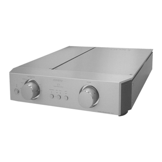
- Page 1 TA-E1 SERVICE MANUAL US Model Canadian Model AEP Model UK Model E Model Australian Model SPECIFICATIONS STEREO PRE AMPLIFIER MICROFILM Get user manuals: See SafeManuals.com...
-
Page 2: Table Of Contents
LES DIAGRAMMES SCHÉMATIQUES ET LA LISTE DES PIÈCES SONT CRITIQUES POUR LA SÉCURITÉ DE FONCTIONNEMENT. NE REMPLACER CES COMPOSANTS QUE PAR DES PIÈCES SONY DONT LES NUMÉROS SONT DONNÉS DANS CE MANUEL OU DANS LES SUPPLÉMENTS PUBLIÉS PAR SONY. Get user manuals:... -
Page 3: General
SECTION 1 This section is extracted from instruction manual. GENERAL Get user manuals: See SafeManuals.com... - Page 4 Get user manuals: See SafeManuals.com...
-
Page 5: Electrical Adjustment
TA-E1 SECTION 2 SECTION 3 ELECTRICAL ADJUSTMENTS DIAGRAMS IDLING ADJUSTMENT AND OFFSET VOLTAGE BALANCE OUTPUT LEVEL ADJUSTMENT 3-1. CIRCUIT BOARDS LOCATION CHECK • Perform this adjustment when replacing CP102. • Perform this adjustment after the idling adjustment • Perform this adjustment after replacing CP103 and CP104. -
Page 6: Schematic Diagram - Main Section (1/3)
TA-E1 3-2. SCHEMATIC DIAGRAM – MAIN SECTION (1/3) – • Refer to page 9 for Printed Wiring Board. (Page 8) (Page 7) (Page 7) (Page 7) (Page 7) (Page 10) Get user manuals: See SafeManuals.com... -
Page 7: Schematic Diagram - Main Section (2/3)
TA-E1 3-3. SCHEMATIC DIAGRAM – MAIN SECTION (2/3) – • Refer to page 9 for Printed Wiring Board. (Page 6) (Page 6) (Page 6) (Page 8) (Page 6) (Page 8) (Page 10) (Page 10) (Page 10) Get user manuals: See SafeManuals.com... -
Page 8: Schematic Diagram - Main Section (3/3)
TA-E1 3-4. SCHEMATIC DIAGRAM – MAIN SECTION (3/3) – (Page 6) (Page 7) (Page 7) Get user manuals: See SafeManuals.com... -
Page 9: Printed Wiring Board - Main Section
TA-E1 • Semiconductor Location 3-5. PRINTED WIRING BOARD – MAIN SECTION – Ref. No Location • Refer to page 5 for Circuit Boards Location. D201 D202 D203 D204 D205 D206 D207 D208 D209 D210 D211 B-10 D212 B-10 D401 D402... -
Page 10: Schematic Diagram - Power Section
TA-E1 3-6. SCHEMATIC DIAGRAM – POWER SECTION – (Page 6) (Page 7) (Page 7) (Page 7) Get user manuals: See SafeManuals.com... -
Page 11: Printed Wiring Board - Power Section
TA-E1 3-7. PRINTED WIRING BOARD – POWER SECTION – • Refer to page 5 for Circuit Boards Location. MAIN MAIN (Page 9) BOARD BOARD MAIN BOARD (Page 9) (Page 9) MAIN BOARD (Page 9) • Semiconductor Location Ref. No Location... -
Page 12: Exploded Views
SECTION 4 EXPLODED VIEWS 4-2. FRONT PANEL SECTION NOTE: The components identified by • Hardware (# mark) list and accessories and pack- • -XX, -X mean standardized parts, so they may have mark ! or dotted line with mark ing materials are given in the last of this parts list. some difference from the original one. -
Page 13: Bottom Plate Section
4-3. BOTTOM PLATE SECTION not supplied not supplied #8 (US, CND) #8 (US, CND) #7 (EXCEPT, #7 (EXCEPT, US, CND) US, CND) not supplied not supplied not supplied (US, CND) not supplied not supplied not supplied not supplied The components identified by mark ! Les composants identifiés par une or dotted line with mark ! are critical marque ! sont critiques pour la sécurité. -
Page 14: Electrical Parts List
AC J LED A SECTION 5 ELECTRICAL PARTS LIST LED B MAIN Note: • SEMICONDUCTORS • Due to standardization, replacements in the parts list The components identified by In each case, u: µ , for example: may be different from the parts specified in the mark ! or dotted line with mark uA...: µ... - Page 15 MAIN Ref. No. Part No. Description Remark Ref. No. Part No. Description Remark C403 1-128-200-11 ELECT 47uF CP103 1-418-107-11 AMPLIFIER UNIT C404 1-128-200-11 ELECT 47uF CP104 1-418-107-11 AMPLIFIER UNIT C405 1-110-512-51 FILM < DIODE > C406 1-110-512-51 FILM C407 1-128-972-11 ELECT 1000uF D201 8-719-800-76 DIODE 1SS226...
- Page 16 MAIN Ref. No. Part No. Description Remark Ref. No. Part No. Description Remark Q211 8-729-424-08 TRANSISTOR UN2111 R211 1-260-032-11 CARBON MELF 1/8W Q212 8-729-424-08 TRANSISTOR UN2111 R212 1-260-032-11 CARBON MELF 1/8W Q214 8-729-421-22 TRANSISTOR UN2211 R213 1-260-032-11 CARBON MELF 1/8W Q215 8-729-421-22 TRANSISTOR UN2211...
- Page 17 MAIN Ref. No. Part No. Description Remark Ref. No. Part No. Description Remark ! R516 1-202-937-41 FUSIBLE 1/2W < CAPACITOR > ! R517 1-202-937-41 FUSIBLE 1/2W ! R518 1-202-937-41 FUSIBLE 1/2W C701 1-136-880-11 FILM 2.2uF 160V C702 1-128-998-11 ELECT 6800uF R519 1-259-995-11 CARBON MELF 1/8W...
- Page 18 TA-E1 SW P SW L Ref. No. Part No. Description Remark Ref. No. Part No. Description Remark R709 1-259-995-11 CARBON MELF 1/8W < RESISTOR > ! R710 1-202-937-41 FUSIBLE 1/2W R601 1-260-008-11 CARBON MELF 1/8W ! R711 1-202-937-41 FUSIBLE 1/2W...