Table of Contents
Advertisement
Quick Links
Color Television
Contents
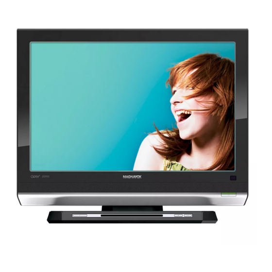
19MD358B
IR & LED Panel
Power Supply Panel: Adapter
Power Supply Panel: Inverter
©
Copyright 2008 Philips Consumer Electronics B.V. Eindhoven, The Netherlands.
All rights reserved. No part of this publication may be reproduced, stored in a
retrieval system or transmitted, in any form or by any means, electronic,
mechanical, photocopying, or otherwise without the prior permission of Philips.
Published by CS 0863 BU CD Consumer Care
Page
2
6
7
8
19
20
21
22
23
24
Diagram PWB
(SA01) 25
39-40
(SA02) 26
39-40
(SA03) 27
39-40
(SA04) 28
39-40
(SA05) 29
39-40
(SA06) 30
39-40
(SA07) 31
39-40
(SA08) 32
39-40
(SA09) 33
39-40
(SA10) 34
39-40
(SA11) 35
39-40
(SA12) 36
39-40
(SA13) 37
39-40
(SA14) 38
39-40
(KB01) 41
42
(IB01) 43
44
(PB01) 45
48-49
(PB02) 46
48-49
Printed in the Netherlands
Contents
Subject to modification
Chassis
TPM1.1U
LA
I_17550_000.eps
150208
Page
(PB03) 47
48-49
51
54
56
58
64
81
EN 3122 785 17551
Advertisement
Table of Contents

Related Manuals for Philips Magnavox 19MD358B


Summary of Contents for Philips Magnavox 19MD358B
-
Page 1: Table Of Contents
All rights reserved. No part of this publication may be reproduced, stored in a retrieval system or transmitted, in any form or by any means, electronic, mechanical, photocopying, or otherwise without the prior permission of Philips. Published by CS 0863 BU CD Consumer Care... -
Page 2: Technical Specifications, Connections, And Chassis Overview
EN 2 TPM1.1U LA Technical Specifications, Connections, and Chassis Overview 1. Technical Specifications, Connections, and Chassis Overview Index of this chapter: Product dimension (HxWxD) : 15.12” x 18.34” x 1.1 Technical Specifications 6.61”(19MF338B) 1.2 Connection Overview : 15.4” x 18.4” x 1.3 Chassis Overview 6.5”(19PFL3403D) : 15.62”... - Page 3 Technical Specifications, Connections, and Chassis Overview TPM1.1U LA EN 3 Chassis Overview 19MF338B I_17550_059.eps 060308 Figure 1-3 Chassis Overview...
- Page 4 EN 4 TPM1.1U LA Technical Specifications, Connections, and Chassis Overview 19PF3403D I_17550_060.eps 060308 Figure 1-4 Chassis Overview...
- Page 5 Technical Specifications, Connections, and Chassis Overview TPM1.1U LA EN 5 19MD358B I_17550_061.eps 060308 Figure 1-5 Chassis Overview...
-
Page 6: Safety Instructions, Warnings, And Notes
Be careful during measurements in the high voltage by the workshop during a repair: section. • Use only lead-free soldering tin Philips SAC305 with order • Never replace modules or other components while the unit code 0622 149 00106. If lead-free solder paste is required, is switched “on”. -
Page 7: Directions For Use
2006 week 17). The 6 last digits contain the It is easy to do, and is a good service precaution. serial number. 3. Directions for Use You can download this information from the following websites: http://www.philips.com/support http://www.p4c.philips.com... -
Page 8: Mechanical Instructions
EN 8 TPM1.1U LA Mechanical Instructions 4. Mechanical Instructions Index of this chapter: 1. Cable Dressing Notes: 2. Service Positions • Figures below can deviate slightly from the actual situation, 3. Assy/Panel Removal due to the different set executions. 4. Re-assembly •... - Page 9 Mechanical Instructions TPM1.1U LA EN 9 I_17550_063.eps 060308 Figure 4-2 Cable dressing(19PFL3403D)
- Page 10 EN 10 TPM1.1U LA Mechanical Instructions I_17550_064.eps 060308 Figure 4-3 Cable dressing (19MD358B)
- Page 11 Mechanical Instructions TPM1.1U LA EN 11 Service Positions Assy/Panel Removal For easy servicing of this set, there are a few possibilities 4.3.1 Stand/Base created: • The buffers from the packaging (see figure "Rear cover"). Remove the screws remarked in red to remove the stand or •...
- Page 12 EN 12 TPM1.1U LA Mechanical Instructions 4.3.2 Rear Cover 4.3.3 Power Board 1. Remove the screws remarked in red, which secure the rear 1. Refer to next figure cover. The screws are located at the top, bottom, left and 2. Unplug connector remarked in blue. right sides.
- Page 13 Mechanical Instructions TPM1.1U LA EN 13 4.3.4 Main Board 19MD358B 1. Refer to next figure 2. Unplug connector remarked in blue. 3. Replease screws remarked in red and remove the board. When defective, replace the whole unit. 19MF338B I_17550_073.eps 060308 Figure 4-14 Main Board 4.3.5 IR Board...
- Page 14 EN 14 TPM1.1U LA Mechanical Instructions 19PFL3403D 4.3.8 Bracket 1. Refer to next two figures. 2. Remove the screws remarked in red. I_17550_070.eps 060308 Figure 4-16 IR Board 4.3.6 Speakers I_17550_009.eps 120208 1. Refer to next figure. Figure 4-19 Bracket 2.
- Page 15 Mechanical Instructions TPM1.1U LA EN 15 19MD358B DVD Base Removal 4.4.1 Cover_BOTTOM_DVD_Base Remove the screws remarked in red to remove the Cover_BOTTOM_DVD_Base. I_17550_077.eps 060308 Figure 4-23 Rear Cover(19MD358B) Set Re-assembly I_17550_074.eps 060308 To re-assemble the whole set, execute all processes in reverse Figure 4-20 Cover_BOTTOM_DVD_Base order.
-
Page 16: Service Modes, Error Codes, And Fault Finding
EN 16 TPM1.1U LA Service Modes, Error Codes, and Fault Finding 5. Service Modes, Error Codes, and Fault Finding Index of this chapter: Also new in this chassis:when you activate CSM and there is a 5.1 Test Points USB stick connected to the TV,the software will dump the 5.2 Service Mode complete CSM content to the USB stick,The file(CSM.txt) will 5.3 Service Tools... - Page 17 5.3.1 ComPair Introduction ComPair (Computer Aided Repair) is a Service tool for Philips Consumer Electronics products. and offers the following: 1. ComPair helps you to quickly get an understanding on how to repair the chassis in a short and effective way.
- Page 18 EN 18 TPM1.1U LA Service Modes, Error Codes, and Fault Finding Personal Notes: E_06532_012.eps 131004...
-
Page 19: Block Diagrams, Test Point Overview, And Waveforms
Block Diagrams, Test Point Overview, and Waveforms TPM1.1U LA 6. Block Diagrams, Test Point Overview, and Waveforms Wiring Diagram 19MF338B WIRING DIAGRAM CN016 Key Board 3Pin Panel 89T179E30C919 FFC Cable 95T801412F901 2pin 2pin 11 Pin 11 pin 30 pin HARNESS 75120 CN601 CN602 CN902... -
Page 20: Wiring Diagram 19Pfl3403D
Block Diagrams, Test Point Overview, and Waveforms TPM1.1U LA Wiring Diagram 19PFL3403D WIRING DIAGRAM 95T8014 4F902 Panel Board HARNESS 75129 4 Pin 89T179E30C920 CN016 FFC Cable 95T801412X901 2 Pin 2 Pin 12 Pin 11 pin 30 Pin HARNESS 75120 CN902 CN101 CN701 CN601... -
Page 21: Wiring Diagram 19Md358B
Block Diagrams, Test Point Overview, and Waveforms TPM1.1U LA Wiring Diagram 19MD358B WIRING DIAGRAM CN016 Key Board 3Pin Panel 89T179E30C919 095T801412X90 4pin 6pin FFC CABLE 30P 2pin 2pin 11 Pin 11 pin HARNESS TE0002 CN303 CN601 CN150 CN602 30 pin CN902 CN101 95T8014 4X901... -
Page 22: Block Diagram Power Supply
Block Diagrams, Test Point Overview, and Waveforms TPM1.1U LA Block Diagram Power Supply POWER SUPPLY IR 2mA +5V / LC +3V3SB LD1117S33 filter to +5Vc/60mA 5mA for WT6702 (Optional) +5Vc DV33SB SW_SI3441 / 50mA 50mA for MTK5380 +12V RC filter x 1 + LC filter x 3 Tuner +5V_TUNER 0.35A Alps 507A AV33 LD1117S33 350mA for MT5380... -
Page 23: Block Diagram Scaler Board 19Mf338B
Block Diagrams, Test Point Overview, and Waveforms TPM1.1U LA Block Diagram Scaler Board 19MF338B & 19MD358B ( Magnavox ) Function block of main Board w/ MT5380 ( Magnavox ) Function block of main Board w/ MT5380 Serial Flash 4MByte DDR1 256Mbit x1 SB-06 SB-04 Combo... -
Page 24: Block Diagram Scaler Board 19Pfl3403D
Block Diagrams, Test Point Overview, and Waveforms TPM1.1U LA Block Diagram Scaler Board 19PFL3403D Function block of main Board w/ MT5380 Function block of main Board w/ MT5380 WT61P7-RN440WT DDR1 256Mbit x1 ECE MCU SB-14 SB-04 Combo Tuner MT5380ACU Serial Flash 32 MByte IFAT +/- TDQU4-507A SB-06... -
Page 25: Circuit Diagrams And Pwb Layouts
Circuit Diagrams and PWB Layouts TPM1.1U LA 7. Circuit Diagrams and PWB Layouts Scaler Board: Power Part 1 SCALAR BOARD: POWER 1 SB01 SB01 CN101 A1 C101 C2 63391 11P 2.0MM C102 C2 C103 A3 C104 A4 C105 A4 R101 C106 A4 C107 A5 4K7 1/10W 5%... -
Page 26: (Sa02)
Circuit Diagrams and PWB Layouts TPM1.1U LA Scaler Board: Power Part 2 CN150 D4 SCALAR BOARD: POWER 2 C150 A1 SB02 SB02 C151 A1 C152 A2 C153 A2 C154 C1 AV25 OPWRSB C155 A4 U151 {2,6} OPWRSB +5V_SW U150 LD1117S33 AV33 AV12 C156 B6... -
Page 27: Scaler Board: Tuner/Usb/Itv
Circuit Diagrams and PWB Layouts TPM1.1U LA Scaler Board: Tuner / USB / ITV CN231 C8 CN232 D8 SCALER BOARD: TUNER/USB/ITV SB03 SB03 C200 D2 C201 C1 C202 A1 C203 A5 C204 A5 C205 A6 C206 A6 C207 A6 C208 A3 C209 A4 AV12 AV12... -
Page 28: Scaler Board: Ddr1 Memory
Circuit Diagrams and PWB Layouts TPM1.1U LA Scaler Board: DDR1 Memory C250 D4 C251 D5 C252 D5 C253 D1 SCALER BOARD: DDR1 MEMORY SB04 SB04 C254 D1 C255 D2 C256 D2 C257 D2 C258 D2 C259 D3 C260 D3 C261 D1 U400A C262 E4 C263 E4... -
Page 29: Scaler Board: Mt5380Peripheral
Circuit Diagrams and PWB Layouts TPM1.1U LA Scaler Board: MT5380 Peripheral CN301 D4 C N302 D6 SCALER BOARD: MT5380PERIPHERAL CN303 C7 C 301 C1 SB05 SB05 C302 A4 C 303 B3 C304 A5 C 305 A6 C306 C7 C 307 C8 C308 B6 C 309 D7 U400B... -
Page 30: Scaler Board: Flash/Jtag/Uart
Circuit Diagrams and PWB Layouts TPM1.1U LA Scaler Board: Flash / JTAG / UART CN351 B6 C 350 A3 SCALER BOARD: FLASH/JTAG/UART C352 C5 C 353 C5 SB06 SB06 C354 C5 C 355 C6 C356 C6 C 357 D5 C358 D5 C 359 D5 C360 D6 C 361 D6... -
Page 31: Scaler Board: Hdmi
Circuit Diagrams and PWB Layouts TPM1.1U LA Scaler Board: HDMI CN401 A5 C 401 A4 SCALER BOARD: HDMI C402 B1 C 403 B8 SB07 SB07 C404 B8 C 405 B7 C406 C7 C 407 C8 C408 C8 D 401 A3 D402 B1 D 403 B4 D404 C4 D... -
Page 32: Scaler Board: Vga In/Lr
Circuit Diagrams and PWB Layouts TPM1.1U LA Scaler Board: VGA In / LR CN450 A1 SCALER BOARD: VGA IN/LR CN451 D1 SB08 SB08 C424 D6 C450 A2 C451 A6 C452 A6 C453 A5 C454 A6 NEARLY VGA CON. NEARLY IC C455 B6 {10} +5V_SW... -
Page 33: Scaler Board: Ypbpr/L/R In
Circuit Diagrams and PWB Layouts TPM1.1U LA Scaler Board: YPbPr/L/R In SCALER BOARD: YPBPR/L/R IN SB09 SB09 CN501 C1 AV12 FB501 AV12 FB502 CN502 D1 HSYNC C501 A4 U400E HSYNC AVDD12_RGBADC DVDD12_VGA VSYNC VSYNC C502 A4 SOY0 DVDD12_VGA 120R/500mA 120R/500mA SOY0 DVDD12_VGA C503 A5... -
Page 34: Scaler Board: Cvbs/L/R In
Circuit Diagrams and PWB Layouts TPM1.1U LA Scaler Board: CVBS/L/R In CN550 B1 CN 551 D1 SCALER BOARD: CVBS/L/R IN C550 B1 C552 D6 SB10 SB10 C553 D5 C554 D6 C555 D6 C556 E5 C559 A3 C560 A4 C561 A4 C562 B6 AV25 FB550 AV25... -
Page 35: Scaler Board: Audio Amplifier
Circuit Diagrams and PWB Layouts TPM1.1U LA Scaler Board: Audio Amplifier CN601 B6 CN602 A6 SCALER BOARD: AUDIO AMP C601 D4 C602 D7 SB11 SB11 C603 B3 C604 E3 C606 B4 C607 B5 C608 B4 C609 C7 C610 C6 C611 C4 C612 C6 C613 C7 *** PRINT "+/-"... -
Page 36: Scaler Board: Headphone
Circuit Diagrams and PWB Layouts TPM1.1U LA Scaler Board: Headphone CN650 D8 SCALER BOARD: HEADPHONE C650 A4 SB12 SB12 C651 A4 C652 A5 C653 A6 C654 A6 C655 A6 AV33 FB650 U400G C656 A6 AV33 FB651 AVDD33_AADC C657 B4 AIN0_L ASPDIF 120R/500mA C658 B5... -
Page 37: Scaler Board: Lvds Out
Circuit Diagrams and PWB Layouts TPM1.1U LA Scaler Board: LVDS Out SCALER BOARD: LVDS OUT SB13 SB13 U400C AV33 FB701 AVDD33_LVDS AVDD33_LVDSA AVDD33_LVDS AVDD33_VPLL AVDD33_LVDSB AVDD33_LVDS AVDD33_LVDSC 120R/500mA AVDD33_VPLL AVDD33_VPLL C701 C702 C703 INVERTER_ON_OFF INVERTER_ON_OFF CK1N 100uF 16V 1uF/16V 100N 16V CK1N CK1P TP701... -
Page 38: Scaler Board: Dvd Interface
Circuit Diagrams and PWB Layouts TPM1.1U LA Scaler Board: DVD Interface CN750 B1 C750 C3 SCALER BOARD: DVD INTERFACE C751 A7 SB14 SB14 C752 A7 C753 B7 C754 B7 C755 B6 C756 C7 C757 C6 C758 C7 NEARLY YPBPR CONNECTOR NEARLY MT5380 C759 D5 C760 E5... - Page 39 Circuit Diagrams and PWB Layouts TPM1.1U LA Layout Scaler Board (Top Side) C101 A2 C264 B2 C628 A5 D505 D3 R190 A3 R465 E2 R714 A1 C102 A2 C265 B2 C629 A5 D550 D5 R191 A3 R466 C3 R715 A1 C103 C1 C266 B2 C630 A5...
- Page 40 Circuit Diagrams and PWB Layouts TPM1.1U LA Layout Scaler Board (Bottom Side) C172 A4 FB550 C3 C205 B4 FB551 C3 C206 B4 FB552 C3 C208 C3 FB553 C3 C209 B3 FB650 B3 C210 B3 FB651 B3 C211 B3 FB652 B3 C217 C2 FB653 B3 C218 C2...
-
Page 41: Keyboard & Control Panel
Circuit Diagrams and PWB Layouts TPM1.1U LA Keyboard & Control Panel CN016 B1 KEYBOARD & CONTROL PANEL C016 C1 KB01 KB01 C017 C2 C018 A2 C019 A2 C020 A3 C021 A3 Menu VOL- VOL+ C022 A4 C023 A4 KEY_MENU_L_R C024 C4 C019 C021 C023... - Page 42 Circuit Diagrams and PWB Layouts TPM1.1U LA Layout Keyboard & Control Panel (Top Side) Personal Notes: CN016 A2 SW016 A3 SW017 A2 SW018 A3 SW019 A4 SW020 A5 I_17550_041.eps 150208 Layout Keyboard & Control Panel (Bottom Side) C016 A2 C020 A2 C024 A5 R016 A4 R020 A3...
-
Page 43: Ib01
Circuit Diagrams and PWB Layouts TPM1.1U LA IR & LED Panel CN001 B1 IR & LED PANEL C001 D4 IB01 IB01 C002 D4 C003 C2 C004 C3 C005 C2 LED001 B5 Q001 B5 R001 A5 R002 B5 POWER R003 C4 +5V_STB R004 C4 SW001... - Page 44 Circuit Diagrams and PWB Layouts TPM1.1U LA Layout IR & LED Panel (Top Side) Personal Notes: C001 C002 C003 C004 C005 CN001 LED001 B2 Q001 R001 R002 R003 R004 SW001 U001 ZD001 ZD002 I_17550_044.eps 150208 E_06532_012.eps 131004...
-
Page 45: Pb01
Circuit Diagrams and PWB Layouts TPM1.1U LA Power Supply Panel: Adapter BD901 A1 CN901 E1 CN902 A8 C900 B1 PSU: ADAPTER PB01 PB01 C901 B1 C905 C5 C906 C5 C907 A2 C908 D1 C909 D7 R916 100 OHM 1/4W C918 C930 C931 C911 B6 C912 C4... -
Page 46: Pb02
Circuit Diagrams and PWB Layouts TPM1.1U LA Power Supply Panel: Inverter CN821 A10 CN823 B10 CN824 C10 CN825 D10 PSU: INVERTER CN831 A10 CN833 C10 PB02 PB02 CN851 C10 CN853 E10 C801 A7 C802 A7 C805 B7 C806 C7 C807 C8 C810 E7 C811 B3 C812 D4 C813 C4 C819 E3 C820 B5 C821 B5... -
Page 47: Power Supply Panel: Jumper
Circuit Diagrams and PWB Layouts TPM1.1U LA Power Supply Panel: Jumper F901 B1 PSU: JUMPER PB03 PB03 J801 B1 J802 B1 J803 B1 J804 B2 J805 B2 J806 B2 J807 B3 J901 A1 J903 A2 J904 A2 J901 J903 J904 J905 J906 J907... - Page 48 Circuit Diagrams and PWB Layouts TPM1.1U LA Layout Power Supply Panel (Top Side) BD901 B2 C806 C840 C906 C913 C920 CN823 A2 CN833 A2 CN902 C5 D905 HD902 B5 IC903 D4 J804 J902 J906 L902 PT801 A2 R834 R861 R934 T901 C801 C807...
- Page 49 Circuit Diagrams and PWB Layouts TPM1.1U LA Layout Power Supply Panel (Bottom Side) C803 B2 C822 A2 C838 B2 C860 B2 C883 A3 C923 C3 D831 A2 D887 A4 Q841 A4 Q885 A4 R811 A3 R821 A2 R835 B2 R849 B4 R863 A3 R882 A3 R900 C2...
- Page 50 Circuit Diagrams and PWB Layouts TPM1.1U LA Personal Notes: E_06532_013.eps 131004...
-
Page 51: Alignments
Alignments TPM1.1U LA EN 51 8. Alignments Index of this chapter: Inital Set-up:Set Smart picure 8.1 Electrical Instructions as"Personal",Brightness=50,Color=50,Contrast=50.Then run 8.2 Serial Number Definition factory "AUTO-COLOR" proces. Alignment method: Initial Set-up:Set Smart picture Note: . The Service Mode are describe in chapter 5.Menu as"Personal"(Brightness=50,Color=50,Contrast=50) and navigation is done with the CURSOR UP, DOWN, LEFT or check Factory "SP_MODE_PWM"... - Page 52 EN 52 TPM1.1U LA Alignments Input Injection Point : AV1 YPbPr (RAC jack) 1080i, TVBar100 Check the gray pattern should be distinguished and color bar is pattern. correct. Alignment method: Check Luminance Note: 1.Initial Set-up:Select source as AV1 Use Minolta CA-210 for colour coordinates and luminance 2.
- Page 53 Alignments TPM1.1U LA EN 53 Table 8-8 Reading in Minolta CA-210. Normal/ (7500 Warm/(6500 Cool/(9300 K) x (center) 0.300 ± 0.010 0.314 ± 0.010 0.285 ± 0.010 y (center) 0.310 ± 0.010 0.324 ± 0.010 0.293 ± 0.010 Y (center) 19PFL3403D Equipment Requirements: Minolta CA-110 or CA-210 or Equivalent Color analyzer Chroma 2250 or equivalent PC...
-
Page 54: Circuit Descriptions, Abbreviation List, And Ic Data Sheets
EN 54 TPM1.1U LA Circuit Descriptions, Abbreviation List, and IC Data Sheets 9. Circuit Descriptions, Abbreviation List, and IC Data Sheets Index of this chapter: MediaTek MT5380ACU as scaler engine,which has embedded 9.1 Introduction Analog D-SUB,digital HDMI receiver,scaling input signal to 9.2 Block Diagram panel OSD mapping and simple 3D de-interlacer.The extra 9.3 Abbreviation List... - Page 55 Circuit Descriptions, Abbreviation List, and IC Data Sheets TPM1.1U LA EN 55 19PFL3403D Function block of main Board w/ MT5380 Function block of main Board w/ MT5380 Serial Flash 32 MByte DDR1 256Mbit x1 SB-06 SB-04 Combo Tuner MT5380ACU IFAT +/- TDQU4-507A .MCU CVBS + 2nd I F...
-
Page 56: Abbreviation List
Acer Unipack Optronics the customers wishes Asia Pacific LATAM LATin AMerica Aspect Ratio: 4 by 3 or 16 by 9 LC04 Philips chassis name for LCD TV 2004 Automatic Standard Detection project Audio Video Liquid Crystal Display B-TXT Blue teletext... - Page 57 SouND SNDS-VL-OUT Surround sound left variable level out SNDS-VR-OUT Surround sound right variable level out SOPS Self Oscillating Power Supply S/PDIF Sony Philips Digital InterFace SRAM Static RAM STBY Stand-by SVHS Super Video Home System Sub Woofer / SoftWare Total Harmonic Distortion...
-
Page 58: Ic Data Sheets
EN 58 TPM1.1U LA Circuit Descriptions, Abbreviation List, and IC Data Sheets IC Data Sheets This section shows the internal block diagrams and pin layouts of ICs that are drawn as "black boxes" in the electrical diagrams (with the exception of "memory" and "logic" ICs). 9.4.1 Diagram B1A, MT5380ACU I_17550_056.eps... - Page 59 Circuit Descriptions, Abbreviation List, and IC Data Sheets TPM1.1U LA EN 59 OSCREF OSCIO DDP1 OSCILLATOR BOOT1 IN1P DRIVER HIGH MODULATOR OUT1 CTRL IN1N DRIVER SSP1 STABI 11V STAB1 INREF SSP1 MANAGER STABI 11V STAB2 SSP2 BOOT2 IN2P DDP2 DRIVER HIGH MODULATOR OUT2...
- Page 60 EN 60 TPM1.1U LA Circuit Descriptions, Abbreviation List, and IC Data Sheets 9.4.3 Diagram B3A, NT5DS16M16CS-5T DQ15 DQ14 DQ13 DQ12 DQ11 DQ10 LDQS UDQS LDM* UDM* A10/AP A10/AP A10/AP 66-pin Plastic TSOP-II 400mil 16Mb x 16 32Mb x 8 64Mb x 4 Column Address Table Organization Column Address...
- Page 61 Circuit Descriptions, Abbreviation List, and IC Data Sheets TPM1.1U LA EN 61 9.4.4 Diagram B4A,NT5DS16M16CS-5T Bank3 Bank2 Bank1 CK, CK Mode Registers 8192 Bank0 Memory Data Array (8192 x 1024 x 8) Sense Amplifiers Generator DQ0-DQ3, COL0 Input I/O Gating Register DM Mask Logic Mask...
- Page 62 EN 62 TPM1.1U LA Circuit Descriptions, Abbreviation List, and IC Data Sheets 9.4.5 Diagram B5A, NT5DS16M16CS-5T Bank3 Bank2 Bank1 CK, CK Mode Registers 8192 Bank0 Memory Data Array (8192 x 512 x 16) Sense Amplifiers Generator DQ0-DQ7, COL0 Input I/O Gating Register DM Mask Logic A0-A12,...
- Page 63 Circuit Descriptions, Abbreviation List, and IC Data Sheets TPM1.1U LA EN 63 9.4.6 Diagram B6A, NT5DS16M16CS-5T Bank3 Bank2 Bank1 CK, CK Mode Registers 8192 Bank0 Memory Data Array (8192 x 256 x 32) Sense Amplifiers Generator DQ0-DQ15, LDM, UDM COL0 Input I/O Gating Register...
-
Page 64: Spare Parts List
EN 64 TPM1.1U LA Spare Parts List 10. Spare Parts List Position/Item PCM codes Philips 12NCs Description E07801 078T 497900 Z 996510011419 SPEAKER 4 OHM 3W 41x92mm E07801 078T 497901 M 996510011420 SPEAKER 4 OHM 3W 42x90mm E08901 089T402A18N IS... - Page 65 Spare Parts List TPM1.1U LA EN 65 C122 067T 305101 3C 996510011442 EC 100uF 16V KM 6.3x11mm C122 067T 305101 3E 996510011443 EC 100uF 16V RGA 6.3x11mm C123 067T 305220 4C 996510011444 EC 22uF 25V KM 5x11mm C125 065T060310412K Y 996510011563 CAP CHIP 0603 0.1UF K 16V X7R C150...
- Page 66 EN 66 TPM1.1U LA Spare Parts List C211 065T040210412K Y 996510011553 CAP CHIP 0402 100N 16V X7R C212 065T0603473 12 996510011575 CHIP 0603 47nF K 16V X7R C212 065T060347312K Y 996510011576 CAP CHIP 0603 47N 16V X7R C213 065T060310412K Y 996510011563 CAP CHIP 0603 0.1UF K 16V X7R C214...
- Page 67 Spare Parts List TPM1.1U LA EN 67 C266 065T0805475A2K 3 996510011583 CAP CHIP 4.7UF 10V X7R +/- 10% C267 067T 305220 4C 996510011444 EC 22uF 25V KM 5x11mm C268 065T040210412K Y 996510011553 CAP CHIP 0402 100N 16V X7R C269 065T040210412K Y 996510011553 CAP CHIP 0402 100N 16V X7R C270...
- Page 68 EN 68 TPM1.1U LA Spare Parts List C369 065T0603105 12 996510011565 CHIP 1UF 16V X7R C370 065T060310412K Y 996510011563 CAP CHIP 0603 0.1UF K 16V X7R C371 065T060310412K Y 996510011563 CAP CHIP 0603 0.1UF K 16V X7R C372 065T060310412K Y 996510011563 CAP CHIP 0603 0.1UF K 16V X7R C373...
- Page 69 Spare Parts List TPM1.1U LA EN 69 C560 065T0603105 12 996510011565 CHIP 1UF 16V X7R C561 065T040210412K Y 996510011553 CAP CHIP 0402 100N 16V X7R C562 065T0402472 22 996510011556 CHIP 4700pF 25V X7R C562 065T040247222K Y 996510011557 CAP CHIP 0402 4N7 25V X7R C563 065T060347031J Y 996510011573...
- Page 70 EN 70 TPM1.1U LA Spare Parts List C656 065T0402104 12 996510011551 CAP CHIP 0402 0.1UF 16V X7R C656 065T040210412K Y 996510011553 CAP CHIP 0402 100N 16V X7R C657 065T0603105 12 996510011565 CHIP 1UF 16V X7R C658 065T0402104 12 996510011551 CAP CHIP 0402 0.1UF 16V X7R C658 065T040210412K Y 996510011553...
- Page 71 Spare Parts List TPM1.1U LA EN 71 D401 093T 64S3PH 996510011599 BAS32L SOD80C D402 093T 64S3PH 996510011599 BAS32L SOD80C D403 093T 64S3PH 996510011599 BAS32L SOD80C D450 093T 64S3PH 996510011599 BAS32L SOD80C D451 093T 64S3PH 996510011599 BAS32L SOD80C D601 093T 64S3PH 996510011599 BAS32L SOD80C D602...
- Page 72 EN 72 TPM1.1U LA Spare Parts List Q101 057T 7601PH 996510002846 MUN2211TIG SC-59 Q102 057T 477900 T 996510011509 TRA BC847C 100mA/50V SOT-23 Q152 057T 7631PH 996510005852 SI5441DC 1206-8 Q153 057T 477900 T 996510011509 TRA BC847C 100mA/50V SOT-23 Q156 057T 7601PH 996510002846 MUN2211TIG SC-59 Q157...
- Page 73 Spare Parts List TPM1.1U LA EN 73 R250 061T0402000 Y 996510011514 RST CHIPR 0 OHM +-5% 1/16W R251 061T0603750 Y 996510011543 RST CHIPR 75 OHM +-5% 1/10W R252 061T0603750 Y 996510011543 RST CHIPR 75 OHM +-5% 1/10W R253 061T0603750 Y 996510011543 RST CHIPR 75 OHM +-5% 1/10W R254...
- Page 74 EN 74 TPM1.1U LA Spare Parts List R452 061T0402680 Y 996510011518 RST CHIP 68R 1/16W 5% R453 061T0603750 Y 996510011543 RST CHIPR 75 OHM +-5% 1/10W R454 061T0603000 Y 996510011519 RST CHIPR 0 OHM +-5% 1/10W R455 061T0402101 Y 996510011515 RST CHIP 100R 1/16W 5% R456 061T0402680 Y...
- Page 75 Spare Parts List TPM1.1U LA EN 75 R620 061T06032202FY 996510011526 RST CHIPR 22KOHM +-1% 1/10W R621 061T0603123 Y 996510011522 RST CHIPR 12KOHM +-5% 1/10W R622 061T06032202FY 996510011526 RST CHIPR 22KOHM +-1% 1/10W R623 061T0603105 Y 996510011493 RST CHIPR 1MOHM +-5% 1/10W R624 061T0603105 Y 996510011493...
- Page 76 EN 76 TPM1.1U LA Spare Parts List RP266 061T 126470 8Y 996510011513 RST CHIP AR 8P4R 75 OHM +-5% RP267 061T 126470 8Y 996510011513 RST CHIP AR 8P4R 75 OHM +-5% TU202 094TNTAT MA 1A 996510002821 TUNER TDQU4-507A U101 056T 563928 996500043934 IC LP2996MRX PSOP-8 U102...
- Page 77 FERRITE CORE 3.5 4.7 1 FB902 071T 55907 H 996510011702 FERRITE CORE 3.5 4.7 1 FB903 071T 55907 996510011701 FERRITE CORE 3.5 4.7 1 FB903 071T 55907 H 996510011702 FERRITE CORE 3.5 4.7 1 IC901 056T 379 71 996510011636 IC TEA1530AT/N2 SO-8 PHILIPS...
- Page 78 057T 760 4A 996510011640 DTA144WN3/S SOT-23 Q873 057T 760 4B 996510011641 PDTA144WK SOT346 Q874 057T 417 4 996500044974 CHIP PMBS3904 BY PHILIPS Q874 057T 417511 996510011638 TRA MMBT3904 BLUE ROKET Q880 057T 759 2 996500044975 RK7002 Q880 057T 763 53 996510011643 FET 2N7002ESPT 0.3A/60V SOT-23...
- Page 79 Spare Parts List TPM1.1U LA EN 79 R844 061T0805330 996510011659 RST CHIPR 33 OHM +-5% 1/8W R849 061T0805100 2F 996510011646 RST CHIPR 10 KOHM +-1% 1/8W R850 061T0805100 2F 996510011646 RST CHIPR 10 KOHM +-1% 1/8W R851 061T0805102 996510011648 RST CHIPR 1KOHM +-5% 1/4W R853 061T0805102 996510011648...
- Page 80 EN 80 TPM1.1U LA Spare Parts List FQ015 KEPF7PB3 996510011706 KEY BOARD ASSY C016 065T0603104 37 996510011562 CHIP 0.1UF 50V/Y5V C017 065T0603104 37 996510011562 CHIP 0.1UF 50V/Y5V CN016 095T8014 4F901 996510011707 HARNESS 4P-3P 280mm 75123 CN016 095T8014 4X901 996510011708 HARNESS 4P-3P 280mm R016 061T0603113 Y 996510011709...
-
Page 81: Revision List
Revision List TPM1.1U LA EN 81 11. Revision List Manual xxxx xxx xxxx.0 • First release. Manual xxxx xxx xxxx.1 • All chapters: 19PL3403D/19MD358B added.