Yamaha P-70 Service Manual
Hide thumbs
Also See for P-70:
- Owner's manual (36 pages) ,
- Manuel du propriétaire (36 pages) ,
- Quick operating manual (2 pages)
Table of Contents
Advertisement
001747
PK
P-70:
20051201- オープンプライス
P-70S: 20051201- オープンプライス
ELECTRONIC PIANO
P-70/P-70S
SERVICE MANUAL
CONTENTS
(目次)
SPECIFICATION
(総合仕様) ...........................................................
PANEL LAYOUT
(パネルレイアウト) ..............................................
CIRCUIT BOARD LAYOUT & WIRING
(ユニットレイアウト&束線図) ...................
BLOCK DIAGRAM
(ブロックダイアグラム)..................................
DISASSEMBLY PROCEDURE
LSI PIN DESCRIPTION
IC BLOCK DIAGRAM
(IC ブロック図) .........................................
CIRCUIT BOARDS
(シート基板図) ..............................................
TEST PROGRAM
(テストプログラム) ...................................
MIDI IMPLEMENTATION CHART
(MIDI インプリメンテーションチャート)........
OVERALL CIRCUIT DIAGRAM
PARTS LIST
Copyright (c) Yamaha Corporation. All rights reserved. PDF KM
● OPTION(別売品)
L-70 KEYBOARD STAND
(L-70 スタンド)
L-70S KEYBOARD STAND
(L-70S スタンド)
(分解手順) ...................................
(LSI 端子機能表)...................................
(総回路図)
P-70
P-70S
3
4
5
6
7
18
20
21
27/30
33/34
'06.01
Advertisement
Table of Contents

Related Manuals for Yamaha P-70


Summary of Contents for Yamaha P-70
- Page 1 (IC ブロック図) ......... CIRCUIT BOARDS (シート基板図) ..........TEST PROGRAM (テストプログラム) ........27/30 MIDI IMPLEMENTATION CHART 33/34 (MIDI インプリメンテーションチャート)..OVERALL CIRCUIT DIAGRAM (総回路図) PARTS LIST 001747 P-70: 20051201- オープンプライス Copyright (c) Yamaha Corporation. All rights reserved. PDF KM ’06.01 P-70S: 20051201- オープンプライス...
- Page 2 IMPORTANT NOTICE This manual has been provided for the use of authorized Yamaha Retailers and their service personnel. It has been assumed that basic service procedures inherent to the industry, and more specifically Yamaha Products, are already known and understood by the users, and have therefore not been restated.
-
Page 3: Specifications
Dimensions (W × D × H) (1,330 mm × 402 mm × 319 mm) [52-3/8" × 15-13/16" × 12-9/16"] Weight 13 kg (28 lbs. 11 oz.) Accessories Owner’s Manual, Yamaha PA-5D power adaptor, Pedal (FC5), Music Rest 88鍵(A-1〜C7) 鍵盤 音源 AWMステレオサンプリング... -
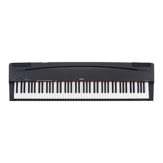
Page 4: Panel Layout
P-70/P-70S PANEL LAYOUT (パネルレイアウト) PHONES スタンバイ / オン q [STANDBY/ON] switch q [STANDBY/ON]スイッチ マスターボリューム w [MASTER VOLUME] slider w [MASTER VOLUME]スライダー デモ / ソング e [DEMO/SONG] button e [DEMO/SONG]ボタン グランドピアノ / ボイス r [GRAND PIANO/VOICE] button r [GRAND PIANO/VOICE]ボタン セレクト... -
Page 5: Circuit Board Layout & Wiring
P-70/P-70S CIRCUIT BOARD LAYOUT & WIRING (ユニットレイアウト&束線図) Upper Case (Inside view) DJACK Speaker(スピーカ) Speaker(スピーカ) Keyboard Assembly (鍵盤Ass'y) Speaker(スピーカ) Speaker(スピーカ) DJACK CN201 CN101 CN201 CN301 CN105 CN104 CN202 CN103 CN401 CN101 CN102 CN301 GHL-H GHL-M GHL-L CONNECTOR REF. No. DESTINATION REMARKS... -
Page 7: Disassembly Procedure
P-70/P-70S DISASSEMBLY PROCEDURE (分解手順) 1. 下ケースAss'y(所要時間: 約12分) Lower Case Assembly (Time Required: about 12 min) 1-1. [S03]のネジ72本を外して、下ケースAss'yを 1-1 Remove the seventy two (72) screws marked [S03]. 外します。(Photo 1) The lower case assembly can then be removed. (Photo 1) Lower Case Assembly [S03] [S03] (下ケースAss'y)... - Page 8 P-70/P-70S 3. AMシート(所要時間: 約13分) AM Circuit Board (Time Required: about 13 min) 3-1 Remove the lower case assembly. (See procedure 1.) 3-1. 下ケースAss'yを外します。 (1項参照) 3-2 Remove the ten (10) screws marked [S01b] . The AM 3-2. [S01b]のネジ10本を外して、AMシートを外し ます。(Photo 2, 4) circuit board can then be removed. (Photo 2, 4) Upper Case Assembly...
- Page 9 P-70/P-70S 6. スピーカ(所要時間: 約14分) Speaker (Time Required: about 14 min) 6-1 Remove the lower case assembly. (See procedure 1.) 6-1. 下ケースAss'yを外します。 (1項参照) 6-2 Remove the two (2) screws marked [U60]. The speaker 6-2. [U60]のネジ2本を外して、SPグリルAss'yを外 します。 (Photo 2, 7) grille assembly can then be removed. (Photo 2, 7) 6-3 Remove the four (4) screws marked [U40] .
- Page 10 P-70/P-70S 8. PNシート(所要時間: 約15分) PN Circuit Board (Time Required: about 15 min) 8-1 Remove the top cover. (See procedure 1.) 8-1. 下ケースAss'yを外します。 (1項参照) 8-2 Remove the six (6) screws marked [S01h]. The PN 8-2. [S01h]のネジ6本を外して、PNシートを外し ます。(Photo 2, 10) circuit board can then be removed. (Photo 2, 10) Upper Case Assembly...
- Page 11 P-70/P-70S Disassembling the Keyboard Assembly 9. GHL (GHS) 鍵盤Ass'yの分解 9-1 White key assembly and black key assembly 白鍵Ass'y、黒鍵Ass'y 9-1 Remove the four (4) screws marked [270A] fixing the 各オクターブ (C〜B) の白鍵Ass'yと黒鍵Ass'yを止 black and white key assembly for one octave (C—B). ...
- Page 12 P-70/P-70S 9-5 Rubber Contact 接点ゴム 9-5 Remove the black and white key assembly for two 該当する接点ゴムの2オクターブ分の白鍵Ass'y/ octaves related to the subject rubber contact. The rubber 黒鍵Ass'yを外して、接点ゴムを外します。 contact can then be removed. (Fig. 4, Fig. 4-1) (図4、図4-1) Note that the rubber contact has a specific installation ※ ...
- Page 13 P-70/P-70S 9-6 GHL88L Circuit Board GHL88Lシート 9-6 Remove the black and white key assembly (A1—B2). A-1〜B2までの白鍵Ass'y/黒鍵Ass'yを外します。 (See procedure 4-1) (4-1項参照) Remove the six (6) screws marked [260A]. The [260A]のネジ6本を外して、GHL88Lシートを外し GHL88L circuit board can then be removed. (Fig. 4) ...
- Page 14 P-70/P-70S 9-9 Hammer (White Key), (Black Key) ハンマー (白鍵) 、 ( 黒鍵) 9-9 Remove the black and white key assembly for the 該当する白鍵Ass y/黒鍵Ass yを外します。 related keys. 鍵盤フレームを裏側にして、後方からハンマーを With the key frame placed upside down, push the ...
- Page 15 P-70/P-70S 10. Assembling the Keyboard Assembly 10. GHL (GHS) 鍵盤Ass'yの組立 10-1 Hammer (White Key), (Black Key) 10-1 ハンマー (白鍵) 、 ( 黒鍵) After applying grease to the bearing section of the ハンマー軸部にグリス塗布後、後方からハンマー (白 hammer, bring the hammer (white key) (black key) ...
- Page 16 P-70/P-70S 10-4 GHL88H Circuit Board 10-4 GHL88Hシート Tighten the five (5) screws marked [260C] to fix the GHL88Hシートを取り付け、[260C]のネジ5本で固 GHL88H circuit board. (Fig. 4) 定します。(図4) 10-5 Rubber Contact 10-5 接点ゴム Note that the rubber contact has s specific installation ...
- Page 17 P-70/P-70S 10-7 White key assembly and black key assembly 10-7 白鍵Ass'y、黒鍵Ass'y After applying grease to the key guide, install the white キーガイドにグリス塗布後、白鍵Ass'y/黒鍵Ass'y key assembly/black key assembly. At this time, check を取り付けます。 to make sure that the key guide of the key frame and ...
-
Page 18: Lsi Pin Description
P-70/P-70S LSI PIN DESCRIPTION ( 端子機能表) YMW767-VTZ (X6055A00) CPU (SWL01B) NAME FUNCTION NAME FUNCTION Ground Ground Input for TEST Power supply +3.3 V TESTN PLLBPN PLL bypass select External memory lower-byte enable / Port F LBN/LWRN/PF6 PLLV PLL Power supply +2.5 V... - Page 19 P-70/P-70S PD789022GB-A15-8E (XZ560100) CPU NAME FUNCTION NAME FUNCTION P32/INTP2/CPT2 Port 3/External interrupt input/Capture edge input Port 1 P31/INTP1 Port 3/External interrupt input P30/INTP0 P47/KR7 P22/RXD/SI0 Port 2/Asynchronous serial interface serial data input/Serial interface serial data input P46/KR6 P21/TXD/SO0 Port 2/Asynchronous serial interface serial data output/Serial interface serial data output...
-
Page 20: Ic Block Diagram
P-70/P-70S IC BLOCK DIAGRAM ( ブロック図) NJM4580E (TE2) (X2331A00) SN74AHCT1G08DCKR (X0158A00) M4580L (XF195A00) Dual Operatinal Amplifier Single 2-Input Positive-AND Gate Dual Operational Amplifier DM: IC402 DM: IC302, 303 AM: IC101-104 +DC Voltage Output A Supply Inverting Output B Input A... -
Page 21: Circuit Boards
P-70/P-70S CIRCUIT BOARDS (シート基板図) AM (X6634D0) ..........22/23 GHL88L (X6244D0) ..........25 DM (X6631C0) ............21 GHL88M (X6245G0) ..........25 DJACK (X6632B0) ..........26 HP (X6632B0) ............25 GHL88H (X6246D0) ..........24 PN (X6632B0) ............26 DM Circuit Board (... - Page 22 P-70/P-70S AM Circuit Board (AMシート) to PN-CN101 to HP-CN301 A’ to Speaker DC IN 12V Components side (部品側) A’ not installed (実装されていません) AM: 2NA-WF20660...
- Page 23 P-70/P-70S AM Circuit Board ( シート) B’ Pattern side (パターン側) B’...
- Page 26 P-70/P-70S DJACK Circuit Board (DJACKシート) MIDI IN PEDAL to DM-CN202 Components side (部品側) PN Circuit Board ( シート) to AM-CN101 to HP-CN301 FUNCTION DEMO/SONG GRAND PIANO/ SELECT VOICE STANDBY/ON MASTER VOLUME Components side (部品側) HP Circuit Board (HPシート) to AM-CN105 Components side (部品側)
-
Page 27: Test Program
P-70/P-70S TEST PROGRAM Preparation ・ Use an AC adaptor PA-5D. ・ Following items are required for testing. (Input impedance of measuring instrument is more than 1M ohm) - Level meter (with JIS-C Filter) - Frequency counter: Below decimal point 3 or more figures measurement is possible. - Page 28 P-70/P-70S Table 1 Test items Test function and judgment criteria Test item ROM version check To check the Master ROM version using C0-A2 keys. Press keys in the specified range and find the key where the sine wave sounds. Check the version by the scale of that key.
- Page 29 P-70/P-70S Test function and judgment criteria Test item Output Level R check Check that the sine wave of 1kHz sounds at the level specified below (DAC input full bit -12 dB). (PAN = R) Connect a level meter (with JIS-C Filter) to the [PHONES] jack for measurement.
- Page 30 P-70/P-70S テストプログラム 1. 準備 ACアダプターは、PA-5Dを使用します。 テストを行うためには、以下の測定器、治具が必要です。(測定器の入力インピーダンスは、1MΩ以上あること。) ・レベルメーター(JIS‐Cフィルター使用) ・周波数カウンター:小数点以下3桁以上測定可能であること。 ・MIDI ケーブル [ MASTER VOLUME ]を最大にして、ペダルはOFFにしておきます。 [ PHONES ]端子に、測定プラグ(ステレオプラグ)を挿入します。( 33 Ω負荷) 2. テストプログラムの起動 [ C#2 ]と[ F2 ]と[ G#2 ]の鍵盤を同時に押さえながら、パワースイッチをON にします。(図1) テストプログラムが正しく起動されると、A3のサイン波が発音されます。 [ DEMO/SONG ]ボタンを押すと、 音が止まります。 (図1) 3. テストの進め方 テスト項目の一覧は、表1のとおりです。 各テストに対応する鍵盤を押すと、テストが実行されます。(図2参照) また、各テスト項目を終了してテスト項目選択状態にする場合、[ DEMO/SONG ]ボタンを押します。 C0 D0 E0 F0 G0 A0...
- Page 31 P-70/P-70S 表1 テスト項目 鍵盤 テスト項目 テスト内容及び判定条件など ROMバージョン確認 C0〜A2の鍵盤でMaster ROMのバージョンを確認します。 指定された範囲の鍵盤を押した時、正弦波が発音される鍵盤の音階でバージ ョンを確認します。(図3参照) 鍵盤C0〜A0を押してMaster ROMのバージョンの整数部を確認します。 鍵盤C1〜A1を押してMaster ROMのバージョンの小数部第1位を確認します。 鍵盤C2〜A2を押してMaster ROMのバージョンの小数部第2位を確認します。 押された鍵盤に対応する数字が現在のバージョンと一致する場合はOK音( C4正弦波)が、一致しない場合はNG音(C2正弦波)が発音されます。 鍵盤と数字の対応は図3を参照してください。 例)Ver. 1. 01の場合 C#0鍵を押した時にC4の正弦波が発音され、 C1鍵を押した時にC4の正弦波が発音され、 C#2鍵を押した時にC4の正弦波が発音されます。 3つのC4正弦波の発音で1. 01が確認できます。 (C#0, C1, C#2以外の鍵盤を押すとC2の正弦波が発音されます) C0 D0 E0 F0 G0 A0 B0 C1 D1 E1 F1 G1 A1 B1 C2 D2 E2 F2 G2 A2...
- Page 32 P-70/P-70S 鍵盤 テスト項目 テスト内容及び判定条件など 出力レベルLチェック 1 kHzの正弦波が下記に指定のレベル(DAC入力フルビット-12 dB)で発音さ れることを確認します。 [ PHONES ] 端子にレベルメーター(JIS- C フィルター使用)を接続して測定 します。 PHONES L: - 7.5 dBu ±2 dB PHONES R: - 50.0 dBu 以下 [ DEMO/SONG ]ボタンでテスト項目を終了する際、発音が止まります。 EQ-LOW周波数チェック 工場検査用のテストです。 EQ-MID周波数チェック 工場検査用のテストです。 EQ-HIGH周波数チェック 工場検査用のテストです。 SWチェック 表2の順番に各スイッチを2個押ししないように押して行きます。各スイッチ を押した時、そのスイッチに対応する音程で(表2参照)正弦波が発音され ます。 すべてのスイッチが正しく押され、 OKとなることを確認します。 指定外のスイッチが押された場合はNGとなります。 スイッチを実際には押しているが、押されたことが検知されない場合は、発 音しないので、NGとします。 OKの場合は、C4の正弦波が発音されます。(1秒間、発音します) NGの場合は、C2の正弦波が発音されます。(NGの場合は何らかの鍵盤を押 すまで発音は止まりません) ペダルチェック テストに入るとC3の正弦波が発音され、ペダルを踏むとC4の正弦波が発音 されます。 ペダルを離すとC4の正弦波の発音が止まり、テストOKとなります。 NGの場合は、正弦波が発音され続けます。(NGの場合は何らかの鍵盤を押 すまで発音は止まりません) MIDIチェック [ MIDI IN ]端子と[ MIDI OUT ]端子をMIDIケーブルで接続後、テストを実行 します。 OKの場合は、C4の正弦波が発音されます。(1秒間、発音します) NGの場合は、C2の正弦波が発音されます。(NGの場合は何らかの鍵盤を押 すまで発音は止まりません)...
-
Page 33: Midi Implementation Chart
P-70/P-70S MIDI IMPLEMENTATION CHART YAMAHA [ Electronic Piano ] Date : 08-APR-2005 Model P-70 MIDI Implementation Chart Version : 1.0 Function Transmitted Recognized Remarks Basic Default 1 - 16 Channel Changed 1 - 16 1 - 16 Mode Default Messages... -
Page 34: Midi インプリメンテーションチャート
P-70/P-70S MIDI インプリメンテーションチャート [電子ピアノ] YAMAHA Date : 08,Apr 2005 Version : 1.0 P-70 MIDIインプリメンテーションチャート ファンクション 送信 受信 備考 1 - 16 ベーシック 電源ON時 1 - 16 1 - 16 チャンネル 設定可能 モード 電源ON時 メッセージ ************** 代用 0 - 127 0 - 127 ノートナンバー ... -
Page 35: Circuit Diagram
ELECTRONIC PIANO P-70/P-70S CIRCUIT DIAGRAM CONTENTS(目次) IC & DIODE OUTSIDE FIGURE(外形図) .......... 2 OVERALL CIRCUIT DIAGRAM(総回路図) DM ....................3 AM ....................4 PN, DJACK, HP................5 GHL88-L, GHL88-M, GHL88-H ............6 Capacitor(コンデンサ) (セ): Ceramic Capacitor(セラミックコンデンサ) (マ): Mylar Capacitor(マイラーコンデンサ) (半セ): Semiconductive Ceramic Capacitor(半導体セラミックコンデンサ)... - Page 36 P-70/P-70S BA33BC0FP (X5889A00) RH5RZ25CA-T1-F (X3679A00) BA50BC0T (X5887A00) REGULATOR +3.3V REGULATOR +5V REGULATOR +5V DM: IC403 DM: IC404 AM: IC401, 402 1. INPUT 1. GND 1. INPUT 2. GND 2. INPUT 2. OUTPUT 3. OUTPUT 3. OUTPUT 3. GND...
- Page 37 DM OVERALL CIRCUIT DIAGRAM (DM P-70/P70S 回路図) (P-70/P-70S) RESET 64M ROM PROG/WAVE REGULATOR +3.3V REGULATOR +2.5V OP AMP to AM-CN103 28CC1-2000004794 DM OVERALL CIRCUIT DIAGRAM (DM 回路図) (P-70/P-70S) to GHL88M...
- Page 38 P-70/P70S AM OVERALL CIRCUIT DIAGRAM (AM 回路図) (P-70/P-70S) POWER AMP to PN-CN101 to Speaker R107, R108, C105 and C106 are not installed.(未実装) OP AMP R207, R208, C205 and C206 are not installed.(未実装) to DM-CN401 to HP-CN301 REGULOTOR +5V DC IN 12V...
- Page 39 PN, DJACK. HP OVERALL CIRCUIT DIAGRAM (PN、DJACK、HP P-70/P70S 回路図) (P-70/P-70S) MASTER VR DEMO/SONG GRAND PIANO/ SELECT VOICE STANDBY/ON 28CC1-2000004795 to AM-CN101 to DM-CN201 DJACK MIDI IN to AM-CN105 MIDI OUT to DM-CN202 C305 is not installed. (未実装) SUSUTAIN PEDAL 28CC1-2000004795 C204 is not installed.
- Page 40 P-70/P70S GHL OVERALL CIRCUIT DIAGRAM (GHL 回路図) (P-70/P-70S) GHL88-L Keyboard Type 28CC1-2000006192 GHL88-M 28CC1-2000006193 to DM-CN301 GHL88-H 28CC1-2000006194 GHL88 OVERALL CIRCUIT DIAGRAM (GHL88 回路図) (P-70/P-70S)
-
Page 41: Parts List
ELECTRONIC PIANO P-70/P-70S PARTS LIST CONTENTS(目次) OVERALL ASSEMBLY(総組立) ..........2 KEYBOARD ASSEMBLY(鍵盤 Ass y) ........4 FOOT PEDAL(フットペダル) ..........6 ELECTRICAL PARTS(電気部品) ........7-13 OPTION(オプション) L-70 KEYBOARD STAND(L-70 スタンド) ......14 L-70S KEYBOARD STAND(L-70S スタンド) ......16 Notes: DESTINATION ABBREVIATIONS... -
Page 42: Overall Assembly(総組立
P-70/P-70S OVERALL ASSEMBLY(総組立) Music Rest 140c 140b 140d 140a... - Page 43 上 ケ ー ス A s s y Upper Case Assembly P-70S (WF08730) ボ タ ン ( A ) WC605700 Button P-70 STANDBY/ON, DEMO/SONG, GRAND PIANO/VOICE, SELECT ボ タ ン ( A ) WF223500 Button A LIGHT GRAY P-70S STANDBY/ON, DEMO/SONG, GRAND PIANO/VOICE, SELECT Dust Proof Cloth 不...
- Page 44 P-70/P-70S KEYBOARD ASSEMBLY(鍵盤 Ass y) Keyboard Assembly (GHL鍵盤Ass'y) GHL88 Circuit 230a Board Assembly (GHL88シー ト) 230d 230b 230d 230c...
- Page 45 REF NO. PART NO. DESCRIPTION QTY RANK G H L 鍵 盤 A s s y KEYBOARD ASSEMBLY P-70/P-70S G H L 鍵 盤 束 線 付 A WF575600 Keyboard Assembly GHL A88 K6 G H L 鍵 盤 A s s...
- Page 46 P-70/P-70S FOOT PEDAL(フットペダル) Connection Diagram White Black REF NO. PART NO. DESCRIPTION 部 品 名 REMARKS QTY RANK FOOT PEDAL フ ッ ト ペ ダ ル P-70/P-70S Foot Pedal IN PLASTIC BAG フ ッ ト ペ ダ ル (VJ07000) AA812880 Pedal Top Cover ペ...
-
Page 47: Electrical Parts(電気部品
P-70S/P-70S ELECTRICAL PARTS(電気部品) 部 品 名 REMARKS REF NO. PART NO. DESCRIPTION QTY RANK 電 気 部 品 ELECTRICAL PARTS P-70/P-70S ∗ A M シ ー ト WF206700 Circuit Board (WF20660)(X6634D0) ∗ D M シ ー ト WF206300 Circuit Board (WF20620)(X6631C0) ∗... - Page 48 P-70/P-70S 部 品 名 REMARKS REF NO. PART NO. DESCRIPTION QTY RANK ケ ミ コ ン C309 V 3 5 0 8 5 0 0 Electrolytic Cap. 100.00 16.0V TP ケ ミ コ ン C310 UR838100 Electrolytic Cap. 100.00 16.0V RX TP ケ...
- Page 49 P-70S/P-70S 部 品 名 REMARKS REF NO. PART NO. DESCRIPTION QTY RANK チ ッ プ 抵 抗 R115 RD355100 Carbon Resistor (chip) 100.0 63M J RECT. チ ッ プ 抵 抗 R117 RD357100 Carbon Resistor (chip) 10.0K 63M J RECT. チ...
- Page 50 P-70/P-70S 部 品 名 REMARKS REF NO. PART NO. DESCRIPTION QTY RANK チ ッ プ セ ラ ( S L ) C206 US062100 Ceramic Capacitor-SL(chip) 100P 50V J RECT. チ ッ プ セ ラ ( S L ) -209 US062100 Ceramic Capacitor-SL(chip) 100P 50V J RECT.
- Page 51 P-70S/P-70S 部 品 名 REMARKS REF NO. PART NO. DESCRIPTION QTY RANK チ ッ プ 抵 抗 R106 RD356100 Carbon Resistor (chip) 1.0K 63M J RECT. チ ッ プ 抵 抗 R107 RD354470 Carbon Resistor (chip) 47.0 63M J RECT. チ...
- Page 52 P-70/P-70S 部 品 名 REMARKS REF NO. PART NO. DESCRIPTION QTY RANK セ ラ コ ン ( B ) C301 FG613100 Ceramic Capacitor-B 1000P 50V K RX TP セ ラ コ ン 2 B C301 VR026200 Ceramic Capacitor-2B 1000P 63V K FORM.
- Page 53 P-70S/P-70S 部 品 名 REMARKS REF NO. PART NO. DESCRIPTION QTY RANK ∗ G H L 8 8 シ ー ト L WF212500 Circuit Board GHL88L (WF46230)(X6244D0) ワ イ ヤ − ト ラ ッ プ WA619500 Wire Trap 52151 17P SE ダ...
- Page 54 L-70/L-70S L-70 KEYBOARD STAND(L-70 スタンド) 140a...
- Page 55 L-70S/L-70S 部 品 名 REMARKS REF NO. PART NO. DESCRIPTION QTY RANK ス タ ン ド KEYBOARD STAND L-70 ∗ ス タ ン ド Keyboard Stand (WF60220) ∗ 側 板 A s s y L WF590200 Side Board LEFT 側...
- Page 56 L-70/L-70S L-70S KEYBOARD STAND(L-70S スタンド) 140a...
- Page 57 L-70S/L-70S 部 品 名 REMARKS REF NO. PART NO. DESCRIPTION QTY RANK ス タ ン ド KEYBOARD STAND L-70S ∗ ス タ ン ド Keyboard Stand (WF60230) ∗ 側 板 A s s y L WF590400 Side Board Assembly LEFT 側...