Table of Contents
Advertisement
Quick Links
SERVICE MANUAL
B MECHANISM
GV-A500 (NTSC)
GV-A500E (PAL)
MICROFILM
GV-A500/A500E
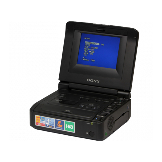
Photo : GV-A500E
SPECIFICATIONS
Canadian Model
Hong Kong Model
For MECHANISM ADJUSTMENT, refer to
the "8mm Video MECHANICAL
ADJUSTMENT MANUAL
VIDEO CASSETTE RECORDER
US Model
GV-A500
AEP Model
UK Model
E Model
GV-A500E
" (9-973-801-11).
Advertisement
Table of Contents

Related Manuals for Sony GV-A500


Summary of Contents for Sony GV-A500
- Page 1 Canadian Model GV-A500 AEP Model UK Model E Model Hong Kong Model GV-A500E B MECHANISM Photo : GV-A500E GV-A500 (NTSC) For MECHANISM ADJUSTMENT, refer to GV-A500E (PAL) the “8mm Video MECHANICAL ADJUSTMENT MANUAL ” (9-973-801-11). SPECIFICATIONS VIDEO CASSETTE RECORDER MICROFILM...
- Page 2 MARK ! ON THE SCHEMATIC DIAGRAMS AND IN THE PARTS CRITIQUES POUR LA SÉCURITÉ DE FONCTIONNEMENT. NE LIST ARE CRITICAL TO SAFE OPERATION. REPLACE THESE REMPLACER CES COMPOSANTS QUE PAR DES PIÈSES SONY COMPONENTS WITH SONY PARTS WHOSE PART NUMBERS DONT LES NUMÉROS SONT DONNÉS DANS CE MANUEL OU APPEAR AS SHOWN IN THIS MANUAL OR IN SUPPLEMENTS DANS LES SUPPÉMENTS PUBLIÉS PAR SONY.
-
Page 3: Table Of Contents
TABLE OF CONTENTS SELF-DIAGNOSIS FUNCTION PRINTED WIRING BOARDS AND Self-diagnosis Function ················································ 5 SCHEMATIC DIAGRAMS Self-diagnosis display ··················································· 5 4-1. FRAME SCHEMATIC DIAGRAM ····························· 4-1 Service Mode Display ·················································· 5 4-2. PRINTED WIRING BOARDS AND 3-1. Display Method ···························································· 5 SCHEMATIC DIAGRAMS ·········································... - Page 4 5-3. VIDEO SECTION ADJUSTMENTS ·························· 5-12 Hue Adjustment for NTSC model (VC-197 baord) ···· 5-42 3-1. PREPARATIONS BEFORE ADJUSTMENT ·············· 5-12 Burst Cleaning Adjustment for PAL model 3-1-1. Equipments to be Used ················································· 5-12 (VC-197 baord) ···························································· 5-43 3-1-2. Precautions in Adjustment ············································ 5-13 Color Adjustment for PAL model (VC-197 baord) ······...
-
Page 5: Self-Diagnosis Function
SELF-DIAGNOSIS FUNCTION 1. Self-diagnosis Function 2. Self-diagnosis display When problems occur while the unit is operating, the self-diagnosis When problems occur while the unit is operating, the counter of the function starts working, and displays on the LCD window what to LCD window shows a 4-digit display consisting of an alphabet and do. -
Page 6: Self-Diagnosis Code Table
4. Self-diagnosis Code Table Self-diagnosis Code Block Detailed Symptom/State Correction Function Code Condensation. Remove the cassette, and insert it again after one hour. Video head is dirty. Clean with the optional cleaning cassette. Non-standard battery is used. Use the InfoLITHIUM battery. LOAD direction. -
Page 18: Disassembly
GV-A500/A500E SECTION 2 DISASSEMBLY NOTE : Follow the disassembly procedure in the numerical order given. 2-1. CASSETTE LID ASSEMBLY 3 Tapping screws Cassette lid assembly Cassette lid assembly 4 Side the eject button 2-2. LCD CABINET 8 Close the LCD panel... -
Page 19: Crystal Indication Module, Fluorescent Cold Cathode Tube
2-3. CRYSTAL INDICATION MODULE, FLUORESCENT COLD CATHODE TUBE, PD-88 BOARD 3 Fixed plate assembly 8 Fluorescent cold cathode tube 9 Crystal indication module 5 PD-88 board Hinge unit Claw of LCD window cabinet assembly... -
Page 20: Cabinet (Bottom) Assembly
2-4. CABINET (BOTTOM) ASSEMBLY 5 M2 screws 5 M2 screws Jack lid 6 Cabinet (bottom) assembly Cabinet (lid) assembly 5 M2 screw 2 Push release button 1 Slightly open LCD panel 2-5. MD BLOCK ASSEMBLY 2-6. CONTROL (FK-71) SWITCH BLOCK, DD-100 BOARD Battery panel assembly... -
Page 21: Board
2-7. VC-197 BOARD 2-8. B MECHANISM DECK 1 M2 screws 1 M2 screw 2 LID frame assembly 4 M2 screws 2 RP shield case 5 VC-197 board 5 B mechanism deck 3 Flexible cables 1 M2 screw 4 Main frame assembly 2 M2 screw 3 M2 screws... -
Page 22: Boards Speaker
2-11. IO-62, IR-29, FP-572, FP-573, FP-574, FP-575 BOARDS SPEAKER 1 Tapping screws !¢ FR-572 7 M2 screw 1 Tapping screws 3 M2 screw 4 IR-29 board 8 FP-575 board ≈ ≈ Jack frame ≈ ≈ 6 FP-574 board assembly 0 IO-62 board 5 M2 screws Remove harness of speaker from... -
Page 23: Circuit Boards Location
2-13.CIRCUIT BOARDS LOCATION PD-88 (LCD DRIVER) DD-100 (POWER SUPPLY) EX-34 (MULTI CONNECTOR) IR-29 (TRANSMITTER) FP-575 (LANC JACK) VC-197 IO-62 (MAIN) (AV IN/OUT) FP-574 (PHONES JACK) 2-6E... -
Page 24: Block Diagrams
GV-A500/A500E SECTION 3 BLOCK DIAGRAMS 3-1. OVERALL BLOCK DIAGRAM VC-197 BOARD EX-34 (SEE PAGE 4-68) (SEE PAGE 4-11,16,19,23,27,30,33,37,41,44,47,51) BOARD EP-51 Q210 T201 (FLEXIBLE) HIGH BL UNREG BACK IC201 LIGHT IC202 DC/DC LCD 4.9V CONV. IC801 DECOD. PANEL FP-569 IC803 V COM... -
Page 25: Video Block Diagram 1
GV-A500/A500E IC129 %£ REC IC129 %£ REC IC129 $§ REC VC-197 BOARD (SEE PAGE 4-19) IC129 $§ REC 0.52Vp-p 0.38Vp-p 0.4Vp-p (NTSC) 0.5Vp-p (PAL) (PAL) (PAL) S JACK IN IC1952 MODE 3-2. VIDEO BLOCK DIAGRAM 1 CONTROL V JACK IN... -
Page 26: Video Block Diagram 2
GV-A500/A500E IC102 @™ REC IC103 @∞ REC IC103 @∞ REC IC101 7 PB IC101 7 PB IC101 5 REC IC101 3 REC IC101 3 REC 0.5Vp-p 0.3Vp-p (NTSC/PAL) 0.4Vp-p 3-3. VIDEO BLOCK DIAGRAM 2 (NTSC) 180msec 0.18Vp-p 190mVp-p (NTSC/PAL) 0.32Vp-p 0.3Vp-p... -
Page 27: Servo Block Diagram
GV-A500/A500E IC121 !• REC/PB 3-4. SERVO BLOCK DIAGRAM IC117 %¶ REC/PB IC117 $¢ REC/PB VC-197 BOARD DD-100 BOARD (SEE PAGE 4-44) IC501 (SEE PAGE 4-75) (2/2) FROM DRUM/CAPSTAN LCD DD ON MODE IC1952 PWM DRIVE CONTROL 3Vp-p VTR DD ON... -
Page 28: System Control Block Diagram
GV-A500/A500E 3-5. SYSTEM CONTROL BLOCK DIAGRAM VC-197 BOARD (SEE PAGE 4-41) IC1952 SYS V IC1952 IC116 IC117 (1/2) D3.2V EEPROM SYSTEM CONTROL 2 SCK TO/FROM 3 DI 37 CS EEPROM VC STBY MODE VC STBY IC1952 CONTROL 4 DO RST VC... -
Page 29: Audio Block Diagram
GV-A500/A500E 3-6. AUDIO BLOCK DIAGRAM VC-197 BOARD (SEE PAGE 4-51) CN207 (SEE PAGE 4-59) BPF MON IC109 REC AFM EX-34 FP-570 CHECK AFM PROCESSOR BOARD (FLEXIBLE) HP L IC361 VIDEO 1 CN109 CN203 CN204 HP/LINE R IC361 BLOCK ADI UNREG... -
Page 30: Mode Control Block Diagram
GV-A500/A500E VC-197 BOARD (SEE PAGE 4-47) IC1952 MODE CONTROL CN001 CN110 KEY AD0 92 KEY AD0 S JACK IN S JACK IN CN107 V JACK IN V JACK IN CN107 3-7. MODE CONTROL BLOCK DIAGRAM S006 S005 S003,004 S002 S001... -
Page 31: Lcd Block Diagram
GV-A500/A500E 3-8. LCD BLOCK DIAGRAM IC801 @º REC/PB PD-88 BOARD IC801 @¢ REC/PB (SEE PAGE 4-68) VC-197 BOARD IC801 3 REC/PB (SEE PAGE 4-33) IC801 CN804 CN801 4.8Vp-p RGB DECODER CN802 4.8Vp-p Q801 Q802 0.5Vp-p -6dB AMP Y IN IC129... -
Page 32: Power Supply Block Diagram
GV-A500/A500E 3-9. POWER SUPPLY BLOCK DIAGRAM DD-100 BOARD FP-576 PD-88 BOARD (SEE PAGE 4-68) (SEE PAGE 4-75) VC-197 BOARD (SEE PAGE 4-11,16,19,23,27,30,33,37,41,44,47,51) BATTERY (FLEXIBLE) TERMINAL CN502 CN106 CN112 CN804 4 INCH BACK CN801 LCD PANEL LIGHT CN501 PS505 L802 BL UNREG... - Page 36 GV-A500/A500E VC-197 BOARD C002 C842 C1160 G-14 C1357 A-18 C1781 D-13 D114 D-20 L1018 C003 C845 C1161 G-14 C1358 C1851 D116 L1019 E-17 C004 C849 C-12 C1162 H-14 C1359 A-18 C1852 D801 C-11 L1020 C005 C850 C-11 C1163 H-15 C1360...
- Page 37 GV-A500/A500E Q1140 R372 A-16 R869 D-11 R1122 F-17 R1320 A-18 R1758 D-14 R1960 H-20 Q1141 G-18 R373 A-15 R871 E-11 R1123 F-17 R1321 D-18 R1759 D-14 R1961 F-20 Q1150 R375 A-15 R872 R1124 E-17 R1322 D-18 R1760 D-14 R1962 G-20...
-
Page 60: Preparations
GV-A500/A500E SECTION 5 ADJUSTMENTS 5-1. PREPARATIONS When performing adjustments, refer to the layout diagrams for adjustment related parts beginning from page 5–46. NTSC model : GV-A500 PAL model : GV-A500E 1-1. PREPARATIONS BEFORE ADJUSTMENT 1-1-1. List of Service Tools • Oscilloscope •... -
Page 61: Using The Adjusting Remote Commander
1-1-2. Adjusting Remote Commander • Changing the address The adjusting remote commander is used for changing the The address increases when the FF ()) button is pressed, calculation coefficient in signal processing, EVR data, etc. The and decreases when the REW (0) button is pressed. There adjusting remote commander performs bidirectional communication are altogether 256 addresses, from 00 to FF. -
Page 62: Page D Address
Note 2 : The ← mark shown in the adjustment data memo column indicates that the address data is fixed and same as the initial value. Adjustment Data Adjustment Data Initial Value Initial Value Address Address Memo Memo GV-A500E GV-A500E GV-A500 GV-A500 AEP,UK E,HK Column AEP,UK E,HK Column ← 00 to 0F ←... -
Page 63: Page F Address
Note 2 : The ← mark shown in the adjustment data memo column indicates that the address data is fixed and same as the initial value. Adjustment Data Adjustment Data Initial Value Initial Value Address Address Memo Memo GV-A500E GV-A500E GV-A500 GV-A500 AEP,UK E,HK Column AEP,UK E,HK Column ← ← ←... - Page 64 Adjustment Data Adjustment Data Initial Value Initial Value Address Address Memo Memo GV-A500E GV-A500E GV-A500 GV-A500 AEP,UK E,HK Column AEP,UK E,HK Column ← ← ← ← ← ← ← ← ← ← ← ← ← ← ← ← ← ←...
- Page 65 Adjustment Data Adjustment Data Initial Value Initial Value Address Address Memo Memo GV-A500E GV-A500E GV-A500 GV-A500 AEP,UK E,HK Column AEP,UK E,HK Column ← ← ← ← ← ← ← ← ← ← ← ← ← ← ← ← ← ←...
-
Page 66: Page E Address
Note 2 : The ← mark shown in the adjustment data memo column indicates that the address data is fixed and same as the initial value. Adjustment Data Adjustment Data Initial Value Initial Value Address Address Memo Memo GV-A500E GV-A500E GV-A500 GV-A500 AEP,UK E,HK Column AEP,UK E,HK Column ← ← ←... - Page 67 1. Initialization of D, E, F Page Data Note 1 : If the D, E, F page data has been initialized, all adjustments need to be performed again. Note 2 : < >: NTSC model: GV-A500 [ ]: PAL model: GV-A500E Initializing method: Adjustment page 1) Set page: 0, address: 01, data: 01.
- Page 68 Note 3 : After changing the data, set page: 0, address: 01, data: 00. Also perform “Modification of E Page Data”. Adjustment Data Adjustment Data Initial Value Initial Value Address Address GV-A500E GV-A500E GV-A500 GV-A500 AEP,UK E,HK AEP,UK E,HK Table 5-1-5.
-
Page 69: Data Processing
Note 3 : After changing the data, set page: 0, address: 01, data: 00. Also perform all adjustments of this unit. Adjustment Data Adjustment Data Initial Value Initial Value Address Address GV-A500E GV-A500E GV-A500 GV-A500 AEP,UK E,HK AEP,UK E,HK Table 5-1-6. 1-3. Data Processing... -
Page 70: Mechanical Section Adjustment
Set page: F, address: 29, data: 01 and press the PAUSE button Playback the alignment tape for tracking. of the adjusting remote commander. WR5-1NP: For NTSC model (GV-A500) Set page: D, address: 10, data: 04 and press the PAUSE button WR5-1CP: For PAL model (GV-A500E) of the adjusting remote commander. -
Page 71: Video Section Adjustments
5-3. VIDEO SECTION ADJUSTMENTS When performing adjustments, refer to the layout diagrams for adjustment related parts beginning from page 5-46. 3-1. PREPARATIONS BEFORE ADJUSTMENT The following adjusting instruments are used for adjusting the video section. 3-1-1. Equipments to be Used TV monitor Oscilloscope: 2 phenomena, band 30 MHz or wider, with delay mode. -
Page 72: Precautions In Adjustment
3-1-2. Precautions in Adjustment The adjustments of this unit are performed in the VTR mode (S VIDEO terminal input or VIDEO terminal input mode). To set to the VTR mode, set the power switch to “ON” or set to the “forced VTR power supply ON mode” (Note 1) using the adjusting remote commander. - Page 73 3-1-4. Connecting the Equipments Connect the measuring instruments as shown in Fig. 5-3-1 according Note 1 : If the VIDEO input is used for adjustments which specify to the input terminal specifications (VIDEO input or S VIDEO for the S VIDEO input to be used, the product input), and perform the adjustments.
-
Page 74: S Video Input
3-1-5. Checking the Input Signals Because the video signal obtained from the pattern generator is the chroma signal terminal of the S VIDEO terminal, and check used as the adjustment signal for adjusting the VTR section, the that the burst signal amplitude of the chroma signal is approximately video output signal must satisfy the given specifications. - Page 75 3-1-6. Alignment Tape The following table lists alignment tapes which are available. Use the tape specified in the signal column for each adjustment. If the type of tape to be used for checking operations is not specified, use whichever type. Record Tape Tape...
- Page 76 Note : Measure using the VIDEO terminal (Terminated at 75 Ω). Fig. 5-3-4. Shows the color bar signals recorded on the alignment tape. For NTSC model White (100%) Cyan White (75%) Green Yellow Magenta Burst signal White 0.714V Blue (75%) 0.286V Black 0.286V...
- Page 77 3-1-7. Input/Output Level and Impedance 3-1-9. Service Mode Video input/output Additional note on adjustment Phono jack, 1 Vp-p, 75Ω, Note : After the completion of the all adjustments, cancel the unbalanced, sync negative service mode by either of the following ways. S video input/output (Hi8 model) 4-pin mini DIN 1) Unplug the main power supply and remove the lithium battery.
-
Page 78: Emg Code (Emergency Code)
2. Emergency Memory Address 2-1. EMG CODE (Emergency Code) When there are no emergency, data 00 will be written in the above The codes shown in the following table which correspond to errors addresses (10 to 1B). When the first emergency occurs, the data that occur are recorded in addresses 10, 14, and 18. -
Page 79: Msw Codes
2-2. MSW Codes • The lower parts of the data of addresses 12, 16 and 1A represent the MSW codes (mode switch, mechanism position) when errors occurs. • The upper parts of the data of addresses 12, 16 and 1A represent, when the mechanism position is to be moved, the MSW codes at the start of movement (when moving the loading motor). - Page 80 3. Bit value discrimination Bit values must be discriminated using the display data of the Display on the Bit values adjustment remote commander for the following items. Us the table adjustment bit3 bit2 bit1 bit0 below to discriminate if the bit value is “1” or “0”. remote commander bit7...
- Page 81 5. Condensation, head clogging check Page 3 Address 17 Function When bit value = 1 When bit value = 0 Condensation state (1 hour preservation) Condensation Head clogging Head clogging Using method: 1) Select page: 3, address: 17. 2) By discriminating the bit value of the display data, the state of the VTR can be discriminated.
-
Page 82: Record Of Use Check
8. VTR state check (3) Page 3 Address 1A Function When bit value = 1 When bit value = 0 Playback tape recording mode Standard 8 Audio mode Monaural Stereo Using method: Select page: 3, address: 1A. By discriminating the bit value of the display data, the state of the VTR can be discriminated. -
Page 83: System Control System Adjustments
3-2. SYSTEM CONTROL SYSTEM ADJUSTMENTS 1. Initialization of D, E, F Page Data If the D, E, F page data is erased due to some reason, perform “1-2. INITIALIZATION OF D, E, F PAGE DATA” (See page 5-8). 2. Battery End Adjustment (VC-197 board) Set the battery end voltage. -
Page 84: Switching Position Adjustment (Vc-197 Board)
Specified Value Adjusting method: Set page: 0, address: 01, data: 01. Note : NTSC model : GV-A500 Change the page: F, address: 3A, data by pressing the PLAY PAL model : GV-A500E and STOP buttons of the remote commander until the duty satifies the specification. -
Page 85: Ntsc Lp Mode Switching Position Adjustment
4) Change the data of page: F, address: 38, and adjust so that the between the measuring point and probe. switching position (t1) becomes the specified value. (Fine Note 2 : NTSC model : GV-A500 adjustment) PAL model : GV-A500E 5) Press the PAUSE button of the adjusting remote commander. - Page 86 2. Filter f0 Adjustment (VC-197 board) 3. Y OUT Level Adjustment (VC-197 board) Minimize the chroma signal residual components during composite Set the Y signal output level. video signal input. Note : Insert the plug into the S video terminal. Note : Do not insert a plug into the S video terminal.
- Page 87 4. C OUT Level Adjustment (VC-197 board) 5. RP Filter f0 Adjustment (VC-197 board) Set the chroma signal output level. Adjust the LPF of the playback RF amplifier. Note : Insert the plug into the S video terminal. Mode VTR stop Subject Arbitrary Mode...
- Page 88 6. AFC f0 Adjustment (VC-197 board) Adjust the pull-in range of the A/D converted clock generator during playback. Note : Do not insert the plug in the S video terminal. Mode VTR stop Signal Color bar (Video input) Pin !§ of CN207 (AFC f0) Measurement Point Measuring Instrument Digital voltmeter...
- Page 89 7. NTSC Hi8 REC Y Current Adjustment (VC-197 board) 8. PAL Hi8 REC Y Current Adjustment (VC-197 board) Adjust the Y FM signal recording current. Adjust the Y FM signal recording current. Mode VTR recording Mode VTR recording (SP mode) Signal No signal Signal...
-
Page 90: (Vc-197 Board)
9. NTSC Hi8 REC C Current Adjustment (VC-197 board) Set the recording levels of the REC AFM signal and REC ATF signal. Note : Do not insert a plug into the AUDIO (R) terminal. If the level is too low, the audio S/N will deteriorate, tracking will not be stable, or SP/LP will not be discriminated properly. -
Page 91: (Vc-197 Board)
10. PAL Hi8 REC C Current Adjustment (VC-197 board) Set the recording levels of the REC AFM signal and REC ATF signal. Note : Do not insert a plug into the AUDIO (R) terminal. If the level is too low, the audio S/N will deteriorate, tracking will not be stable, or SP/LP will not be discriminated properly. -
Page 92: (Vc-197 Board)
11. REC C Current Adjustment (VC-197 board) Set the recording current level of REC chroma signal. If it is lower than its normal level, chroma signal noise in played back picture will increase and white modulation noises will be produced. Mode VTR recording (SP mode) Signal... -
Page 93: Ir Transmitter Adjustments
3-5. IR Transmitter Adjustments Adjust using a IR receiver jig. Switch setting: LASER LINK ················································ ON (Red LED is lit) 2. IR Video Deviation Adjustment (MI-27/28 board) 1. IR Video Carrier Frequency Adjustment (MI-27/28 board) Mode VTR stop Mode VTR stop Subject Arbitrary Subject... -
Page 94: Ir Audio Deviation Adjustment (Mi-27/28 Board)
3. IR Audio Deviation Adjustment (MI-27/28 board) Mode VTR recording Signal Audio signal: 400 Hz, –7.5 dBs: Left or right of audio input/output terminal Video signal: Color bar signal: Video input/ output terminal Measuring point AUDIO OUT L terminal and AUDIO OUT R terminal of IR receiver jig (Terminated at 47 kΩ) Measuring instrument... -
Page 95: Audio System Adjustment
3-6. AUDIO SYSTEM ADJUSTMENT [Connecting the measuring instruments for the audio] • Perform the adjustment using the color bar signal as a video Connect the audio system measuring instruments in addition to the signal input for VIDEO terminal. video system measuring instruments as shown in Fig. 5-3-25, and •... -
Page 96: Mhz Deviation Adjustment (Vc-197 Board)
S2 ············· NT position (NTSC) PAL position (PAL) PAL position (PAL) S3 ············· SIN position S3 ············· SIN position Note : NTSC model : GV-A500 Note : NTSC model : GV-A500 PAL model : GV-A500E PAL model : GV-A500E Adjustment method:... -
Page 97: Bpf F0 Adjustment (Vc-197 Board)
Specified value The Main and Sub channel distortion rates should be almost the same (within ± 1%) and minimum Note : NTSC model : GV-A500 PAL model : GV-A500E Adjustment method: 1) Set page: 0, address: 01, data: 01. 2) Set the Hi-Fi sound switch (menu display) to “ 2 ”. -
Page 98: Lcd System Adjustment
Check that the input signal level is 1.00 Vp-p before adjusting. Fixed value Fixed value 100IRE Fixed value (Fixed value) Fixed value Approx. 0.714V Fixed value 1.00V Fixed value Fixed value Approx. ( ): NTSC model only (GV-A500) 0.286V Horizontal sync Fig. 5-3-27. 5-39... -
Page 99: Vco Adjustment (Pd-88 Baord)
2. VCO Adjustment (PD-88 baord) 3. H POS Adjustment (VC-197 baord) Set the VCO freerun frequency. If deviated, the LCD screen will be Adjusts the horizontal position of picture on LCD display. blurred. Mode VTR stop Mode VTR stop Signal Color bar signal Signal No signal... -
Page 100: Bright Adjustment (Vc-197 Baord)
4. Bright Adjustment (VC-197 baord) 5. Contrast Adjustment (VC-197 baord) Set the D range of the RGB decoder used to drive the LCD to the Set the level of the VIDEO signal for driving the LCD to the specified specified value. If deviated, the LCD screen will become blackish value. -
Page 101: Color Adjustment For Ntsc Model (Vc-197 Baord)
6. Color Adjustment for NTSC model (VC-197 baord) 7. Hue Adjustment for NTSC model (VC-197 baord) Set the color saturation to the standard value. If deviated, the color Set the hue to the standard value. If deviated, the color will be to will be to dark or light. - Page 102 8. Burst Cleaning Adjustment for PAL model 9. Color Adjustment for PAL model (VC-197 baord) (VC-197 baord) Set the color saturation to the standard value. If deviated, the color Adjust to the optimum PAL chroma signal demodulation phase. If will be to dark or light. the phase is not correct, moire distortion noises will stand out.
- Page 103 10. V-COM Adjustment (PD-88 baord) 11. White Balance Adjustment (VC-197 baord) Set the DC bias of the common electrode drive signal of LCD display Correct the white balance. to the specified value. If deviated, the LCD screen color cannot be reproduced. If deviated, the LCD display will move, producing flicker and conspicuous vertical lines.
- Page 104 GV-A500/A500E SECTION 6 REPAIR PARTS LIST 6-1. EXPLODED VIEWS Note: • -XX, -X mean standardized parts, so they may • The mechanical parts with no reference number have some differences from the original one. in the exploded views are not supplied.
- Page 105 6-1-2. LCD BLOCK, UPPER CABINET BLOCK ASSEMBLY The components identified by Les composants identifiés par mark ! or dotted line with mark une marque ! sont critiques ! are critical for safety. pour la sécurité. Replace only with part number Ne les remplacer que par une specified.
- Page 106 6-1-3. MD BLOCK ASSEMBLY not supplied Ref. No. Part No. Description Remarks Ref. No. Part No. Description Remarks 3-968-729-51 SCREW (M2), LOCK ACE, P2 3-978-713-01 SPRING (R), FRAME RETURN 1-667-402-11 FP-573 FLEXIBLE BOARD 3-703-816-33 SCREW (M1.4X1.6), SPECIAL HEAD A-7085-076-A VC-197 BOARD, COMPLETE (A500) 1-475-383-31 SWITCH BLOCK, CONTROL (FK-71) A-7085-077-A VC-197 BOARD, COMPLETE (A500E) 3-978-711-01 LID, LOADING...
- Page 107 6-1-4. CASSETTE COMPARTMENT BLOCK SECTION LS CHASSIS BLOCK SECTION (See page 6-5) MECHANISM CHASSIS BLOCK SECTION (See page 6-6) Ref. No. Part No. Description Remarks Ref. No. Part No. Description Remarks A-7040-421-A DAMPER ASSY X-3945-399-1 GEAR ASSY, GOOSENECK 7-624-102-04 STOP RING 1.5, TYPE -E 3-947-503-01 SCREW (M1.4X2.5) X-3945-400-1 CASSETTE COMPARTMENT ASSY 3-727-176-01 WASHER...
- Page 108 6-1-5. LS CHASSIS BLOCK SECTION S002 D001 FP-249 (not supplied) Ref. No. Part No. Description Remarks Ref. No. Part No. Description Remarks A-7040-419-A BASE (S) BLOCK ASSY, GUIDE 3-965-648-01 SPRING (PINCH), TENSION A-7040-418-B BASE (T) BLOCK ASSY, GUIDE 3-965-579-01 ROLLER, PINCH PRESS 3-965-559-01 STOPPER (T) 3-965-563-01 GEAR, T SOFT 3-965-557-01 STOPPER (T), GB...
- Page 109 6-1-6. MECHANISM CHASSIS BLOCK SECTION M901 81 1 M903 M902 S901 Ref. No. Part No. Description Remarks Ref. No. Part No. Description Remarks X-3947-343-1 GROUND (IM) ASSY, SHAFT 3-965-535-01 SPRING, TENSION 3-965-550-02 SCREW (M1.7X1.6) 3-965-542-01 SHIELD, MOTOR 1-657-785-11 FP-248 FLEXIBLE BOARD 3-965-539-01 GEAR (A) 3-965-545-01 SPACER, CAPSTAN 3-965-538-01 SLEEVE, MOTOR HOLDER...
- Page 110 DD-100 6-2. ELECTRICAL PARTS LIST Note: • Items marked “*” are not stocked since they • COILS When indicating parts by reference number, are seldom required for routine service. Some uH: µH please include the board name. delay should be anticipated when ordering these •...
- Page 111 DD-100 EX-34 FP-249 FP-355 FP-571 Ref. No. Part No. Description Remarks Ref. No. Part No. Description Remarks L516 1-414-396-21 INDUCTOR 4.7uH R542 1-216-821-11 METAL CHIP 1/16W L517 1-414-404-11 INDUCTOR 100uH R548 1-216-295-11 CONDUCTOR, CHIP (2012) L518 1-414-404-11 INDUCTOR 100uH R549 1-216-295-11 CONDUCTOR, CHIP (2012) L519 1-412-054-21 INDUCTOR CHIP 2.2uH...
- Page 112 D106 8-719-062-16 DIODE 01ZA8.2(TPL3) S107 1-771-025-21 SWITCH, ROTARY (ENCODER) D107 8-719-062-16 DIODE 01ZA8.2(TPL3) D108 8-719-420-14 DIODE MA8082-TX D109 8-719-061-82 DIODE TLSU1002(TPX1,SONY) A-7073-329-A IR-29 BOARD, COMPLETE D110 8-719-062-16 DIODE 01ZA8.2(TPL3) ********************** (Ref.No.: 3,000 Series) D111 8-719-420-14 DIODE MA8082-M D112 8-719-420-14 DIODE MA8082-M <...
- Page 113 IR-29 PD-88 Ref. No. Part No. Description Remarks Ref. No. Part No. Description Remarks < CONNECTOR > C828 1-164-664-11 CERAMIC CHIP 0.033uF ! C830 1-113-521-11 CERAMIC CHIP 12PF CN361 1-766-866-21 CONNECTOR, FFC/FPC 6P C831 1-165-319-11 CERAMIC CHIP 0.1uF C832 1-104-913-11 TANTAL. CHIP 10uF <...
- Page 114 PD-88 VC-197 Ref. No. Part No. Description Remarks Ref. No. Part No. Description Remarks R814 1-216-833-11 METAL CHIP 1/16W C013 1-107-826-11 CERAMIC CHIP 0.1uF R815 1-216-829-11 METAL CHIP 4.7K 1/16W C014 1-135-259-11 TANTAL. CHIP 10uF 6.3V R816 1-218-873-11 METAL GLAZE 0.50% 1/16W C015 1-164-346-11 CERAMIC CHIP...
- Page 115 VC-197 Ref. No. Part No. Description Remarks Ref. No. Part No. Description Remarks C713 1-164-004-11 CERAMIC CHIP 0.1uF C1012 1-164-217-11 CERAMIC CHIP 150PF C714 1-162-964-11 CERAMIC CHIP 0.001uF C1013 1-162-927-11 CERAMIC CHIP 100PF C715 1-164-156-11 CERAMIC CHIP 0.1uF C1014 1-162-926-11 CERAMIC CHIP 82PF C719 1-162-970-11 CERAMIC CHIP...
- Page 116 VC-197 Ref. No. Part No. Description Remarks Ref. No. Part No. Description Remarks C1076 1-162-967-11 CERAMIC CHIP 0.0033uF 10% C1213 1-135-201-11 TANTALUM CHIP 10uF C1077 1-162-958-11 CERAMIC CHIP 270PF C1215 1-135-201-11 TANTALUM CHIP 10uF C1078 1-162-908-11 CERAMIC CHIP 0.25PF 50V C1216 1-162-970-11 CERAMIC CHIP 0.01uF...
- Page 117 VC-197 Ref. No. Part No. Description Remarks Ref. No. Part No. Description Remarks C1341 1-162-920-11 CERAMIC CHIP 27PF C1453 1-162-966-11 CERAMIC CHIP 0.0022uF 10% C1342 1-162-928-11 CERAMIC CHIP 120PF C1463 1-135-201-11 TANTALUM CHIP 10uF (A500E) C1465 1-115-467-11 CERAMIC CHIP 0.22uF C1342 1-164-217-11 CERAMIC CHIP 150PF...
- Page 118 VC-197 Ref. No. Part No. Description Remarks Ref. No. Part No. Description Remarks C1854 1-162-968-11 CERAMIC CHIP 0.0047uF 10% C1992 1-162-970-11 CERAMIC CHIP 0.01uF C1855 1-107-826-11 CERAMIC CHIP 0.1uF C1856 1-162-968-11 CERAMIC CHIP 0.0047uF 10% < CONNECTOR > C1857 1-162-968-11 CERAMIC CHIP 0.0047uF 10% C1858 1-107-826-11 CERAMIC CHIP...
- Page 119 VC-197 Ref. No. Part No. Description Remarks Ref. No. Part No. Description Remarks < IC > L1004 1-414-406-11 INDUCTOR 220uH L1005 1-414-398-11 INDUCTOR 10uH IC001 8-759-456-30 IC BA7787FS-E2 L1006 1-412-948-11 INDUCTOR 5.6uH IC101 8-752-070-64 IC CXA1702AR L1007 1-410-656-11 INDUCTOR CHIP 150uH IC102 8-759-447-79 IC MB87B121PFV-G-BND-E L1008...
- Page 120 VC-197 Ref. No. Part No. Description Remarks Ref. No. Part No. Description Remarks Q353 8-729-037-53 TRANSISTOR 2SB1462J-QR(TX).SO Q1221 8-729-037-74 TRANSISTOR UN9213J-(TX).SO Q701 8-729-037-52 TRANSISTOR 2SD2216J-QR(TX).SO Q1305 8-729-037-52 TRANSISTOR 2SD2216J-QR(TX).SO Q702 8-729-037-52 TRANSISTOR 2SD2216J-QR(TX).SO Q1306 8-729-037-52 TRANSISTOR 2SD2216J-QR(TX).SO Q703 8-729-037-52 TRANSISTOR 2SD2216J-QR(TX).SO Q1307 8-729-037-53 TRANSISTOR 2SB1462J-QR(TX).SO Q704...
- Page 121 VC-197 Ref. No. Part No. Description Remarks Ref. No. Part No. Description Remarks R012 1-202-924-11 METAL GLAZE 1/16W R706 1-216-845-11 METAL CHIP 100K 1/16W R015 1-216-809-11 METAL CHIP 1/16W (A500) R016 1-216-809-11 METAL CHIP 1/16W R707 1-216-824-11 METAL CHIP 1.8K 1/16W R017 1-216-821-11 METAL CHIP...
- Page 122 VC-197 Ref. No. Part No. Description Remarks Ref. No. Part No. Description Remarks R833 1-216-843-11 METAL CHIP 1/16W R902 1-216-864-11 METAL CHIP 1/16W (A500E) R904 1-216-864-11 METAL CHIP 1/16W R834 1-216-864-11 METAL CHIP 1/16W R1001 1-216-818-11 METAL CHIP 1/16W R835 1-216-838-11 METAL CHIP 1/16W R1002...
- Page 123 VC-197 Ref. No. Part No. Description Remarks Ref. No. Part No. Description Remarks R1048 1-216-832-11 METAL CHIP 8.2K 1/16W R1119 1-216-833-11 METAL CHIP 1/16W (A500E) R1120 1-216-817-11 METAL CHIP 1/16W R1051 1-216-835-11 METAL CHIP 1/16W R1121 1-216-817-11 METAL CHIP 1/16W (A500E) R1122 1-216-839-11 METAL CHIP...
- Page 124 VC-197 Ref. No. Part No. Description Remarks Ref. No. Part No. Description Remarks R1221 1-216-818-11 METAL CHIP 1/16W R1320 1-216-815-11 METAL CHIP 1/16W R1222 1-216-820-11 METAL CHIP 1/16W R1321 1-218-876-11 METAL GLAZE 0.50% 1/16W R1223 1-216-821-11 METAL CHIP 1/16W R1322 1-218-847-11 METAL GLAZE 0.50% 1/16W R1225...
- Page 125 VC-197 Ref. No. Part No. Description Remarks Ref. No. Part No. Description Remarks R1389 1-216-833-11 METAL CHIP 1/16W R1774 1-218-847-11 METAL GLAZE 0.50% 1/16W R1403 1-216-844-11 METAL CHIP 1/16W R1775 1-216-841-11 METAL CHIP 1/16W R1404 1-216-853-11 METAL CHIP 470K 1/16W R1776 1-216-821-11 METAL CHIP 1/16W...
- Page 126 VC-197 Ref. No. Part No. Description Remarks Ref. No. Part No. Description Remarks R1865 1-216-851-11 METAL CHIP 330K 1/16W R1977 1-216-853-11 METAL CHIP 470K 1/16W R1866 1-216-853-11 METAL CHIP 470K 1/16W R1978 1-216-821-11 METAL CHIP 1/16W R1867 1-216-845-11 METAL CHIP 100K 1/16W R1979...
- Page 127 VC-197 Ref. No. Part No. Description Remarks Ref. No. Part No. Description Remarks < VIBRATOR > ACCESSORIES & PACKING MATERIALS ******************************* X801 1-579-466-11 VIBRATOR, CRYSTAL 3.579545MHz (A500) X801 1-579-661-21 OSCILLATOR, CRYSTAL 4.43619MHz(A500E) ! A-7009-474-F POWER ADAPTER AC-V615 (A500) X1305 1-767-028-21 VIBRATOR, CRYSTAL 14.318182MHz (A500) ! A-7009-475-A POWER ADAPTER AC-V615 (A500E) X1305 1-767-029-21 VIBRATOR, CRYSTAL 17.734475MHz (A500E)