Table of Contents
Advertisement
SERVICE MANUAL
Ver. 1.2 2010.03
• HCD-DZ280/DZ680/HDZ284/HDZ485 are the amplifi er, DVD/CD
and tuner section in DAV-DZ280/DZ680/HDZ284/HDZ485.
This system incorporates with Dolby* Digital and Dolby Pro
Logic (II) adaptive matrix surround decoder and the DTS** Digital
Surround System.
* Manufactured under license from Dolby Laboratories.
Dolby, Pro Logic, and the double-D symbol are trademarks of
Dolby Laboratories.
** Manufactured under license under U.S. Patent #'s:
5,451,942; 5,956,674; 5,974,380; 5,978,762; 6,487,535 & other
U.S. and worldwide patents issued & pending. DTS and DTS
Digital Surround are registered trademarks and the DTS logos
and Symbol are trademarks of DTS, Inc. © 1996-2008 DTS,
Inc. All Rights Reserved.
Amplifi er Section
Stereo mode (rated)
108 W + 108 W (at 3 ohms,
1 kHz, 1% THD)
DZ280/DZ680/HDZ284:
Surround mode (reference) RMS output power
FL/FR/C/SL/SR*: 142
watts (per channel at 3
ohms, 1 kHz, 10% THD)
Subwoofer*: 140 watts (at
3 ohms, 80 Hz, 10% THD)
HDZ485:
Surround mode (reference) RMS output power
FL/FR/C/SL/SR*: 144
watts (per channel at 3
ohms, 1 kHz, 10% THD)
Subwoofer*: 280 watts (at
1.5 ohms, 80 Hz, 10% THD)
* Depending on the decoding mode settings and the
source, there may be no sound output.
Inputs (Analog) (DZ280/DZ680)
TV (AUDIO IN)
Sensitivity: 450/250 mV
AUDIO IN
Sensitivity: 250/125 mV
Inputs (Digital) (DZ680/HDZ284/HDZ485)
TV/VIDEO (COAXIAL IN/OPTICAL IN)
Impedance: 75 ohms/-
Input Stream: Dolby
Digital 5.1ch/DTS 5.1ch/
Linear PCM 2ch
(Sampling Frequency: less
than 48 kHz)
Sony Corporation
9-889-391-03
2010C04-1
Audio&Video Business Group
©
2010.03
Published by Sony Techno Create Corporation
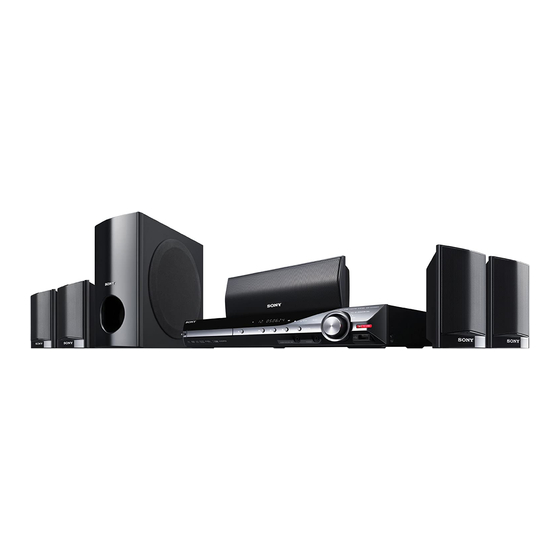
Photo: HCD-HDZ284
Model Name Using Similar Mechanism
Mechanism Type
Optical Pick-up Name
SPECIFICATIONS
Inputs (Analog) (HDZ284/HDZ485)
TV/VIDEO (AUDIO IN) Sensitivity: 450/250 mV
AUDIO IN
Sensitivity: 250/125 mV
Outputs (Analog)
Phones
Accepts low- and high-
impedance headphones.
Super Audio CD/DVD System
Laser Diode Properties
Emission Duration:
Continuous
Laser Output: Less than
44.6μW
* This output is the value measurement at a distance
of 200mm from the objective lens surface on the
Optical Pick-up Block with 7mm aperture.
Signal format system
HDZ284/HDZ485:
NTSC
DZ280/DZ680:
NTSC/PAL
USB Section (DZ280/DZ680)
(USB) port:
Maximum current:
500 mA
Tuner Section
System
PLL quartz-locked digital
synthesizer
FM Tuner section
Tuning range
Canadian, PX models:
87.5 MHz - 108.0 MHz
(100 kHz step)
HCD-DZ280/DZ680/
HDZ284/HDZ485
Canadian Model
HCD-HDZ284/HDZ485
HCD-DZ260/DZ270/HDZ278
CDM85-DVBU102
KHM-313CAA
Other models:
Antenna (aerial)
Antenna (aerial) terminals 75 ohms, unbalanced
Intermediate frequency
Video Section (DZ280/DZ680)
Outputs
Video Section (HDZ284/HDZ485)
Outputs
– Continued on next page –
DVD RECEIVER
AEP Model
UK Model
HCD-DZ280/DZ680
PX Model
HCD-HDZ485
87.5 MHz - 108.0 MHz
(50 kHz step)
FM wire antenna (aerial)
10.7 MHz
VIDEO: 1 Vp-p 75 ohms
R/G/B: 0.7 Vp-p 75 ohms
HDMI OUT: Type A (19
pin)
VIDEO: 1 Vp-p 75 ohms
COMPONENT:
Y: 1 Vp-p 75 ohms
P
/C
, P
/C
: 0.7 Vp-p
B
B
R
R
75 ohms
HDMI OUT: Type A (19
pin)
Advertisement
Table of Contents

Related Manuals for Sony HCD-DZ280


Summary of Contents for Sony HCD-DZ280
- Page 1 HCD-DZ280/DZ680 Ver. 1.2 2010.03 PX Model HCD-HDZ485 Photo: HCD-HDZ284 • HCD-DZ280/DZ680/HDZ284/HDZ485 are the amplifi er, DVD/CD and tuner section in DAV-DZ280/DZ680/HDZ284/HDZ485. This system incorporates with Dolby* Digital and Dolby Pro Model Name Using Similar Mechanism HCD-DZ260/DZ270/HDZ278 Logic (II) adaptive matrix surround decoder and the DTS** Digital...
- Page 2 LES DIAGRAMMES SCHÉMATIQUES ET LA LISTE DES PIÈCES SONT CRITIQUES POUR LA SÉCURITÉ DE FONC- TIONNEMENT. NE REMPLACER CES COMPOSANTS QUE PAR DES PIÈCES SONY DONT LES NUMÉROS SONT DON- NÉS DANS CE MANUEL OU DANS LES SUPPLÉMENTS PUBLIÉS PAR SONY.
- Page 3 HCD-DZ280/DZ680/HDZ284/HDZ485 Ver. 1.1 MODEL IDENTIFICATION SAFETY CHECK-OUT – Back Panel – After correcting the original service problem, perform the follow- ing safety check before releasing the set to the customer: Check the antenna terminals, metal trim, “metallized” knobs, screws, and all other exposed metal parts for AC leakage.
- Page 4 HCD-DZ280/DZ680/HDZ284/HDZ485 Laser component in this product is capable of emitting radiation exceeding the limit for Class 1. This appliance is classifi ed as a CLASS 1 LASER product. This marking is located on the rear or bottom exterior. CAUTION Use of controls or adjustments or performance of procedures other than those specifi...
- Page 5 HCD-DZ280/DZ680/HDZ284/HDZ485 Playable Discs • • DVD-R/DVD-RW in DVD VIDEO format or video mode • DVD+R/DVD+RW in DVD VIDEO format VR (Video • DVD-R/DVD-RW in VR (Video Recording) mode Recording) mode (except for DVD-R • • Super VCD • CD-R/CD-RW/CD-ROM in video CD format or Super VCD format •...
- Page 6 HCD-DZ280/DZ680/HDZ284/HDZ485 A logical format of files and folders on CD-ROMs, defined by ISO (International Organization for Standardization). Notes on discs This product is designed to playback discs that conform to the Compact Disc (CD) standard. DualDiscs and some of the music discs encoded with copyright protection technologies do not conform to the Compact Disc (CD) standard, therefore, these discs may not be playable by this product.
- Page 7 HCD-DZ280/DZ680/HDZ284/HDZ485 Region code Your system has a region code printed on the rear of the unit and will only play a DVD labeled with the same region code. A DVD VIDEO labeled will also play on this system. If you try to play any other DVD VIDEO, the message [Playback prohibited by area limitations.] will appear on the TV screen.
- Page 8 [VER.X.XX] (X is a number) may display) appear on the TV screen. Although this is not a malfunction and for Sony service use only, When the self-diagnosis function is activated to normal system operation will not be possible. prevent the system from malfunctioning, a 5- Turn off the system, and then turn on the system character service number (e.g., C 13 50) with a...
-
Page 9: Table Of Contents
HCD-DZ280/DZ680/HDZ284/HDZ485 TABLE OF CONTENTS SERVICING NOTES 6-11. Schematic Diagram –MAIN Section (4/10)– ....43 ..........10 6-12. Schematic Diagram –MAIN Section (5/10)– ....44 6-13. Schematic Diagram –MAIN Section (6/10)– ....45 GENERAL ..............12 6-14. Schematic Diagram –MAIN Section (7/10)– ....46 6-15. -
Page 10: Servicing Notes
HCD-DZ280/DZ680/HDZ284/HDZ485 SECTION 1 SERVICING NOTES How to open the disc table when power switch turns off NOTES ON HANDLING THE OPTICAL PICK-UP Insert a tapering driver into the aperture of the unit bottom, and BLOCK OR BASE UNIT slide it in the direction of the arrow. - Page 11 HCD-DZ280/DZ680/HDZ284/HDZ485 Discharge the charged electricity in capacitors to prevent electric shock as follows When disassembling the machine, be sure to discharge the charged electricity in the following capacitors. Use a resistor of 800 ohms, 2 Watts for discharging the following capacitors.
-
Page 12: General
HCD-DZ280/DZ680/HDZ284/HDZ485 SECTION 2 GENERAL This section is extracted from instruction manual. Rear panel Index to Parts and Control (DZ280) For more information, refer to the pages indicated in parentheses. Front panel ANTENNA SPEAKER FRONT R FRONT L SUR R SUR L... - Page 13 HCD-DZ280/DZ680/HDZ284/HDZ485 Rear panel Index to Parts and Control (DZ680) For more information, refer to the pages indicated in parentheses. Screws* Front panel ANTENNA SPEAKER FRONT R FRONT L SUR R SUR L COAXIAL 75 EZW-T100 EURO AV SPEAKER HDMI OUT...
- Page 14 HCD-DZ280/DZ680/HDZ284/HDZ485 Rear panel Index to Parts and Control (HDZ284) For more information, refer to the pages indicated in parentheses. Front panel ANTENNA SPEAKER FRONT R FRONT L SUR R SUR L COAXIAL 75 TV/VIDEO SPEAKER HDMI OUT DIGITAL IN DMPORT...
- Page 15 HCD-DZ280/DZ680/HDZ284/HDZ485 Rear panel Index to Parts and Control (HDZ485) For more information, refer to the pages indicated in parentheses. Screws* Front panel ANTENNA SPEAKER FRONT R FRONT L SUR R SUR L COAXIAL 75 EZW-T100 TV/VIDEO SPEAKER HDMI OUT DIGITAL IN...
-
Page 16: Disassembly
HCD-DZ280/DZ680/HDZ284/HDZ485 SECTION 3 DISASSEMBLY • This set can be disassembled in the order shown below. 3-1. CASE (Page 17) 3-2. FRONT PANEL SECTION (Page 17) 3-3. BACK PANEL SECTION 3-4. BACK PANEL SECTION (DZ680/HDZ485) (DZ280/HDZ284) (Page 18) (Page 18) 3-5. -
Page 17: Case
HCD-DZ280/DZ680/HDZ284/HDZ485 Note: Follow the disassembly procedure in the numerical order given. 3-1. CASE case two screws (case 3 TP2) five screws (BV/ring) two screws (case 3 TP2) 3-2. FRONT PANEL SECTION CN4014 (4P) wire (flat type)(17 core) (CN506) CN3001 (3P) -
Page 18: Back Panel Section (Dz680/Hdz485)
HCD-DZ280/DZ680/HDZ284/HDZ485 3-3. BACK PANEL SECTION (DZ680/HDZ485) two screws (+BVTP 3 × 8) back panel section three screws screw (+BVTP 3 × 8) (+BVTP 3 × 8) wire (flat type) (11 core) (CN4017) (DZ680) screw wire (flat type) (9 core) (CN4016) (+B 3 ×... -
Page 19: Dvd Mechanism Deck
HCD-DZ280/DZ680/HDZ284/HDZ485 3-5. DVD MECHANISM DECK screw screw (+BV3 (3-CR)) (+BV3 (3-CR)) cover (CDM-DSY) screw (+BV3 (3-CR)) two screws screw (+BV3 (3-CR)) (+BV3 (3-CR)) wire (flat type)(5 core) (CN1202) CN1201 (6P) DVD mechanism deck wire (flat type)(24 core) (CN1101) 3-6. POWER BOARD, USB BOARD (DZ280/DZ680) -
Page 20: Main Board, Speaker Board
HCD-DZ280/DZ680/HDZ284/HDZ485 3-7. MAIN BOARD, SPEAKER BOARD wire (flat type) (17 core) (CN472) three screws (HDZ284/HDZ485) (+BV3 (3-CR)) wire (flat type) (19 core) (CN473) (DZ280/DZ680) heat sink section wire (flat type) (5 core) (CN303) radiation (HDZ485) wire (flat type) (17 core) (CN503) -
Page 21: Tray
HCD-DZ280/DZ680/HDZ284/HDZ485 3-9. TRAY Move the chuck cam in the direction of the arrow. bottom side two claws tray 3-10. BELT chuck cam belt two claws... -
Page 22: Board
HCD-DZ280/DZ680/HDZ284/HDZ485 3-11. MS-203 BOARD MS-203 board DC motor three claws screw (M 1.7 × 2.5) 3-12. BASE UNIT two claws chuck cam two claws base unit... -
Page 23: Optical Pick-Up
HCD-DZ280/DZ680/HDZ284/HDZ485 3-13. OPTICAL PICK-UP FFC holder two insulator screws two insulator screws two insulators optical pick-up (KHM-313CAA) two insulators two claws... -
Page 24: Test Mode
HCD-DZ280/DZ680/HDZ284/HDZ485 SECTION 4 TEST MODE 2-4. Key Test Mode Note: Incorrect operations may be performed if the test mode is not Procedure: entered properly. 1. When the display test mode is activated, press the [ ] button, In this case, press the [?/1] button to turn the power off, and to select the key test mode. - Page 25 HCD-DZ280/DZ680/HDZ284/HDZ485 5. Product Out DVD SECTION • This mode moves the optical pick-up to the position durable 6-1. GENERAL DESCRIPTION to vibration and clears all data including preset data stored in • The IOP measurement allows you to make diagnosis and ad- the RAM to initial conditions.
- Page 26 HCD-DZ280/DZ680/HDZ284/HDZ485 (2) Select “2. Drive Manual Operation” by pressing the [2] button 6-4. EMERGENCY HISTORY on the remote commander. The screen will appear as shown. To check the emergency history, please follow the following procedure. Drive Manual Operation (1) From the Top Menu of Remocon Diagnosis Menu, select “3.
- Page 27 HCD-DZ280/DZ680/HDZ284/HDZ485 60: Focus on error 6-4-4. Return to the Top Menu of Remocon Diagnosis 61: Seek fail error Menu 62: Read Q data/ID error Press [0] button on the remote commander. 70: Lead in data read fail 71: TOC read time out (CD) 6-5.
- Page 28 HCD-DZ280/DZ680/HDZ284/HDZ485 8. AMP TEST MODE 9. DEMO PLAY MODE OUT • This mode is used to measurement and test of the AMP con- It is a mode to release the demonstration reproduct by the dedicated nection. demonstration disc. Procedure: 1. During playback the DEMO Disc, press the [ ] and [ 1.
- Page 29 HCD-DZ280/DZ680/HDZ284/HDZ485 11. PROTECTION FACTOR (SD DETECTION/ DC DETECTION) IDENTIFICATION TEST MODE When an error is detected, the FL tube alternately displays “PROTECTOR h PUSH POWER”. Press the [ ] button. * Buttons other than the [ ] button are invalid.
-
Page 30: Electrical Adjustments
HCD-DZ280/DZ680/HDZ284/HDZ485 SECTION 5 ELECTRICAL ADJUSTMENTS DVD SECTION When the optical pick-up assy is replaced, perform the “EXECUTING IOP MEASUREMENT”. EXECUTING IOP MEASUREMENT (See page 25) TUNER SECTION [FM Tune Level Check] generator FM ANTENNA OUT (75 Ω) Procedure: 1. Turn the power on. -
Page 31: Diagrams
HCD-DZ280/DZ680/HDZ284/HDZ485 SECTION 6 DIAGRAMS 6-1. BLOCK DIAGRAM – RF Section – CN1105 RFMON DVDRFIP V2REFO (2.8V) 27 V2REFO (SERVICE JIG) VOA/A DVDA VOB/B DETECTOR DVDB VOC/C DVDC VOD/D DVDD VOE/E+G IC303 VOF/F+H A/D CONVERTER IC1101 (1/3) MC_DATA (ADIN) 206 DOUT... -
Page 32: Block Diagram -Video Section
HCD-DZ280/DZ680/HDZ284/HDZ485 6-2. BLOCK DIAGRAM – VIDEO Section – DZ280/DZ680 IC4000 VIDEO DRIVER 6 YIN 2 CIN CN4000 (1/2) 10 CVIN 12 CBIN CrOUT R/COUT 14 CRIN CYOUT G OUT VIDEO AUDIO 4 CVBSIN CbOUT BOUT EURO AV SECTION IC503 (2/5) -
Page 33: Block Diagram -Audio Section
HCD-DZ280/DZ680/HDZ284/HDZ485 6-3. BLOCK DIAGRAM – AUDIO Section – EXCEPT DZ280: AEP MODEL SW3.3V DC_CONT Q5007,5009,5012 MIC DC SWITCH IC4007 Q5004,5005,5011 (DZ280/DZ680) GAIN_CONT MIC DC SWITCH IC4007 (HDZ284/HDZ485) IC5003 IC4007 R-CH MIC AMP J5000 INPUT SELECT AUDIO IN/ L-IN A.CAL MIC... -
Page 34: Block Diagram -Amp Section
HCD-DZ280/DZ680/HDZ284/HDZ485 6-4. BLOCK DIAGRAM – AMP Section – IC3001 HEADPHONE AMP J5001 PHONES PLUG DET2 Q3081 HPMUTE Q3116—3119 H/P MUTE MUTE DRIVE 16 PWM_B OUT_B HDZ485 8 PWM_A OUT_A IC3030 S-MASTER PROCESSOR /RESET IC3500 DIGITAL POWER AMP AMP_D1 AMP_D3 DATA... -
Page 35: Block Diagram -Power Section
HCD-DZ280/DZ680/HDZ284/HDZ485 6-5. BLOCK DIAGRAM – POWER Section – IC503 (5/5) T5000 SYSTEM CONTROL DC/DC CONVERTER D5000 TRANSFORMER IC5001 F901 (AC IN) FL DISPLAY T901 LF901,902 DRIVER S5000,5103 MAIN D901 FILTER D931 TRANSFORMER FUNCTION 95 KEY1 +31V (DIGITAL AMP) D5001 IC901 D5002 S5100—5102... - Page 36 HCD-DZ280/DZ680/HDZ284/HDZ485 Ver. 1.1 THIS NOTE IS COMMON FOR PRINTED WIRING BOARDS AND SCHEMATIC DIAGRAMS. • Circuit Boards Location (In addition to this, the necessary note is printed in each block.) For Printed Wiring Boards. For Schematic Diagrams. IO-SCART board (DZ280/DZ680)
- Page 37 HCD-DZ280/DZ680/HDZ284/HDZ485 • Waveforms – MAIN Board – – IO-SCART Board (DZ280/DZ680) – – IO-COMPONENT Board (HDZ284/HDZ485) – IC1101 (DVDRFIP) IC1101 (XTALO) IC3051 (3Y) IC4000 (Cin) IC4002 (Cin) IC4002 (Cr OUT) 1Vp-p 1Vp-p 1.6Vp-p 5Vp-p 49.1MHz 27MHz 2Vp-p 650mVp-p 200 mV/DIV, 100 ns/DIV...
-
Page 38: Printed Wiring Board -Main Section (1/2)
HCD-DZ280/DZ680/HDZ284/HDZ485 When IC1103 on the Main board is damaged, exchange the new Main board for the Main board which IC damaged. 6-6. PRINTED WIRING BOARD – MAIN Section (1/2) – • See page 36 for Circuit Boards Location. • : Uses unleaded solder. -
Page 39: Printed Wiring Boards -Main Section (2/2)
HCD-DZ280/DZ680/HDZ284/HDZ485 6-7. PRINTED WIRING BOARDS – MAIN Section (2/2) – • See page 36 for Circuit Boards Location. • : Uses unleaded solder. (Page 38) TB3901 EXCEPT DZ280 MAIN BOARD SPEAKER CN1202 TV/VIDEO SUBWOOFER DIGITAL IN CENTER OPTICAL COAXIAL FAN3001... -
Page 40: Schematic Diagram -Main Section (1/10)
HCD-DZ280/DZ680/HDZ284/HDZ485 Ver. 1.1 When IC1103 on the Main board is damaged, exchange the new Main board for the Main board which IC damaged. 6-8. SCHEMATIC DIAGRAM – MAIN Section (1/10) – • See page 64 for IC Block Diagrams. MAIN BOARD (1/10) D3.3V... -
Page 41: Schematic Diagram -Main Section (2/10)
HCD-DZ280/DZ680/HDZ284/HDZ485 6-9. SCHEMATIC DIAGRAM – MAIN Section (2/10) – • See page 37 for waveforms. • See page 71 for IC Pin Function Description of IC1101. MAIN (Page 47) (2/10) MAIN BOARD BOARD BUS2 (8/10) MAIN (Page 47) BOARD BUS1... -
Page 42: Schematic Diagram -Main Section (3/10)
HCD-DZ280/DZ680/HDZ284/HDZ485 6-10. SCHEMATIC DIAGRAM – MAIN Section (3/10) – • See page 64 for IC Block Diagrams. MAIN BOARD (3/10) E3.3V L1701 R9928 R9941 90uH Q9724 MAIN D9712 ISA1602AM1TP-1EF BOARD R9924 MA2J1110GLS0 CEC RX/TX (6/10) INTERFACE (Page 45) R9945 CEC_RX_IN... -
Page 43: Schematic Diagram -Main Section (4/10)
HCD-DZ280/DZ680/HDZ284/HDZ485 6-11. SCHEMATIC DIAGRAM – MAIN Section (4/10) – MAIN BOARD (4/10) IOPMON LIMITSW REG01 REG02 R1231 FCS- R1223 R1225 R1234 FCS- MAIN 100k 100k FCS+ MAIN CL1213 0.5% 0.5% 0.5% FCS+ BOARD BOARD VREFO R1247 TRK+ (1/10) TRK+ (1/10) -
Page 44: Schematic Diagram -Main Section (5/10)
HCD-DZ280/DZ680/HDZ284/HDZ485 6-12. SCHEMATIC DIAGRAM – MAIN Section (5/10) – • See page 37 for waveform. • See page 75 for IC Pin Function Description of IC503. MAIN BOARD (5/10) S-AIR A-GND A-GND MAIN M_ST BUS14 BOARD MAIN D3.3V (6/10) BOARD... -
Page 45: Schematic Diagram -Main Section (6/10)
HCD-DZ280/DZ680/HDZ284/HDZ485 6-13. SCHEMATIC DIAGRAM – MAIN Section (6/10) – • See page 64 for IC Block Diagrams. MAIN BOARD (6/10) A-GND MAIN BUS14 BOARD D3.3V (5/10) (Page 44) BUS15 A.CAL_OUT A.CAL_OUT DC-DET DC-DET CN506 HPMUTE CL530 R552 MIC_GAIN OVF2 OVF2... -
Page 46: Schematic Diagram -Main Section (7/10)
HCD-DZ280/DZ680/HDZ284/HDZ485 6-14. SCHEMATIC DIAGRAM – MAIN Section (7/10) – • See page 64 for IC Block Diagrams. IO-COMPONENT IO-SCART HDZ284/HDZ485 DZ280/DZ680 (Page 51) (Page 53) BOARD BOARD CN4003 CN4001 CN473 CN472 MAIN BOARD (7/10) RGBSEL WIDE MAIN BOARD (2/10) (Page 41) -
Page 47: Schematic Diagram -Main Section (8/10)
HCD-DZ280/DZ680/HDZ284/HDZ485 6-15. SCHEMATIC DIAGRAM – MAIN Section (8/10) – • See page 37 for waveforms. • See page 65 for IC Block Diagrams. MAIN R304 MAIN BOARD (8/10) DZ680/HDZ485 P_CONT3 BOARD (6/10) (Page 45) S-AIR_SCL R301 CL305 S-AIR_ADC_SEL R302 CL306... -
Page 48: Schematic Diagram -Main Section (9/10)
HCD-DZ280/DZ680/HDZ284/HDZ485 6-16. SCHEMATIC DIAGRAM – MAIN Section (9/10) – • See page 67 for IC Block Diagrams. Q3000 MAIN BOARD (9/10) 2SD1388TP-34 CN3000 FAN DRIVE TP3007 13.8 TP3001 DC-DET DC-FAN + SL3007 FAN3001 L3000 C3000 C3002 TP3003 JL3060 SL3001 DC-FAN -... -
Page 49: Schematic Diagram -Main Section (10/10)
HCD-DZ280/DZ680/HDZ284/HDZ485 6-17. SCHEMATIC DIAGRAM – MAIN Section (10/10) – • See page 37 for waveforms. • See page 64 for IC Block Diagrams. (Page 48) MAIN BOARD (9/10) MAIN BOARD (10/10) IC3250 IC B/D Q3202 C3256 ISA1235AC1TP-1EF 0.033 NSPMUTE IC3250... -
Page 50: Printed Wiring Board -Io-Scart Section (Dz280/Dz680)
HCD-DZ280/DZ680/HDZ284/HDZ485 6-18. PRINTED WIRING BOARD – IO-SCART Section (DZ280/DZ680) – • See page 36 for Circuit Boards Location. • : Uses unleaded solder. CN4000 EURO AV OUTPUT (TO TV) • Semiconductor IO-SCART BOARD (DZ280/DZ680) Location CN4000 Ref. No. Location JL4011... -
Page 51: Schematic Diagram -Io-Scart Section (Dz280/Dz680)
HCD-DZ280/DZ680/HDZ284/HDZ485 6-19. SCHEMATIC DIAGRAM – IO-SCART Section (DZ280/DZ680) – • See page 37 for waveforms. • See page 64 for IC Block Diagrams. IO-SCART BOARD (DZ280/DZ680) CN4017 JL4100 R4159 RDS-DATA RDS_DATA JL4099 R4158 RDS_CLK ANTENNA RDS_CLK JL4098 R4074 JL4097 R4075... -
Page 52: Printed Wiring Board -Io-Component Section (Hdz284/Hdz485)
HCD-DZ280/DZ680/HDZ284/HDZ485 6-20. PRINTED WIRING BOARD – IO-COMPONENT Section (HDZ284/HDZ485) – • See page 36 for Circuit Boards Location. • : Uses unleaded solder. J4001 J4000 COMPONENT VIDEO OUT TV/VIDEO IO-COMPONENT VIDEO OUT AUDIO IN BOARD • Semiconductor (HDZ284/HDZ485) Location Ref. No. Location... -
Page 53: Schematic Diagram -Io-Component Section (Hdz284/Hdz485)
HCD-DZ280/DZ680/HDZ284/HDZ485 6-21. SCHEMATIC DIAGRAM – IO-COMPONENT Section (HDZ284/HDZ485) – • See page 37 for waveforms. • See page 64 for IC Block Diagrams. IO-COMPONENT BOARD (HDZ284/HDZ485) TUNER_R CN4012 JL4078 XVOICE R4108 JL4077 R-IN MAIN JL4087 BOARD A-GND TV_R JL4076 R4124... -
Page 54: Printed Wiring Boards -Fl Jack, Switch Section
HCD-DZ280/DZ680/HDZ284/HDZ485 6-22. PRINTED WIRING BOARDS – FL JACK, SWITCH Section – • See page 36 for Circuit Boards Location. • : Uses unleaded solder. • Semiconductor D5004 IC5002 D5003 FL-JACK BOARD Location MUSIC MOVIE Ref. No. Location IC5002 CL5051 (CHASSIS) -
Page 55: Schematic Diagram -Fl Jack Section
HCD-DZ280/DZ680/HDZ284/HDZ485 6-23. SCHEMATIC DIAGRAM – FL JACK Section – • See page 64 for IC Block Diagram. ND5000 FLUORESCENT INDICATOR TUBE FL-JACK BOARD (DZ280/DZ680) (HDZ284/HDZ485) (Page 51) (Page 53) 9 10 11 12 13 14 15 16 17 18 19 20 21 22 23 24 25 26 27 28 29 30 31 32 33 34 35 36 37 38 39 40 41 42 43 44 45 46 47 48... -
Page 56: Schematic Diagram -Switch Section
HCD-DZ280/DZ680/HDZ284/HDZ485 6-24. SCHEMATIC DIAGRAM – SWITCH Section – P-SW BOARD CN5400 CL5400 C5400 S5400 100p P-SW CL5401 ET5110 KEY-SW BOARD (CHASSIS) CN5100 R5113 R5114 FUNCTION R5115 R5116 R5122 R5123 R5124 R5125 KEY0 S5100 2.2k S5101 2.2k S5102 2.2k S5103 S5109 2.2k... -
Page 57: Printed Wiring Boards -S-Air-Con (Dz680/Hdz485), Usb (Dz280/Dz680) Section
HCD-DZ280/DZ680/HDZ284/HDZ485 6-25. PRINTED WIRING BOARDS – S-AIR-CON (DZ680/HDZ485), USB (DZ280/DZ680) Section – • See page 36 for Circuit Boards Location. • : Uses unleaded solder. S-AIR-CON BOARD (SIDE A) (DZ680/HDZ485) CN5200 (USB) USB BOARD C5200 (DZ280/DZ680) CL5204 (11) 1-878-166- CL5201... -
Page 58: Schematic Diagram -S-Air-Con Section (Dz680/Hdz485)
HCD-DZ280/DZ680/HDZ284/HDZ485 6-26. SCHEMATIC DIAGRAM – S-AIR-CON Section (DZ680/HDZ485) – (DZ680/HDZ485) S-AIR-CON BOARD CL130 (CHASSIS) HDZ485 CN101 CN103 IO-CONPONENT BOARD CL101 A+5V CN4008 CL102 (Page 53) CL103 IO-SCART AGND AGND CL104 BOARD CN4008 CL105 GPI00 (Page 51) CL106 GPI01 DZ680 CL107... -
Page 59: Schematic Diagram -Usb Section (Dz280/Dz680)
HCD-DZ280/DZ680/HDZ284/HDZ485 6-27. SCHEMATIC DIAGRAM – USB Section (DZ280/DZ680) – USB BOARD ET5200 (DZ280/DZ680) CN5200 CN5201 CL5200 CL5201 VBUS CL5202 MAIN CL5203 C5200 BOARD CL5204 (1/10) (USB) CN2101 CL5205 SHIELD (Page 40) HCD-DZ280/DZ680/HDZ284/HDZ485... -
Page 60: Printed Wiring Board -Speaker Section
HCD-DZ280/DZ680/HDZ284/HDZ485 6-28. PRINTED WIRING BOARD – SPEAKER Section – • See page 36 for Circuit Boards Location. • : Uses unleaded solder. TB5301 SPEAKER FRONT R FRONT L SUR R SUR L SPEAKER BOARD CL5309 (CHASSIS) (CHASSIS) ET5301 ET5300 C5310... -
Page 61: Schematic Diagram -Speaker Section
HCD-DZ280/DZ680/HDZ284/HDZ485 6-29. SCHEMATIC DIAGRAM – SPEAKER Section – SPEAKER BOARD ET5300 CL5308 CL5309 C5300 C5302 C5304 C5306 C5308 C5310 C5312 C5314 TB5301 0.01 0.01 0.01 0.01 CN5301 0.01 0.01 0.01 0.01 CL5300 FRONT R (Page 49) MAIN CL5301 BOARD CL5302... -
Page 62: Printed Wiring Board -Power Section
HCD-DZ280/DZ680/HDZ284/HDZ485 Ver. 1.1 6-30. PRINTED WIRING BOARD – POWER Section – • See page 36 for Circuit Boards Location. • : Uses unleaded solder. DZ680/HDZ485 (Page 39) (Page 57) (Page 39) MAIN S-AIR-CON MAIN BOARD BOARD BOARD CN904 CN102 CN509 •... -
Page 63: Schematic Diagram -Power Section
HCD-DZ280/DZ680/HDZ284/HDZ485 Ver. 1.1 6-31. SCHEMATIC DIAGRAM – POWER Section – • See page 64 for IC Block Diagrams. POWER BOARD Mount Mecha EB908 411347101 IC901 IC B/D T901 MAIN TRNSFORMER CL011 IC901 C938 CL010 STR-F6138-LF1352 (CND) D931 330p STR-F6168-LF1352 (EXCEPT CND) - Page 64 HCD-DZ280/DZ680/HDZ284/HDZ485 • IC Block Diagrams IC1105 TK11133CSCL-G (MAIN Board (1/10)) IC507 SI-3010KM-TLS (MAIN Board (6/10)) IC1107 TK11133CSCL-G (MAIN Board (1/10)) IC509 SI-3010KM-TLS (MAIN Board (6/10)) IC1707 TK11150CSCL-G (MAIN Board (3/10)) IC510 SI-3010KM-TLS (MAIN Board (6/10)) IC1708 TK11133CSCL-G (MAIN Board (3/10))
- Page 65 HCD-DZ280/DZ680/HDZ284/HDZ485 IC451 NJM4565M(TE2) (MAIN Board (7/10)) A OUT A –IN B OUT B –IN A +IN B +IN V– IC303 PCM1808PWR (MAIN Board (8/10)) Serial LRCK Interface DOUT Mode/ Format Control Clock Timing SCKI Control × 1/64 Decimation Filter with HighúPass Filter...
- Page 66 HCD-DZ280/DZ680/HDZ284/HDZ485 IC304 LC89056W-E (MAIN Board (8/10)) AUDIO (O) CE (I) C BIT PA/PB DETECT DETECT EMPHA (O) CL (I) SAMPLING FREQUENCY MICROCOMPUTER INTERFACE XIN (I) XSEL (I) LOCK XOUT (O) CLOCK DETECT XMCK (O) 19 DVDD MODE0 (I) MODE 18 DGND...
- Page 67 HCD-DZ280/DZ680/HDZ284/HDZ485 IC3030 CXD9788AR (MAIN Board (9/10)) IC3010 CXD9788AR (MAIN Board (10/10)) IC3020 CXD9788AR (MAIN Board (10/10)) CLOCK CLOCK 36 XFSIIN GENERATOR GENERATOR (SECONDARY) (PRIMARY) XVSS 35 DVDD VSUBC 34 TEST 33 BFVSS VSSR OUTR2(–) 32 BFVDD VDDR DATA(DATA3) FILTER &...
- Page 68 HCD-DZ280/DZ680/HDZ284/HDZ485 IC3300 CXD9936TN (MAIN Board (9/10)) IC3400 CXD9936TN (MAIN Board (9/10)) IC3500 CXD9936TN (MAIN Board (9/10)) IC3100 CXD9936TN (MAIN Board (10/10)) IC3150 CXD9936TN (MAIN Board (10/10)) IC3200 CXD9936TN (MAIN Board (10/10)) IC3250 CXD9936TN (MAIN Board (10/10)) PVDD_A 43 PVDD_A BST_A...
- Page 69 HCD-DZ280/DZ680/HDZ284/HDZ485 IC4000 MM1758AFBE (IO-SCART Board) IC4002 MM1758AFBE (IO-COMPONENT Board) S-DC OUT 28 VCC2 S1/S2 27 S-DC OUT 150kΩ 75Ω VCC1 BIAS 6.75MHz DRIVER LOW-PASS 26 COUT FILTER MUTE 1 25 S1 CLAMP –6dB 24 S2 CVBS IN 75Ω 6.75MHz DRIVER...
- Page 70 HCD-DZ280/DZ680/HDZ284/HDZ485 IC901 STR-F6138-LF1352 (POWER Board) IC901 STR-F6168-LF1352 (POWER Board) FB/OLP Reg2 UVL0 Delay POWER ON=16V – MOS FET OFF=10.5V Delay Reg1 IOLP Latch Internal – Bias OCP1 Volp – Vocp INH1 – Boottom Skip Vth1 Logic INH2 – Reg3 OCP2...
- Page 71 HCD-DZ280/DZ680/HDZ284/HDZ485 • IC Pin Function Description MAIN BOARD (2/10) IC1101 CXD9917R (DZ280: AEP, AEP2/DZ680)/CXD9927R (DZ280: UK/HDZ284/HDZ485) (CD/DVD RF AMP, FOCUS/TRACKING ERROR AMP, DVD SYSTEM CONTROL, DSP, DIR/USB CONTROL) Pin No. Pin Name Description — RF offset cancellation capacitor connecting terminal...
- Page 72 HCD-DZ280/DZ680/HDZ284/HDZ485 Pin No. Pin Name Description LIMITSW LIMIT SW signal input DVD/CD PD –VR select signal output DVDD18 — Power supply (+1.8V) 56 to 62 HA2 to HA8 Flash ROM address bus A2 to A8 output 63, 64 HA18, HA19...
- Page 73 HCD-DZ280/DZ680/HDZ284/HDZ485 Pin No. Pin Name Description DVDD3 — Power supply (+3.3V) DRCLK SDRAM clock output SDRAM clock enable signal output DVSS — Ground terminal RA11 SDRAM address bus A11 output 150 to 155 RA9 to RA4 SDRAM address bus A9 to A4 output DVDD3 —...
- Page 74 HCD-DZ280/DZ680/HDZ284/HDZ485 Pin No. Pin Name Description Not used (Fixed to Ground) WIDE WIDE select signal output RGB_SEL/DSEL Video output select signal output TRG_SW Not used DVDD18 — Power supply (+3.3V) KMOD Not used (Open) XVOICE/DIR_CSFLAG DIR CSFLUG signal input SPDIF...
- Page 75 HCD-DZ280/DZ680/HDZ284/HDZ485 MAIN BOARD (5/10) IC503 R5F3640DDFAR (SYSTEM CONTROL) Pin No. Pin Name Description DAMP_SCDT/DIR_DIN DAMP processor and DIR data output DAMP_SHIFT/DIR_CLK DAMP processor and DIR clock output FL_CS FL driver chip select signal output SIRCS_IN Sircs signal input FL_DATA/LED_DATA FL and LED driver data output...
- Page 76 HCD-DZ280/DZ680/HDZ284/HDZ485 Pin No. Pin Name Description DRIVER_RST(EN) D-AMP driver reset signal output OVERFLOW1 D-AMP processor F/C/S over fl ow detect signal input OVERFLOW2 D-AMP processor SW over fl ow detect signal input DAMP INIT D-AMP processor reset signal output SOFT MUTE...
-
Page 77: Exploded Views
HCD-DZ280/DZ680/HDZ284/HDZ485 Ver. 1.1 SECTION 7 EXPLODED VIEWS Note: • -XX and -X mean standardized parts, so • Accessories are given in the last of the The components identifi ed by mark 0 they may have some difference from the electrical parts list. -
Page 78: Front Panel Section
4-113-415-32 WINDOW (DSY-1) (HDZ485) 4-113-423-02 BUTTON (USB-DSY) (DZ280/DZ680) 4-113-416-02 WINDOW (DSY-2) (DZ680) 4-113-423-12 BUTTON (USB-DSY) (HDZ284/HDZ485) 3-943-995-01 EMBLEM (NO. 5), SONY 4-113-425-01 INDICATOR (MOVIE-MUSIC) 4-113-414-02 PANEL, FRONT (DSY) (DZ680) A-1579-632-A FL-JACK BOARD, COMPLETE (DZ280:UK/DZ680) 4-113-414-12 PANEL, FRONT (DSY) (DZ280:UK) A-1579-685-A... -
Page 79: Chassis Section
HCD-DZ280/DZ680/HDZ284/HDZ485 Ver. 1.1 7-3. CHASSIS SECTION not supplied (HEAT SINK B board) not supplied not supplied (HEAT SINK A board) not supplied F901 not supplied CDM85-DVBU102 not supplied (SPEAKER board) not supplied not supplied not supplied not supplied not supplied... -
Page 80: Dvd Mechanism Deck Section (Cdm85-Dvbu102)
HCD-DZ280/DZ680/HDZ284/HDZ485 7-4. DVD MECHANISM DECK SECTION (CDM85-DVBU102) not supplied not supplied not supplied not supplied not supplied not supplied (MS-203 board) not supplied not supplied supplied Ref. No. Part No. Description Remark Ref. No. Part No. Description Remark A-6071-669-A LOADING ASSY (M) -
Page 81: Electrical Parts List
HCD-DZ280/DZ680/HDZ284/HDZ485 Ver. 1.2 SECTION 8 FL-JACK ELECTRICAL PARTS LIST Note: • Due to standardization, replacements in • COILS When indicating parts by reference num- the parts list may be different from the uH: μH ber, please include the board name. - Page 82 HCD-DZ280/DZ680/HDZ284/HDZ485 FL-JACK Ref. No. Part No. Description Remark Ref. No. Part No. Description Remark J5001 1-822-262-11 JACK (PHONES) R5014 1-216-810-11 METAL CHIP 1/10W R5015 1-216-810-11 METAL CHIP 1/10W < JUMPER RESISTOR > R5016 1-216-807-11 METAL CHIP 1/10W R5017 1-216-821-11 METAL CHIP...
- Page 83 HCD-DZ280/DZ680/HDZ284/HDZ485 FL-JACK IO-COMPONENT Ref. No. Part No. Description Remark Ref. No. Part No. Description Remark R5062 1-216-829-11 METAL CHIP 4.7K 1/10W C4094 1-107-826-11 CERAMIC CHIP 0.1uF (EXCEPT DZ280:AEP) C4100 1-127-573-11 CERAMIC CHIP 1uF R5067 1-216-835-11 METAL CHIP 1/10W C4101 1-126-947-11...
- Page 84 HCD-DZ280/DZ680/HDZ284/HDZ485 IO-COMPONENT IO-SCART Ref. No. Part No. Description Remark Ref. No. Part No. Description Remark < RESISTOR > R4145 1-216-833-11 METAL CHIP 1/10W R4146 1-216-845-11 METAL CHIP 100K 1/10W R4032 1-218-285-11 METAL CHIP 1/10W R4147 1-216-845-11 METAL CHIP 100K 1/10W...
- Page 85 HCD-DZ280/DZ680/HDZ284/HDZ485 IO-SCART Ref. No. Part No. Description Remark Ref. No. Part No. Description Remark C4093 1-126-933-11 ELECT 100uF < RESISTOR > C4094 1-107-826-11 CERAMIC CHIP 0.1uF C4100 1-127-573-11 CERAMIC CHIP 1uF R4000 1-216-815-11 METAL CHIP 1/10W C4101 1-126-947-11 ELECT 47uF...
- Page 86 HCD-DZ280/DZ680/HDZ284/HDZ485 IO-SCART KEY-SW MAIN Ref. No. Part No. Description Remark Ref. No. Part No. Description Remark R4089 1-216-827-11 METAL CHIP 3.3K 1/10W S5109 1-762-875-21 SWITCH, KEYBOARD (N) R4093 1-216-827-11 METAL CHIP 3.3K 1/10W S5111 1-786-289-11 SWITCH, DETECTION R4094 1-216-841-11 METAL CHIP 1/10W (OPERATION DIAL, >/.)
- Page 87 HCD-DZ280/DZ680/HDZ284/HDZ485 MAIN Ref. No. Part No. Description Remark Ref. No. Part No. Description Remark C466 1-107-826-11 CERAMIC CHIP 0.1uF C1108 1-107-826-11 CERAMIC CHIP 0.1uF C467 1-107-826-11 CERAMIC CHIP 0.1uF C1109 1-107-826-11 CERAMIC CHIP 0.1uF C468 1-126-933-11 ELECT 100uF C1110 1-107-826-11 CERAMIC CHIP 0.1uF...
- Page 88 HCD-DZ280/DZ680/HDZ284/HDZ485 MAIN Ref. No. Part No. Description Remark Ref. No. Part No. Description Remark C1181 1-107-826-11 CERAMIC CHIP 0.1uF C2119 1-162-964-11 CERAMIC CHIP 0.001uF C1182 1-127-715-11 CERAMIC CHIP 0.22uF C2130 1-162-970-11 CERAMIC CHIP 0.01uF C1183 1-128-934-11 CERAMIC CHIP 0.33uF C2502 1-164-172-11 CERAMIC CHIP 0.0056uF...
- Page 89 HCD-DZ280/DZ680/HDZ284/HDZ485 MAIN Ref. No. Part No. Description Remark Ref. No. Part No. Description Remark C3085 1-162-927-11 CERAMIC CHIP 100PF C3164 1-114-885-51 FILM C3086 1-162-927-11 CERAMIC CHIP 100PF C3165 1-114-885-51 FILM C3087 1-162-927-11 CERAMIC CHIP 100PF C3166 1-112-831-31 ELECT 2200uF C3088...
- Page 90 HCD-DZ280/DZ680/HDZ284/HDZ485 MAIN Ref. No. Part No. Description Remark Ref. No. Part No. Description Remark C3314 1-114-885-51 FILM C3903 1-162-964-11 CERAMIC CHIP 0.001uF C3315 1-114-885-51 FILM C3904 1-162-964-11 CERAMIC CHIP 0.001uF C3316 1-112-831-31 ELECT 2200uF C3911 1-163-021-11 CERAMIC CHIP 0.01uF (HDZ284/HDZ485)
- Page 91 HCD-DZ280/DZ680/HDZ284/HDZ485 Ver. 1.1 MAIN Ref. No. Part No. Description Remark Ref. No. Part No. Description Remark D4502 6-501-696-01 DIODE RSA39LTE25 (HDZ485) IC1708 6-702-302-01 IC TK11133CSCL-G D9712 6-501-817-01 DIODE MA2J1110GLS0 IC2101 8-759-700-07 IC NJM2903M (DZ280/DZ680) IC3001 8-759-710-97 IC NJM4565M-D < FERRITE BEAD >...
- Page 92 HCD-DZ280/DZ680/HDZ284/HDZ485 MAIN Ref. No. Part No. Description Remark Ref. No. Part No. Description Remark Q3002 8-729-620-07 TRANSISTOR 2SC3052EF-T1-LEF R334 1-216-809-11 METAL CHIP 1/10W Q3081 8-729-027-23 TRANSISTOR DTA114EKA-T146 (EXCEPT DZ280) Q3101 6-551-696-01 TRANSISTOR ISA1235AC1TP-1EF R335 1-216-830-11 METAL CHIP 5.6K 1/10W Q3102...
- Page 93 HCD-DZ280/DZ680/HDZ284/HDZ485 MAIN Ref. No. Part No. Description Remark Ref. No. Part No. Description Remark R401 1-216-864-11 SHORT CHIP 0 (EXCEPT DZ280) R514 1-216-809-11 METAL CHIP 1/10W R402 1-216-864-11 SHORT CHIP 0 (EXCEPT DZ280) R515 1-216-809-11 METAL CHIP 1/10W R403 1-216-809-11...
- Page 94 HCD-DZ280/DZ680/HDZ284/HDZ485 MAIN Ref. No. Part No. Description Remark Ref. No. Part No. Description Remark R577 1-216-833-11 METAL CHIP 1/10W R1114 1-216-845-11 METAL CHIP 100K 1/10W R579 1-216-829-11 METAL CHIP 4.7K 1/10W R1115 1-211-977-11 METAL CHIP 0.5% 1/10W R581 1-216-829-11 METAL CHIP 4.7K...
- Page 95 HCD-DZ280/DZ680/HDZ284/HDZ485 MAIN Ref. No. Part No. Description Remark Ref. No. Part No. Description Remark R1216 1-216-834-11 METAL CHIP 1/10W R2138 1-216-833-11 METAL CHIP 1/10W R1219 1-216-838-11 METAL CHIP 1/10W (DZ280) R1220 1-216-821-11 METAL CHIP 1/10W R2150 1-216-827-11 METAL CHIP 3.3K...
- Page 96 HCD-DZ280/DZ680/HDZ284/HDZ485 MAIN Ref. No. Part No. Description Remark Ref. No. Part No. Description Remark R3050 1-216-864-11 SHORT CHIP R3252 1-216-805-11 METAL CHIP 1/10W R3051 1-216-097-11 METAL CHIP 100K 1/10W R3254 1-216-864-11 SHORT CHIP R3052 1-216-857-11 METAL CHIP 1/10W R3257 1-216-835-11...
- Page 97 HCD-DZ280/DZ680/HDZ284/HDZ485 Ver. 1.1 MAIN MS-203 P-SW POWER Ref. No. Part No. Description Remark Ref. No. Part No. Description Remark < NETWORK RESISTOR > 0 C903 1-114-346-11 ELECT(BLOCK) 330uF 630V (DZ280/DZ680) RB1103 1-234-944-21 RES, NETWORK 47X4 (1005) 0 C903 1-114-347-11 ELECT(BLOCK) 330uF...
- Page 98 HCD-DZ280/DZ680/HDZ284/HDZ485 Ver. 1.1 POWER Ref. No. Part No. Description Remark Ref. No. Part No. Description Remark C975 1-100-566-11 CERAMIC CHIP 0.1uF < FUSE > C976 1-126-933-11 ELECT 100uF 0 C980 1-117-828-11 FILM 0.0033uF 1.5KV 0 F945 1-576-794-11 FUSE, MICRO (1608) 2A...
- Page 99 HCD-DZ280/DZ680/HDZ284/HDZ485 Ver. 1.1 POWER S-AIR-CON SPEAKER Ref. No. Part No. Description Remark Ref. No. Part No. Description Remark R963 1-218-839-11 METAL CHIP 0.5% 1/10W 0 R901 1-240-938-11 METAL 1.5M 1/2W R965 1-218-863-11 METAL CHIP 4.7K 0.5% 1/10W (EXCEPT CND) R966...
- Page 100 HCD-DZ280/DZ680/HDZ284/HDZ485 Ver. 1.1 SPEAKER Ref. No. Part No. Description Remark C5307 1-162-964-11 CERAMIC CHIP 0.001uF C5308 1-163-021-11 CERAMIC CHIP 0.01uF C5309 1-162-964-11 CERAMIC CHIP 0.001uF C5310 1-163-021-11 CERAMIC CHIP 0.01uF C5311 1-162-964-11 CERAMIC CHIP 0.001uF C5312 1-163-021-11 CERAMIC CHIP 0.01uF...
- Page 101 HCD-DZ280/DZ680/HDZ284/HDZ485 MEMO...
- Page 102 HCD-DZ280/DZ680/HDZ284/HDZ485 REVISION HISTORY Checking the version allows you to jump to the revised page. Also, clicking the version at the top of the revised page allows you to jump to the next revised page. Ver. Date Description of Revision 2009.01 2009.08...