Table of Contents
Advertisement
QQ
3 7 63 1515 0
SERVICE MANUAL
Ver 1.0 2004.07
TA-FLX9W is the amplifier section in DHC-FLX9W.
TE
L 13942296513
www
.
Sony Corporation
9-877-903-01
Home Audio Company
2004G05-1
Published by Sony Engineering Corporation
© 2004.07
http://www.xiaoyu163.com
Amplifier section:
Power ouput
1)
Depending on the sound field settings and the source,
there may be no sound output.
2)
Measured under AC 127, 240 V, 50/60 Hz
(Saudi Arabian model only)
Measured under AC 120, 240 V, 50/60 Hz
(except for Saudi Arabian model)
G
eneral
Power requirements
Saudi Arabian model:
Thailand model:
Other models:
Power consumption
Dimensions (w/h/d)
Mass
Design and specifications are subject to change
without notice.
x
ao
u163
y
i
http://www.xiaoyu163.com
TA-FLX9W
2 9
8
SPECIFICATIONS
40 watts/ch
(6 ohms at 1 kHz, 0.7%
2)
THD)
1)
60 watts/ch
(6 ohms at 1 kHz, 10%
Q Q
3
6 7
2)
1 3
1 5
THD)
120 – 127 V or 220 – 240 V
AC, 50/60 Hz
Adjustable with voltage
selector
220 – 240 V AC, 50/60 Hz
110 – 120 V or 220 – 240 V
AC, 50/60 Hz
Adjustable with voltage
selector
92 watts
Approx. 95 × 156 ×
241 mm
Approx. 3.1 kg
co
.
9 4
2 8
E Model
0 5
8
2 9
9 4
2 8
m
REAR AMPLIFIER
9 9
9 9
Advertisement
Table of Contents

Related Manuals for Sony TA-FLX9W


Summary of Contents for Sony TA-FLX9W
-
Page 1: Service Manual
TA-FLX9W 3 7 63 1515 0 SERVICE MANUAL E Model Ver 1.0 2004.07 TA-FLX9W is the amplifier section in DHC-FLX9W. SPECIFICATIONS Amplifier section: Power ouput 40 watts/ch (6 ohms at 1 kHz, 0.7% THD) 60 watts/ch (6 ohms at 1 kHz, 10%... -
Page 2: Table Of Contents
COMPONENTS IDENTIFIED BY MARK 0 OR DOTTED LINE WITH MARK 0 ON THE SCHEMATIC DIAGRAMS AND IN THE PARTS LIST ARE CRITICAL TO SAFE OPERATION. REPLACE THESE COMPONENTS WITH SONY PARTS WHOSE PART NUMBERS APPEAR AS SHOWN IN THIS MANUAL OR IN SUPPLEMENTS PUBLISHED BY SONY. -
Page 3: General
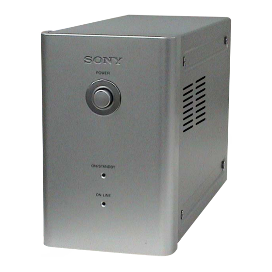
TA-FLX9W SECTION 1 This section is extracted from instruction manual. GENERAL 3 7 63 1515 0 LOCATION OF CONTROLS ALPHABETICAL ORDER A – Z ON LINE (indicator) 3 ON/STANDBY (indicator) 2 POWER 1 POWER ON/STANDBY ON LINE L 13942296513 u163 http://www.xiaoyu163.com... -
Page 4: Disassembly
TA-FLX9W SECTION 2 DISASSEMBLY 3 7 63 1515 0 • This set can be disassembled in the order shown below. 2-1. DISASSEMBLY FLOW 2-2. CASE (REAR AMPLIFIER) (Page 4) 2-3. VS BOARD (Page 5) 2-4. RX BOARD (Page 5) 2-5. -
Page 5: Vs Board
TA-FLX9W 3 7 63 1515 0 2-3. VS BOARD 2 two screws (BVTP 3 × 8) 4 insulation sheet 1 connector (CN972) 3 VS board (except Thai model) 1 connector (CN971) L 13942296513 2-4. RX BOARD 2 screw (BVTP 3 × 8) -
Page 6: Main Board
TA-FLX9W 3 7 63 1515 0 2-5. MAIN BOARD 1 connector (CN903) 2 screw (BVTP 3 × 8) 3 MAIN board 2 three screws (BVTP 3 × 8) L 13942296513 1 three connectors (CN102, CN104, CN105) u163 http://www.xiaoyu163.com... -
Page 7: Diagrams
TA-FLX9W SECTION 3 3 7 6 3 1 5 1 5 0 DIAGRAMS 3-1. BLOCK DIAGRAM TM101 IC7402 SPEAKERS RF DEMODULATOR, IMPEDANCE IC7407 IC7409 IF +5V A/D CONVERTER USE 8Ω D/A CONVERTER ELECTRICAL VOLUME J7401 IC101 10 ADVIN DAOUT... - Page 8 TA-FLX9W 3 7 6 3 1 5 1 5 0 • Note for Printed Wiring Boards and Schematic Diagrams • Circuit Board Location Note on Printed Wiring Boards: Note on Schematic Diagram: • X : parts extracted from the component side.
-
Page 9: Printed Wiring Board - Rx Board
TA-FLX9W • See page 8 for Circuit Boards Location. 3-2. PRINTED WIRING BOARD – RX Board – :Uses unleaded solder. 3 7 6 3 1 5 1 5 0 • Semiconductor RX BOARD (COMPONENT SIDE) Location Ref. No. Location... -
Page 10: Schematic Diagram - Rx Board (1/2)
TA-FLX9W 3 7 6 3 1 5 1 5 0 • See page 15 for IC Block Diagrams. • See page 8 for Waveform. 3-3. SCHEMATIC DIAGRAM – RX Board (1/2) – (1/2) Q7409,7410 B+ SWITCH C7414 C7428 C7442... -
Page 11: Schematic Diagram - Rx Board (2/2)
TA-FLX9W 3 7 6 3 1 5 1 5 0 • See page 8 for Waveform. • See page 17 for IC Pin Function Description. 3-4. SCHEMATIC DIAGRAM – RX Board (2/2) – (Page 10) (2/2) R7417 R7432 CN7403... -
Page 12: Printed Wiring Boards - Main Section
TA-FLX9W • See page 8 for Circuit Boards Location. 3-5. PRINTED WIRING BOARDS – MAIN Section – :Uses unleaded solder. 3 7 6 3 1 5 1 5 0 RX BOARD (Page 9) • Semiconductor CN7403 MAIN BOARD LED BOARD... -
Page 13: Printed Wiring Boards - Power Supply Section
TA-FLX9W • See page 8 for Circuit Boards Location. 3 7 6 3 1 5 1 5 0 3-6. PRINTED WIRING BOARDS – POWER SUPPLY Section – :Uses unleaded solder. • Semiconductor Location STBY BOARD VS BOARD (EXCEPT TH) Ref. -
Page 14: Schematic Diagram - Main Section
TA-FLX9W 3-7. SCHEMATIC DIAGRAM – MAIN Section – 3 7 6 3 1 5 1 5 0 L101 0.6µH POWER AMP IC101 LM3886T R125 R115 RY101 C113 0.047 R116 C153 0.047 REAR C175 0.047 C102 C106 C128 TM101 R108... - Page 15 TA-FLX9W 3 7 63 1515 0 • IC Block Diagrams – RX Board – IC7404 S-T111B15MC-OGATFG IC7401 TK11225CMCL-G VOUT ON/OFF OVER CURRENT PROTECTOR CONTROL CIRCUIT CONSTANT OVER HEAT & CURRENT OVER CURRENT SOURCE PROTECT ON/OFF REFERENCE CIRCUIT VOLTAGE CIRCUIT...
- Page 16 TA-FLX9W 3 7 63 1515 0 IC7407 PCM1751DBQR 15 14 ZERO DETECT SYSTEM FUNCTION CLOCK OUTPUT AMP AND CONTROL MANAGER CONVERTER LOW-PASS FILTER INTERFACE 8 TIME OVER SAMPLING ENHANCED DIGITAL FILTER MULTI-LEVEL WITH SYSTEM DELTA-SIGMA FUNCTION CLOCK MODULATOR CONTROLLER...
- Page 17 TA-FLX9W 3 7 63 1515 0 • IC Pin Function Description RX BOARD IC7405 MB89537APFM-G-598-BNDE1 (REAR AMP CONTROLLER) Pin No. Description Pin Name Not used MOD2 Setting terminal for the CPU operation mode Fixed at “L” in this set...
- Page 18 TA-FLX9W 3 7 63 1515 0 Pin No. Pin Name Description DIAT_SWDT Serial interface data write signal output to the RF demodulator DIAT_SRDT Serial interface data read signal input from the RF demodulator XSCEN Serial interface enable signal output to the RF demodulator —...
-
Page 19: Exploded Views
TA-FLX9W SECTION 4 EXPLODED VIEWS 3 7 63 1515 0 NOTE: • -XX and -X mean standardized parts, so they • Items marked “*” are not stocked since they The components identified by mark 0 or dotted line with mark 0 are may have some difference from the original are seldom required for routine service. -
Page 20: Chassis Section
TA-FLX9W 3 7 63 1515 0 4-2. CHASSIS SECTION F901 not supplied M101 not supplied (EXCEPT TH) not supplied not supplied not supplied (VS board) F971 not supplied L 13942296513 not supplied T901 The components identified by mark 0 or dotted line with mark 0 are critical for safety. -
Page 21: Electrical Parts List
TA-FLX9W SECTION 5 ELECTRICAL PARTS LIST 3 7 63 1515 0 MAIN NOTE: • Due to standardization, replacements in the • Items marked “*” are not stocked since they The components identified by mark 0 or dotted line with mark 0 are parts list may be different from the parts are seldom required for routine service. - Page 22 TA-FLX9W 3 7 63 1515 0 MAIN Ref. No. Part No. Description Remark Ref. No. Part No. Description Remark < FERRITE BEAD > R128 1-216-819-11 METAL CHIP 1/10W R129 1-216-817-11 METAL CHIP 1/10W FB101 1-469-152-11 FERRITE, EMI (SMD) (2012)
- Page 23 TA-FLX9W 3 7 63 1515 0 Ref. No. Part No. Description Remark Ref. No. Part No. Description Remark C7405 1-107-826-11 CERAMIC CHIP 0.1uF C7462 1-107-826-11 CERAMIC CHIP 0.1uF C7463 1-107-826-11 CERAMIC CHIP 0.1uF C7406 1-107-726-91 CERAMIC CHIP 0.01uF C7464...
- Page 24 TA-FLX9W 3 7 63 1515 0 STBY Ref. No. Part No. Description Remark Ref. No. Part No. Description Remark < RESISTOR > R7460 1-216-809-11 METAL CHIP 1/10W R7462 1-216-821-11 METAL CHIP 1/10W R7401 1-216-833-11 METAL CHIP 1/10W R7463 1-216-821-11 METAL CHIP...
- Page 25 TA-FLX9W 3 7 63 1515 0 STBY Ref. No. Part No. Description Remark Ref. No. Part No. Description Remark CN903 1-784-921-11 PIN, CONNECTOR 4P ACCESSORIES ************ < DIODE > 1-569-007-11 ADAPTOR, CONVERSION 2P (E15) D901 8-719-988-61 DIODE 1SS355TE-17 1-569-008-22 ADAPTOR, CONVERSION 2P (SP)
- Page 26 TA-FLX9W 3 7 63 1515 0 REVISION HISTORY Clicking the version allows you to jump to the revised page. Also, clicking the version at the upper right on the revised page allows you to jump to the next revised page.