Sign In
Upload
Manuals
Brands
Yamaha Manuals
Music Mixer
O1V 96
Yamaha O1V 96 Manuals
Manuals and User Guides for Yamaha O1V 96. We have
1
Yamaha O1V 96 manual available for free PDF download: Service Manual
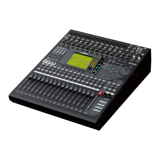
Yamaha O1V 96 Service Manual (228 pages)
DIGITAL MIXING CONSOLE
Brand:
Yamaha
| Category:
Music Mixer
| Size: 34.12 MB
Table of Contents
Table of Contents
1
Chemical Content Notice
2
Important Notice
2
Lithium Battery Handling
3
General Spec
4
Specifications (総合仕様
4
Digital Input
5
Option Input (SLOT)
5
EQ Parameters
7
Comp Parameters
8
Gate Parameters
8
Libraries
9
Analog Input Spec
10
Analog Output Spec
10
I/O Slot Spec
11
Digital Output Spec
11
Digital Input Spec
11
Control I/O Spec
12
Front View
12
Top View
12
Dimensions (寸法図
12
Control Panel
13
Panel Layout
13
AD Input Section
14
Monitor out & Headphones Section
14
Channel Strip Section
15
STEREO Section
15
DISPLAY ACCESS Section
16
FADER MODE Section
16
LAYER Section
16
ST in Section
16
SELECTED CHANNEL Section
17
Display Section
17
SCENE MEMORY Section
17
Data Entry Section
18
SOLO Section
18
USER DEFINED KEYS Section
18
AD Output Section
19
Phantom +48V
19
Rear Panel
19
SLOT Section
20
Digital I/O Section
20
Power Section
20
MIDI/Control Section
20
Bottom Assembly
21
Circuit Board Layout
21
Control Panel Assembly
22
Disassembly Procedure
23
Replacing the Lithium Battery
24
DCA Circuit Board
24
MAIN Circuit Board
24
Bottom Assembly Section
24
AC Circuit Board
26
AC Inlet Assembly
26
ADA Circuit Board
27
Control Panel Assembly Section
27
HA Circuit Board
27
FD Circuit Board
28
LCD Circuit Board and LCD
29
PN1 and PN1 Circuit Boards
30
PN2 Circuit Boards
30
Installing an Optional Card
32
オプションカードの取り付け
32
Lsi Pin Description (Lsi端子機能表
33
IC Block Diagram (ICブロック図
41
DCCOM (AC) Circuit Board
46
Circuit Boards (シート基板図
46
DCCOM Circuit Board
47
DCD Circuit Board (X3858B0)
48
FD Circuit Board (X3423B0)
50
HACOM (ADA) Circuit Board (X3422B0)
54
HACOM (ADA) Circuit Board
56
HACOM (HA) Circuit Board (X3422B0)
56
HACOM (HA) Circuit Board
58
MAIN Circuit Board (X3421B0)
62
PNCOM (PN1) Circuit Board
70
PNCOM (LCD) Circuit Board
75
Inspections
76
Preparations
76
Parameters
76
Initialization
76
Group Inspection
77
Recall Inspection
77
Analog In/Out Word Clock Int
77
Monitor out L/R
78
Odd Channel/Even Channel Crosstalk
78
Maximum Output
78
Gain
78
Distortion Ratio (both L/R)
79
Residual Noise (both L/R)
79
L/R Level Difference
79
Crosstalk between Left and Right
79
Gain Min
80
Distortion Ratio
80
Noise Level
80
Phones out L/R
81
2Tr Digital in
81
DIGITAL IN/OUT Inspection
81
WORD CLOCK Int96Khz
81
Jitter Measurement
82
Word Clock Int
82
Word Clock Ext
82
Service Check Program
90
Operation Method
90
Screen Explanation
90
List of Check Items
90
Service Check
91
Common Contents
91
PLLP2 Test
91
Service Check Connection Diagram
91
2TR IN/OUT (DIO) Test
92
Example of Execution Screen
92
ADAT Test
92
MIDI Test
92
PANEL LED Test
93
LCD Test
93
PANEL SW Test
93
Fader Move Test
93
ENCODER Test
94
Message Log
95
Supplement
95
Panel SW Operation Order Screen
95
SW Operation
96
LED Lighting Order
97
Audio Check
98
Outline
98
Check Method
98
Startup Method
98
Check Contents
99
Changing the Input/Output Terminals
99
Changing the Clock Source
99
Mode: Patch Setting During SLOT
100
Mode: Patch Setting During ADAT
101
Initializing the 01V96
114
01V96の初期化
114
Transmitting Parameter Settings Via MIDI (Bulk Dump)
115
CATEGORY Section
115
Request
115
内部設定をMIDI経由で出力(バルクダンプ機能
117
Calibrating the Faders
119
Checking the Battery and the System Version (バッテリーの残量やシステムのバージョンの確認
119
フェーダーのキャリブレーション
119
MIDI Data Format
120
Data Format
120
Channel Message
120
Format Details
120
System Common Message
120
Control Change
120
Program Change
121
Timing Clock
121
System Exclusive Message
121
Bulk Dump
121
Scene Memory Bulk Dump Request Format
122
Setup Memory Bulk Dump Request Format
122
User Defined MIDI Remote Bulk Dump Format
122
Setup Memory Bulk Dump Format
122
User Defined Keys Bulk Dump Format
123
User Assignable Layer Bulk Dump Request Format
123
User Defined Keys Bulk Dump Request Format
123
Control Change Table Bulk Dump Format
123
Program Change Table Bulk Dump Format
124
Program Change Table Bulk Dump Request Format
124
Equalizer Library Bulk Dump Request Format
124
Compressor Library Bulk Dump Format
124
Compressor Library Bulk Dump Request Format
125
Gate Library Bulk Dump Format
125
Effect Library Bulk Dump Format
125
Effect Library Bulk Dump Request Format
125
Channel Library Bulk Dump Request Format
126
Input Patch Library Bulk Dump Request Format
126
Output Patch Library Bulk Dump Format
126
Output Patch Library Bulk Dump Request Format
126
Plug-In Effect Card Bulk Dump Format
127
Parameter Change Basic Format
127
Plug-In Effect Card Bulk Dump Request Format
127
Parameter Change
127
Parameter Request (Function Call: Attribute)
131
Parameter Change (Function Call Response: Link)
131
Parameter Change (Function Call: Pair , Copy)
131
Parameter Change (Function Call Event: Effect )
132
Parameter Change (Remote Time Counter)
133
Parameter Request (Remote Time Counter)
133
MIDI Implementation Chart
134
Parts List
135
Overall Assembly
136
Top View
139
Circuit Diagram
190
Block Diagram 002 (01V96)
191
Block Diagram 003 (01V96)
192
Block Diagram 005 (01V96)
194
Block Diagram 006 (01V96)
195
Overall Connector Circuit Diagram (01V96)
196
Ac Circuit Diagram (01V96)
197
Dca Circuit Diagram (01V96)
198
DCD Circuit Diagram (01V96)
199
Fd Circuit Diagram 002 (01V96)
200
Fd Circuit Diagram 003 (01V96)
201
Fd Circuit Diagram 004 (01V96)
202
Fd Circuit Diagram 005 (01V96)
203
Fd Circuit Diagram 006 (01V96)
204
Ada Circuit Diagram 002 (01V96)
205
Ada Circuit Diagram 003 (01V96)
206
Ada Circuit Diagram 004 (01V96)
207
Ha Circuit Diagram 002 (01V96)
208
Ha Circuit Diagram 003 (01V96)
209
Ha Circuit Diagram 004 (01V96)
210
Main Circuit Diagram 002 (01V96)
211
Main Circuit Diagram 003 (01V96)
212
Main Circuit Diagram 004 (01V96)
213
Main Circuit Diagram 005 (01V96)
214
Main Circuit Diagram 006 (01V96)
215
Main Circuit Diagram 007 (01V96)
216
Main Circuit Diagram 008 (01V96)
217
Main Circuit Diagram 009 (01V96)
218
Main Circuit Diagram 010 (01V96)
219
Main Circuit Diagram 011 (01V96)
220
Main Circuit Diagram 012 (01V96)
221
Main Circuit Diagram 013 (01V96)
222
Lcd Circuit Diagram (01V96)
223
Pn1 Circuit Diagram 002 (01V96)
224
Pn1 Circuit Diagram 003 (01V96)
225
Pn1 Circuit Diagram 004 (01V96)
226
Pn2 Circuit Diagram (01V96)
227
Advertisement
Advertisement
Related Products
Yamaha OIV96i
Yamaha O3D
Yamaha O2R 96 version 2
Yamaha O1V96
Yamaha O1v
Yamaha O2R96
Yamaha O1V96i
Yamaha Operations
Yamaha Oak Custom
Yamaha O2R v2
Yamaha Categories
Motorcycle
Musical Instrument
Electronic Keyboard
Receiver
Amplifier
More Yamaha Manuals
Login
Sign In
OR
Sign in with Facebook
Sign in with Google
Upload manual
Upload from disk
Upload from URL