Sign In
Upload
Manuals
Brands
MOTOROLA Manuals
Portable Radio
MTX series
MOTOROLA MTX series Manuals
Manuals and User Guides for MOTOROLA MTX series. We have
7
MOTOROLA MTX series manuals available for free PDF download: Detailed Service Manual, Programmer's Reference Manual, Service Manual, Theory/Troubleshooting Manual
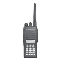
Motorola MTX series Detailed Service Manual (639 pages)
Detailed service manual for Two-Way Radios
Brand:
Motorola
| Category:
Two-Way Radio
| Size: 31.13 MB
Table of Contents
Computer Software Copyrights
2
Disclaimer
2
Document Copyrights
2
Foreword
2
Product Safety and Rf Exposure Compliance
2
Trademarks
2
Document History
3
Table of Contents
5
List of Figures
9
Related Publications
19
FMRC Approved Equipment
21
Intrinsically Safe Radio Information
21
Repair of FMRC Approved Products
22
Do Not Substitute Options or Accessories
23
Chapter 1 Introduction
25
Scope of Manual
25
Warranty and Service Support
25
Piece Parts
26
Technical Support
26
Further Assistance from Motorola
26
Radio Model Chart and Specification
27
Radio Model Information
27
Chapter 2 Radio Power Distribution
29
Figure 2-1. DC Power Distribution Block Diagram
29
Chapter 3 Keypad
31
Figure 3-1. Keypad Block Diagram
31
Controller Board
32
Figure 3-2. Controller Block Diagram
32
Figure 3-3. RTC Circuit
33
Chapter 4 UHF Band 1 Theory of Operation
35
Transmitter
35
Figure 4-1. Transmitter Block Diagram
35
Antenna Matching Network
36
Antenna Switch
36
Harmonic Filter
36
Receiver
37
Figure 4-2. UHF Receiver Block Diagram
37
Frequency Generation Circuitry
38
Figure 4-3. Frequency Generation Unit Block Diagram
38
Synthesizer
39
Figure 4-4. Synthesizer Block Diagram
39
Voltage-Controlled Oscillator (VCO)
40
Figure 4-5. VCO Block Diagram
40
Chapter 5 UHF Band 2 Theory of Operation
43
Transmitter
43
Figure 5-1. Transmitter Block Diagram
43
Receiver
45
Figure 5-2. UHF Receiver Block Diagram
45
Frequency Generation Circuitry
46
Figure 5-3. Frequency Generation Unit Block Diagram
46
Synthesizer
47
Figure 5-4. Synthesizer Block Diagram
47
Voltage-Controlled Oscillator (VCO)
48
Figure 5-5. VCO Block Diagram
48
Chapter 6 VHF Theory of Operation
51
Transmitter
51
Figure 6-1. Transmitter Block Diagram
51
Receiver (for All Models Except those with PCB 8486473Z04)
53
Figure 6-2. VHF Receiver Block Diagram
53
Receiver (for Models with PCB 8486473Z04)
55
Figure 6-3. VHF Receiver Block Diagram
55
Frequency Generation Circuitry
58
Figure 6-4. Frequency Generation Unit Block Diagram
58
Synthesizer
59
Figure 6-5. Synthesizer Block Diagram
59
Voltage-Controlled Oscillator (VCO)
60
Figure 6-6. VCO Block Diagram
60
Chapter 7 Low Band, 800 Mhz, Passport & 900 Mhz Theory of Operation
63
Introduction
63
Low Band Transmitter
63
Figure 7-1. Low Band Transmitter Block Diagram
63
Low Band Receiver
65
Figure 7-2. Low Band Receiver Block Diagram
65
Synthesizer
67
Figure 7-3. Low Band Frequency Generation Unit Block Diagram
67
Voltage Control Oscillators (VCO)
68
Figure 7-4. Low Band Synthesizer Block Diagram
68
800 Mhz Transmitter
69
Figure 7-5. 800 Mhz Transmitter Block Diagram
69
800 Mhz Receiver
71
Synthesizer
74
Figure 7-8. 800 Mhz Frequency Generation Unit Block Diagram
74
Figure 7-9. 800 Mhz Synthesizer Block Diagram
75
Figure 7-10. 800 Mhz VCO Block Diagram
76
Trunked Radio Systems
77
Power Supplies
78
7.10 900 Mhz Transmitter
79
Figure 7-11. Transmitter Block Diagram
79
Power Amplifier
80
7.11 900 Mhz Receiver
81
Figure 7-12. 900 Mhz Receiver Block Diagram (for PCB No. 8485910Z01)
81
Figure 7-13. 900 Mhz Receiver Block Diagram (for PCB No. 8471203M01)
82
7.12 Frequency Generation Circuitry
86
7.13 900 Mhz Synthesizer
86
Figure 7-14. Frequency Generation Unit Block Diagram
86
Figure 7-15. Synthesizer Block Diagram
87
900 Mhz Voltage Control Oscillator (VCO)
88
Figure 7-16. VCO Block Diagram
88
Chapter 8 Maintenance
91
Introduction
91
Preventive Maintenance
91
Inspection
91
Safe Handling of CMOS and LDMOS
92
General Repair Procedures and Techniques
92
Recommended Test Tools
94
Replacing the Circuit Board Fuse
95
Figure 8-1. Uhf/Vhf/Low Band/800 Mhz/900 Mhz Circuit Board Fuse Locations
95
Removing and Reinstalling the Circuit Board
96
Figure 8-2. Circuit Board Removal and Reinstallation
96
Power up Self-Test Error Codes
97
8.10 UHF Band 1 Troubleshooting Charts
98
Troubleshooting Flow Chart for Transmitter
104
Troubleshooting Flow Chart for Synthesizer
105
Troubleshooting Flow Chart for Vco
106
8.11 UHF Band 2 Troubleshooting Charts
107
8.12 VHF Troubleshooting Charts
116
8.13 Low Band Troubleshooting Charts
125
8.14 800 Mhz Troubleshooting Charts
131
8.15 Passport Trunking Troubleshooting Chart
140
8.16 Keypad Troubleshooting Chart
141
8.17 900 Mhz Troubleshooting Charts
142
Chapter 9 Schematic Diagrams, Overlays, and Parts Lists
151
Introduction
151
Flex Layout
152
Figure 9-1. Keypad-Controller Interconnect Flex
153
Figure 9-2. Keypad-Controller Interconnect Flex Schematic Diagram
153
Figure 9-3. Universal Flex Connector
154
Figure 9-4. Universal Flex Connector Schematic Diagram
155
Keypad Top and Bottom Overlays
156
Figure 9-5. Keypad Top and Bottom Board Overlays
156
Keypad Circuit Board/Schematic Diagrams and Parts List
157
Figure 9-6. Keypad Board (5000 and 7000 Series) Schematic Diagram
157
Figure 9-7. 9000 Series Keypad Top and Bottom Board Overlays
159
Figure 9-8. 9000 Series Keypad Board Schematic Diagram
160
Controller Circuit Board/Schematic Diagrams and Parts List
163
Figure 9-9. VHF/UHF Complete Controller Schematic Diagram
163
Figure 9-10. VHF/UHF Controller ASFIC/ON_OFF Schematic Diagram
164
Figure 9-11. VHF/UHF Controller ASFIC/ON_OFF Schematic Diagram
165
Figure 9-12. VHF/UHF Controller Microprocessor Schematic Diagram
166
Figure 9-13. VHF/UHF Controller Microprocessor Schematic Diagram
167
Figure 9-14. Controller Memory Schematic Diagram
168
Figure 9-15. Controller Audio Power Amplifier Schematic Diagram
169
Figure 9-16. Controller Interface Schematic Diagram
170
UHF Band 1 Circuit Board/Schematic Diagrams and Parts List (PCB 8480450Z03)
171
Figure 9-17. UHF (403-470 Mhz) 5000/7000 Series Main Board Top Side
171
Figure 9-18. UHF (403-470 Mhz) 5000/7000 Series Main Board Bottom Side
172
Figure 9-19. UHF (403-470 Mhz) Controls and Switches Schematic Diagram
173
Figure 9-20. UHF (403-470 Mhz) Receiver Front End Schematic Diagram
174
Figure 9-21. UHF (403-470 Mhz) Receiver Back End Schematic Diagram
175
Figure 9-22. UHF (403-470 Mhz) Synthesizer Schematic Diagram
176
Figure 9-23. UHF (403-470 Mhz) Voltage Controlled Oscillator Schematic Diagram
177
Figure 9-24. UHF (403-470 Mhz) Transmitter Schematic Diagram
178
UHF Band 1 Circuit Board/Schematic Diagrams and Parts List (PCB 8480450Z13 / 8480587Z05)
183
Figure 9-25. UHF (403-470 Mhz) 5000/7000 Series Main Board Top Side
183
Figure 9-26. UHF (403-470 Mhz) 5000/7000 Series Main Board Bottom Side
184
Figure 9-27. UHF (403-470 Mhz) 5000/7000 Series Main Board Top Side
185
Figure 9-28. UHF (403-470 Mhz) 5000/7000 Series Main Board Bottom Side
186
Figure 9-29. UHF (403-470 Mhz) Controls and Switches Schematic Diagram
187
Figure 9-30. UHF (403-470 Mhz) Receiver Front End Schematic Diagram
188
Figure 9-31. UHF (403-470 Mhz) Receiver Back End Schematic Diagram
189
Figure 9-32. UHF (403-470 Mhz) Synthesizer Schematic Diagram
190
Figure 9-33. UHF (403-470 Mhz) Voltage Controlled Oscillator Schematic Diagram
191
Figure 9-34. UHF (403-470 Mhz) Transmitter Schematic Diagram
192
UHF Band 1 Circuit Board/Schematic Diagrams and Parts List (PCB 8480450Z14)
197
Figure 9-35. UHF (403-470 Mhz) 5000/7000 Series Main Board Top Side PCB No. 8480450Z14
197
Figure 9-36. UHF (403-470 Mhz) 5000/7000 Series Main Board Bottom Side PCB No. 8480450Z14
198
Figure 9-37. UHF (403-470 Mhz) Controls and Switches Schematic Diagram
199
Figure 9-38. UHF (403-470 Mhz) Receiver Front End Schematic Diagram
200
Figure 9-39. UHF (403-470 Mhz) Receiver Back End Schematic Diagram
201
Figure 9-40. UHF (403-470 Mhz) Synthesizer Schematic Diagram
202
Figure 9-41. UHF (403-470 Mhz) Voltage Controlled Oscillator Schematic Diagram
203
Figure 9-42. UHF (403-470 Mhz) Harmonic Filter Schematic Diagram
204
Figure 9-43. UHF (403-470 Mhz) Transmitter Schematic Diagram
205
Figure 9-44. UHF (403-470 Mhz) Complete Controller Schematic Diagram
206
Figure 9-45. UHF (403-470 Mhz) Controller ASFIC/ON_OFF Schematic Diagram
207
Figure 9-46. UHF (403-470 Mhz) Controller Microprocessor Schematic Diagram
208
Figure 9-47. UHF (403-430 Mhz) Controller Memory Schematic Diagram
209
Figure 9-48. UHF (403-470 Mhz) Controller Audio Power Amplifier Schematic
210
Figure 9-49. UHF (403-470 Mhz) Controller Interface Schematic Diagram
211
UHF Band 1 Circuit Board/Schematic Diagrams and Parts List (PCB 8486458Z02)
217
Figure 9-50. UHF (403-470 Mhz) 5000/7000 Series Main Board Top Side PCB No. 8486458Z02
217
Figure 9-51. UHF (403-470 Mhz) 5000/7000 Series Main Board Bottom Side PCB No. 8486458Z02
218
Figure 9-52. UHF (403-470 Mhz) Controls and Switches Schematic Diagram
219
Figure 9-53. UHF (403-470 Mhz) Receiver Front-End Schematic Diagram
220
Figure 9-54. UHF (403-470 Mhz) Receiver Back-End Schematic Diagram
221
Figure 9-55. UHF (403-470 Mhz) Synthesizer Schematic Diagram
222
Figure 9-56. UHF (403-470 Mhz) Voltage Controlled Oscillator Schematic Diagram
223
Figure 9-57. UHF (403-470 Mhz) Harmonic Filter Schematic Diagram
224
Figure 9-58. UHF (403-470 Mhz) Transmitter Schematic Diagram
225
Figure 9-59. UHF (403-470 Mhz) Controller ASFIC/ON_OFF Schematic Diagram
226
UHF Band 1 Circuit Board/Schematic Diagrams and Parts List (PCB 8486458Z03)
231
Figure 9-60. UHF (403-470 Mhz) 5000/7000 Series Main Board Top Side PCB No. 8486458Z03
231
Figure 9-61. UHF (403-470 Mhz) 5000/7000 Series Main Board Bottom Side PCB No. 8486458Z03
232
Figure 9-62. UHF (403-470 Mhz) Controls and Switches Schematic Diagram
233
Figure 9-63. UHF (403-470 Mhz) Receiver Front End Schematic Diagram
234
Figure 9-64. UHF (403-470 Mhz) Receiver Back End Schematic Diagram
235
Figure 9-65. UHF (403-470 Mhz) Synthesizer Schematic Diagram
236
Figure 9-66. UHF (403-470 Mhz) Voltage Controlled Oscillator Schematic Diagram
237
Figure 9-67. UHF (403-470 Mhz) Harmonic Filter Schematic Diagram
238
Figure 9-68. UHF (403-470 Mhz) Transmitter Schematic Diagram
239
Figure 9-69. UHF (403-470 Mhz) Complete Controller Schematic Diagram
240
Figure 9-70. UHF (403-470 Mhz) Controller ASFIC/ON_OFF Schematic Diagram
241
Figure 9-71. UHF (403-470 Mhz) Controller Microprocessor Schematic Diagram
242
Figure 9-72. UHF (403-430 Mhz) Controller Memory Schematic Diagram
243
Figure 9-73. UHF (403-470 Mhz) Controller Audio Power Amplifier Schematic
244
Figure 9-74. UHF (403-470 Mhz) Controller Interface Schematic Diagram
245
UHF Band 1 Circuit Board/Schematic Diagrams and Parts List (PCB 8415234H01, 8415234H02, 8415234H05, 8415234H08)
251
Figure 9-75. UHF (403-470 Mhz) Main Board Top Side PCB No. 8415234H01
251
Figure 9-76. UHF (403-470 Mhz) Main Board Bottom Side PCB No. 8415234H01
252
Figure 9-77. UHF (403-470 Mhz) Main Board Top Side PCB No. 8415234H02
253
Figure 9-78. UHF (403-470 Mhz) Main Board Bottom Side PCB No. 8415234H02
254
Figure 9-79. UHF (403-470 Mhz) Main Board Top Side PCB No. 8415234H05
255
Figure 9-80. UHF (403-470 Mhz) Main Board Bottom Side PCB No. 8415234H05
256
Figure 9-81. UHF (403-470 Mhz) Main Board Top Side PCB No. 8415234H08
257
Figure 9-82. UHF (403-470 Mhz) Main Board Bottom Side PCB No. 8415234H08
258
Figure 9-83. UHF Controls and Switches Schematic Diagram for (403-470Mhz for 8415234H01)
259
Figure 9-84. UHF Controls and Switches Schematic Diagram for
260
Figure 9-85. UHF Controls and Switches Schematic Diagram for
261
Figure 9-86. UHF Controls and Switches Schematic Diagram for (403-470Mhz for 8415234H08)
262
Figure 9-87. UHF Receiver Front End Schematic Diagram for
263
Figure 9-88. UHF Receiver Front End Schematic Diagram for
264
Figure 9-89. UHF Receiver Front End Schematic Diagram for
265
Figure 9-90. UHF Receiver Front End Schematic Diagram for
266
Figure 9-91. UHF Receiver Back End Schematic Diagram for (403-470Mhz for 8415234H01)
267
Figure 9-92. UHF Receiver Back End Schematic Diagram for
268
Figure 9-93. UHF Receiver Back End Schematic Diagram for (403-470Mhz for 8415234H05)
269
Figure 9-94. UHF Receiver Back End Schematic Diagram for (403-470Mhz for 8415234H08)
270
Figure 9-95. UHF Synthesizer Schematic Diagram
271
Figure 9-96. UHF Voltage Controlled Oscillator Schematic Diagram
272
Figure 9-97. UHF Harmonic Filter Schematic Diagram for
273
Figure 9-98. UHF Harmonic Filter Schematic Diagram for
274
Figure 9-99. UHF Harmonic Filter Schematic Diagram for
275
Figure 9-100.UHF Harmonic Filter Schematic Diagram for
276
Figure 9-101.UHF Transmitter Schematic Diagram for
277
Figure 9-102.UHF Transmitter Schematic Diagram for
278
Figure 9-103.UHF Transmitter Schematic Diagram for
279
Figure 9-104.UHF Transmitter Schematic Diagram for
280
Figure 9-105.Complete Controller Schematic Diagram for (403-470Mhz for 8415234H01, 8415234H05, 8415234H08)
281
Figure 9-106.Controller ASFIC/ON_OFF Schematic Diagram for (403-470Mhz for 8415234H01, 8415234H05, 8415234H08)
282
Figure 9-107.Controller Microprocessor Schematic Diagram for (403-470Mhz for 8415234H01, 8415234H05, 8415234H08)
283
Figure 9-108.Controller Memory Schematic Diagram for (403-470Mhz for 8415234H01, 8415234H05, 8415234H08)
284
Figure 9-109.Controller Audio Power Amplifier Schematic Diagram for
285
Figure 9-110.Controller Interface Schematic Diagram for (403-470Mhz for 8415234H01, 8415234H05, 8415234H08)
286
9.12 UHF Band 1 Circuit Board/Schematic Diagrams and Parts List
313
Figure 9-90. UHF (403-470 Mhz) 9000 Series Main Board Top Side PCB
313
Figure 9-91. UHF (403-470 Mhz) 9000 Series Main Board Bottom Side PCB
314
Figure 9-92. UHF (403-470 Mhz) Controls and Switches Schematic Diagram
315
Figure 9-93. UHF (403-470 Mhz) Receiver Front End Schematic Diagram
316
Figure 9-94. UHF (403-470 Mhz) Receiver Back End Schematic Diagram
317
Figure 9-95. UHF (403-470 Mhz) Synthesizer Schematic Diagram
318
Figure 9-96. UHF (403-470 Mhz) Voltage Controlled Oscillator Schematic Diagram
319
Figure 9-97. UHF (403-470 Mhz) Transmitter Schematic Diagram
320
UHF Band 2 Circuit Board/Schematic Diagrams and Parts List (PCB 8485641Z02)9-175
325
Figure 9-98. UHF (450-527 Mhz) 5000/7000 Series Main Board Top Side
325
Figure 9-99. UHF (450-527 Mhz) 5000/7000 Series Main Board Bottom Side
326
Figure 9-100.UHF (450-527 Mhz) Controls and Switches Schematic Diagram
327
Figure 9-101.UHF (450-527 Mhz) Receiver Front End Schematic Diagram
328
Figure 9-102.UHF (450-527 Mhz) Receiver Back End Schematic Diagram
329
Figure 9-103.UHF (450-527 Mhz) Synthesizer Schematic Diagram
330
Figure 9-104.UHF (450-527 Mhz) Voltage Controlled Oscillator Schematic Diagram
331
Figure 9-105.UHF (450-527 Mhz) Transmitter Schematic Diagram
332
UHF Band 2 Circuit Board/Schematic Diagrams and Parts List (PCB 8485641Z06 / 8485677Z03)
337
Figure 9-106.UHF (450-527 Mhz) 5000/7000 Series Main Board Top Side
337
Figure 9-107.UHF (450-527 Mhz) 5000/7000 Series Main Board Bottom Side
338
Figure 9-108.UHF (450-527 Mhz) 5000/7000 Series Main Board Top Side
339
Figure 9-109.UHF (450-527 Mhz) 5000/7000 Series Main Board Bottom Side
340
Figure 9-110.UHF (450-527 Mhz) Controls and Switches Schematic Diagram
341
Figure 9-111.UHF (450-527 Mhz) Receiver Front End Schematic Diagram
342
Figure 9-112.UHF (450-527 Mhz) Receiver Back End Schematic Diagram
343
Figure 9-113.UHF (450-527 Mhz) Synthesizer Schematic Diagram
344
Figure 9-114.UHF (450-527 Mhz) Voltage Controlled Oscillator Schematic Diagram
345
Figure 9-115.UHF (450-527 Mhz) Transmitter Schematic Diagram
346
Figure 9-116.UHF (450-527 Mhz) 5000/7000 Series Main Board Top Side
351
Figure 9-117.UHF (450-527 Mhz) 5000/7000 Series Main Board Bottom Side PCB No. 8486686Z01
352
Figure 9-118.UHF (450-527 Mhz) Controls and Switches Schematic Diagram
353
Figure 9-119.UHF (450-527 Mhz) Receiver Front End Schematic Diagram
354
Figure 9-120.UHF (450-527 Mhz) Receiver Back End Schematic Diagram
355
Figure 9-121.UHF (450-527 Mhz) Synthesizer Schematic Diagram
356
Figure 9-122.UHF (450-527 Mhz) Voltage Controlled Oscillator Schematic Diagram
357
Figure 9-123.UHF (450-527 Mhz) Harmonic Filter Schematic Diagram
358
Figure 9-124.UHF (450-527 Mhz) Transmitter Schematic Diagram
359
Figure 9-125.UHF (450-527 Mhz) Controller ASFIC/ON_OFF Schematic Diagram
360
Figure 9-126.UHF (450-527 Mhz) 5000/7000 Series Main Board Top Side
365
Figure 9-127.UHF (450-527 Mhz) 5000/7000 Series Main Board Bottom Side PCB No. 8486686Z02
366
Figure 9-128.UHF (450-527 Mhz) Controls and Switches Schematic Diagram
367
Figure 9-129.UHF (450-527 Mhz) Receiver Front End Schematic Diagram
368
Figure 9-130.UHF (450-527 Mhz) Receiver Back End Schematic Diagram
369
Figure 9-131.UHF (450-527 Mhz) Synthesizer Schematic Diagram
370
Figure 9-132.UHF (450-527 Mhz) Voltage Controlled Oscillator Schematic Diagram
371
Figure 9-133.UHF (450-527 Mhz) Harmonic Filter Schematic Diagram
372
Figure 9-134.UHF (450-527 Mhz) Transmitter Schematic Diagram
373
Figure 9-135.UHF (450-527 Mhz) Complete Controller Schematic Diagram
374
Figure 9-136.UHF (450-527 Mhz) Controller ASFIC/ON_OFF Schematic Diagram
375
Figure 9-137.UHF (450-527 Mhz) Controller Microprocessor Schematic Diagram
376
Figure 9-138.UHF (450-527 Mhz) Controller Memory Schematic Diagram
377
Figure 9-139.UHF (450-527 Mhz) Controller Audio Power Amplifier Schematic
378
Figure 9-140.UHF (450-527 Mhz) Controller Interface Schematic Diagram
379
UHF Band 2 Circuit Board/Schematic Diagrams and Parts List (PCB 8486686Z02)9-215
381
UHF Band 2 Circuit Board/Schematic Diagrams and Parts List (PCB 8415235H01, 8415235H05)
385
Figure 9-141.UHF Band 2 (450-527 Mhz) Main Board Top Side
385
Figure 9-142.UHF Band 2 (450-527 Mhz) Main Board Bottom Side
386
Figure 9-143.UHF Band 2 (450-527 Mhz) Main Board Top Side
387
Figure 9-144.UHF Band 2 (450-527 Mhz) Main Board Bottom Side
388
Figure 9-145.UHF Band 2 Controls and Switches Schematic Diagram
389
Figure 9-146.UHF Band 2 Controls and Switches Schematic Diagram
390
Figure 9-147.UHF Band 2 Receiver Front End Schematic Diagram
391
Figure 9-148.UHF Band 2 Receiver Front End Schematic Diagram
392
Figure 9-149.UHF Band 2 Receiver Back End Schematic Diagram
393
Figure 9-150.UHF Band 2 Receiver Back End Schematic Diagram
394
Figure 9-151.UHF Band 2 Synthesizer Schematic Diagram
395
Figure 9-152.UHF Band 2 Voltage Controlled Oscillator Schematic Diagram
396
Figure 9-153.UHF Band 2 Harmonic Filter Schematic Diagram
397
Figure 9-154.UHF Band 2 Harmonic Filter Schematic Diagram
398
Figure 9-155.UHF Band 2 Transmitter Schematic Diagram
399
Figure 9-156.UHF Band 2 Transmitter Schematic Diagram
400
Figure 9-157.Complete Controller Schematic Diagram
401
Figure 9-158.Controller ASFIC/ON_OFF Schematic Diagram
402
Figure 9-159.Controller Microprocessor Schematic Diagram
403
Figure 9-160.Controller Memory Schematic Diagram
404
Figure 9-161.Controller Audio Power Amplifier Schematic Diagram
405
Figure 9-162.Controller Interface Schematic Diagram
406
9.18 UHF Band 2 Circuit Board/Schematic Diagrams and Parts List
421
Figure 9-156.UHF (450-527 Mhz) 9000 Series Main Board Top Side PCB
421
Figure 9-157.UHF (450-527 Mhz) 9000 Series Main Board Bottom Side PCB
422
Figure 9-158.UHF (450-527 Mhz) Controls and Switches Schematic Diagram
423
Figure 9-159.UHF (450-527 Mhz) Receiver Front End Schematic Diagram
424
Figure 9-160.UHF (450-527 Mhz) Receiver Back End Schematic Diagram
425
Figure 9-161.UHF (450-527 Mhz) Synthesizer Schematic Diagram
426
Figure 9-162.UHF (450-527 Mhz) Voltage Controlled Oscillator Schematic Diagram
427
Figure 9-163.UHF (450-527 Mhz) Transmitter Schematic Diagram
428
Figure 9-164.UHF (450-527 Mhz) Voice Storage Schematic Diagram
429
VHF Circuit Board/Schematic Diagrams and Parts List (PCB 8486062B09)
433
Figure 9-165.VHF (136-174 Mhz) 5000/7000 Series Main Board Top Side
433
Figure 9-166.VHF (136-174 Mhz) 5000/7000 Series Main Board Bottom Side
434
Figure 9-167.VHF (136-174 Mhz) Controls and Switches Schematic Diagram
435
Figure 9-168.VHF (136-174 Mhz) Receiver Front End Schematic Diagram
436
Figure 9-169.VHF (136-174 Mhz) Receiver Back End Schematic Diagram
437
Figure 9-170.VHF (136-174 Mhz) Synthesizer Schematic Diagram
438
Figure 9-171.VHF (136-174 Mhz) Voltage Controlled Oscillator Schematic Diagram
439
Figure 9-172.VHF (136-174 Mhz) Transmitter Schematic Diagram
440
VHF Circuit Board/Schematic Diagrams and Parts List (PCB 8486062B12)
445
Figure 9-173.VHF (136-174 Mhz) 5000/7000 Series Main Board Top Side
445
Figure 9-174.VHF (136-174 Mhz) 5000/7000 Series Main Board Bottom Side
446
Figure 9-175.VHF (136-174 Mhz) Controls and Switches Schematic Diagram
447
Figure 9-176.VHF (136-174 Mhz) Receiver Front End Schematic Diagram
448
Figure 9-177.VHF (136-174 Mhz) Receiver Back End Schematic Diagram
449
Figure 9-178.VHF (136-174 Mhz) Synthesizer Schematic Diagram
450
Figure 9-179.VHF (136-174 Mhz) Voltage Controlled Oscillator Schematic Diagram
451
Figure 9-180.VHF (136-174 Mhz) Transmitter Schematic Diagram
452
VHF Circuit Board/Schematic Diagrams and Parts List (PCB 8486062B16 / 8486062B17 / 8486101B11)
457
Figure 9-181.VHF (136-174 Mhz) 5000/7000 Series Main Board Top Side
457
Figure 9-182.VHF (136-174 Mhz) 5000/7000 Series Main Board Bottom Side
458
Figure 9-183.VHF (136-174 Mhz) 5000/7000 Series Main Board Top Side
459
Figure 9-184.VHF (136-174 Mhz) 5000/7000 Series Main Board Bottom Side
460
Figure 9-185.VHF (136-174 Mhz) 5000/7000 Series Main Board Top Side
461
Figure 9-186.VHF (136-174 Mhz) 5000/7000 Series Main Board Bottom Side
462
Figure 9-187.VHF (136-174 Mhz) Controls and Switches Schematic Diagram
463
Figure 9-188.VHF (136-174 Mhz) Receiver Front End Schematic Diagram
464
Figure 9-189.VHF (136-174 Mhz) Receiver Back End Schematic Diagram
465
Figure 9-190.VHF (136-174 Mhz) Synthesizer Schematic Diagram
466
Figure 9-191.VHF (136-174 Mhz) Voltage Controlled Oscillator Schematic Diagram
467
Figure 9-192.VHF (136-174 Mhz) Transmitter Schematic Diagram
468
VHF Circuit Board/Schematic Diagrams and Parts List (PCB 8486473Z03)
473
Figure 9-193.VHF (136-174 Mhz) 5000/7000 Series Main Board Top Side PCB No. 8486473Z03
473
Figure 9-194.VHF (136-174 Mhz) 5000/7000 Series Main Board Bottom Side PCB No. 8486473Z03
474
Figure 9-195.VHF (136-174 Mhz) Controls and Switches Schematic Diagram
475
Figure 9-196.VHF (136-174 Mhz) Receiver Front-End Schematic Diagram
476
Figure 9-197.VHF (136-174 Mhz) Receiver Back-End Schematic Diagram
477
Figure 9-198.VHF (136-174 Mhz) Synthesizer Schematic Diagram
478
Figure 9-199.VHF (136-174 Mhz) Voltage Controlled Oscillator Schematic Diagram
479
Figure 9-200.VHF (136-174 Mhz) Transmitter Schematic Diagram
480
Figure 9-201.VHF (136-174 Mhz) Controller ASFIC/ON_OFF Schematic Diagram
481
VHF Circuit Board/Schematic Diagrams and Parts List (PCB 8486473Z04)
487
Figure 9-202.VHF (136-174 Mhz) 5000/7000 Series Main Board Top Side PCB No. 8486473Z04
487
Figure 9-203.VHF (136-174 Mhz) 5000/7000 Series Main Board Bottom Side PCB No. 8486473Z04
488
Figure 9-204.VHF (136-174 Mhz) Controls and Switches Schematic Diagram
489
Figure 9-205.VHF (136-174 Mhz) Receiver Front End Schematic Diagram
490
Figure 9-206.VHF (136-174 Mhz) Receiver Back End Schematic Diagram
491
Figure 9-207.VHF (136-174 Mhz) Synthesizer Schematic Diagram
492
Figure 9-208.VHF (136-174 Mhz) Voltage Controlled Oscillator Schematic Diagram
493
Figure 9-209.VHF (136-174 Mhz) Transmitter Schematic Diagram
494
Figure 9-210.VHF (136-174 Mhz) Complete Controller Schematic Diagram
495
Figure 9-211.VHF (136-174 Mhz) Controller ASFIC/ON_OFF Schematic Diagram
496
Figure 9-212.VHF (136-174 Mhz) Controller Microprocessor Schematic Diagram
497
Figure 9-213.VHF (136-174 Mhz) Controller Memory Schematic Diagram
498
Figure 9-214.VHF (136-174 Mhz) Controller Audio Power Amplifier
499
Figure 9-215.VHF (136-174 Mhz) Controller Interface Schematic Diagram
500
VHF Circuit Board/Schematic Diagrams and Parts List (PCB 8415112H01)
507
Figure 9-216.VHF (136-174 Mhz) Main Board Top Side
507
Figure 9-217.VHF (136-174 Mhz) Main Board Bottom Side
508
Figure 9-218.VHF Controls and Switches Schematic Diagram
509
Figure 9-219.VHF Receiver Front End Schematic Diagram
510
Figure 9-220.VHF Receiver Back End Schematic Diagram
511
Figure 9-221.VHF Synthesizer Schematic Diagram
512
Figure 9-222.VHF Voltage Controlled Oscillator Schematic Diagram
513
Figure 9-223.VHF Transmitter Schematic Diagram
514
Figure 9-224.Complete Controller Schematic Diagram
515
Figure 9-225.Controller ASFIC/ON_OFF Schematic Diagram
516
Figure 9-226.Controller Microprocessor Schematic Diagram
517
Figure 9-227.Controller Memory Schematic Diagram
518
Figure 9-228.Controller Audio Power Amplifier Schematic Diagram
519
Figure 9-229.Controller Interface Schematic Diagram
520
9.25 VHF Circuit Board/Schematic Diagrams and Parts List
529
Figure 9-230.VHF (136-174 Mhz) 9000 Series Main Board Top Side
529
Figure 9-231.VHF (136-174 Mhz) 9000 Series Main Board Bottom Side PCB
530
Figure 9-232.VHF (136-174 Mhz) Controls and Switches Schematic Diagram
531
Figure 9-233.VHF (136-174 Mhz) Receiver Front End Schematic Diagram
532
Figure 9-234.VHF (136-174 Mhz) Receiver Back End Schematic Diagram
533
Figure 9-235.VHF (136-174 Mhz) Synthesizer Schematic Diagram
534
Figure 9-236.VHF (136-174 Mhz) Voltage Controlled Oscillator Schematic Diagram
535
Figure 9-237.VHF (136-174 Mhz) Transmitter Schematic Diagram
536
9.26 Low Band Circuit Board/Schematic Diagrams and Parts List
541
Figure 9-238.Low Band (29.7-42/35-50 Mhz) Main Board Top Side PCB
541
Figure 9-239.Low Band (29.7-42/35-50 Mhz) Main Board Bottom Side PCB
542
Figure 9-240.Low Band (30-50 Mhz) Controls and Switches Diagram
543
Figure 9-241.Low Band (29.7-42/35-50 Mhz) Controller Overall Schematic Diagram
544
Figure 9-242.Low Band (29.7-42/35-50 Mhz) Controller Memory Schematic Diagram
545
Figure 9-243.Low Band (29.7-42/35-50 Mhz) Controller AFSIC Schematic Diagram
546
Figure 9-244.Low Band (29.7-42/35-50 Mhz) Controller Microprocessor Schematic Diagram
547
Figure 9-245.Low Band (29.7-42/35-50 Mhz) Controller Audio PA
548
Figure 9-246.Low Band (29.7-42/35-50 Mhz) Receiver Front End
549
Figure 9-247.Low Band (29.7-42/35-50 Mhz) Receiver Back End
550
Figure 9-248.Low Band (29.7-42/35-50 Mhz) Frequency Generation Unit
551
Figure 9-249.Low Band (29.7-42/35-50 Mhz) Frequency Generation Unit
552
Figure 9-250.Low Band (29.7-42/35-50 Mhz) Transmitter Schematic Diagram
553
800 Mhz Circuit Board/Schematic Diagrams and Parts List (PCB 84860641Z02 / 8480641Z03 (Rev B)
557
Figure 9-251.800 Mhz (806-870 Mhz) Main Board Top Side PCB 84860641Z02
557
Figure 9-252.800 Mhz (806-870 Mhz) Main Board Bottom Side PCB 84860641Z02
558
Figure 9-253. 800 Mhz Popular/Preferred (806-870 Mhz) Main Board Top Side
559
Figure 9-254.800 Mhz Popular/Preferred (806-870 Mhz) Main Board Bottom Side
560
Figure 9-255.800 Mhz Complete Controller
561
Figure 9-256. 800 Mhz Controller ASFIC/ON_OFF
562
Figure 9-257.800 Mhz Controller Microprocessor
563
Figure 9-258.800 Mhz Controller Memory
564
Figure 9-259.800 Mhz Controller Audio Power Amplifier
565
Figure 9-260.800 Mhz Controller Interface
566
Figure 9-261.800 Mhz Controls and Switches Schematic Diagram
567
Figure 9-262.800 Mhz Receiver Front End Schematic Diagram
568
Figure 9-263.800 Mhz Receiver Back End Schematic Diagram
569
Figure 9-264.800 Mhz Synthesizer Schematic Diagram
570
Figure 9-265.800 Mhz Voltage Controlled Oscillator Schematic Diagram
571
Figure 9-266.800 Mhz Transmitter Schematic Diagram (Rev A)
572
Figure 9-267.800Mhz Transmitter Schematic Diagram (Rev B)
573
800 Mhz Circuit Board/Schematic Diagrams and Parts List (PCB 8471827L03)
577
Figure 9-251.800 Mhz Main Board Top Side PCB 8471827L03
577
Figure 9-252.800 Mhz Main Board Bottom Side PCB 8471827L03
578
Figure 9-253.800 Mhz Complete Controller
579
Figure 9-254.800 Mhz Controller ASFIC/ON_OFF
580
Figure 9-255.800 Mhz Controller Microprocessor
581
Figure 9-256.800 Mhz Controller Memory
582
Figure 9-257.800 Mhz Controller Audio Power Amplifier
583
Figure 9-258.800 Mhz Controller Interface
584
Figure 9-259.800 Mhz Controls and Switches Schematic Diagram
585
Figure 9-260.800 Mhz Receiver Front End Schematic Diagram
586
Figure 9-261.800 Mhz Receiver Back End Schematic Diagram
587
Figure 9-262.800 Mhz Synthesizer Schematic Diagram
588
Figure 9-263.800 Mhz Voltage Controlled Oscillator Schematic Diagram
589
Figure 9-264.800 Mhz Transmitter Schematic Diagram
590
9.29 Passport Circuit Board/Schematic Diagram
595
Figure 9-269.Passport Controller Schematic Diagram
596
900 Mhz Circuit Board/Schematic Diagrams and Parts List (PCB 8485910Z01)
597
Figure 9-270.900 Mhz (896-941 Mhz) Main Board Top Side PCB 8485910Z01
597
Figure 9-271.900 Mhz (896-941 Mhz) Main Board Bottom Side PCB 8485910Z01
598
Figure 9-272.900 Mhz Complete Controller
599
Figure 9-273.900 Mhz Controller ASFIC/ON_OFF
600
Figure 9-274.900 Mhz Controller Microprocessor
601
Figure 9-275.900 Mhz Controller Memory
602
Figure 9-276.900 Mhz Controller Audio Power Amplifier
603
Figure 9-277.900 Mhz Controller Interface
604
Figure 9-278.900 Mhz Controls and Switches Schematic Diagram
605
Figure 9-279.900 Mhz Receiver Front End Schematic Diagram
606
Figure 9-280.900 Mhz Receiver Back End Schematic Diagram
607
Figure 9-281.900 Mhz Synthesizer Schematic Diagram
608
Figure 9-282.900 Mhz Hear/Clear Schematic Diagram
609
Figure 9-283.900 Mhz Voltage Controlled Oscillator Schematic Diagram
610
Figure 9-284.900 Mhz Transmitter Schematic Diagram
611
900 Mhz Circuit Board/Schematic Diagrams and Parts List (PCB 8471203M01)
615
Figure 9-270.900 Mhz Main Board Top Side PCB 8471203M01
615
Figure 9-271.900 Mhz Main Board Bottom Side PCB 8471203M01
616
Figure 9-272.900 Mhz Complete Controller
617
Figure 9-273.900 Mhz Controller ASFIC/ON_OFF
618
Figure 9-274.900 Mhz Controller Microprocessor
619
Figure 9-275.900 Mhz Controller Memory
620
Figure 9-276.900 Mhz Controller Audio Power Amplifier
621
Figure 9-277.900 Mhz Controller Interface
622
Figure 9-278.900 Mhz Controls and Switches Schematic Diagram
623
Figure 9-279.900 Mhz Receiver Front End Schematic Diagram
624
Figure 9-280.900 Mhz Receiver Back End Schematic Diagram
625
Figure 9-281.900 Mhz Synthesizer Schematic Diagram
626
Figure 9-282.900 Mhz Hear/Clear Schematic Diagram
627
Figure 9-283.900 Mhz Voltage Controlled Oscillator Schematic Diagram
628
Figure 9-284.900 Mhz Transmitter Schematic Diagram
629
A.1 Basic Ordering Information
635
A.5 Telephone Orders
636
Advertisement
Motorola MTX series Programmer's Reference Manual (223 pages)
MTXA/PG4
Brand:
Motorola
| Category:
Motherboard
| Size: 0.93 MB
Table of Contents
Table of Contents
7
About this Manual
17
Summary of Changes
17
Overview of Contents
18
Comments and Suggestions
18
Manual Terminology
19
Conventions Used in this Manual
20
CHAPTER 1 Board Description and
22
Memory Maps
22
Introduction
22
Feature Summary
22
Table 1-1. MTX Series Features Summary
22
System Block Diagram
23
Functional Description
24
Overview
24
Figure 1-1. MTX Series System Block Diagram
25
Programming Model
26
Memory Maps
26
Processor Memory Maps
26
Table 1-2. Default Processor Memory Map
26
Table 1-3. CHRP Memory Map Example
27
Table 1-4. Raven MPC Register Values for CHRP Memory Map
29
Table 1-5. PREP Memory Map Example
29
Table 1-6. Raven MPC Register Values for PREP Memory Map
30
PCI Memory Maps
31
Table 1-7. PCI CHRP Memory Map Example
32
Table 1-8. Raven PCI Register Values for CHRP Memory Map
32
Table 1-10. Raven PCI Register Values for PREP Memory Map
33
Table 1-9. PCI PREP Memory Map
33
MPC System Bus
34
Look-Aside Cache
34
Processor PLL Configuration
34
Processor Type Identification
34
Processors
34
Table 1-11. PVR Values
34
Falcon FLASH Memory
35
System Memory
35
Falcon Chipset
36
Table 1-12. Typical DIMM SPD Information
36
Falcon Registers
37
Falcon-Controlled System Registers
37
Table 1-13. System Register Summary
37
System Configuration Register (SYSCR)
38
Memory Configuration Register (MEMCR)
39
System External Cache Control Register (SXCCR)
41
Processor 0 External Cache Control Register (P0XCCR)
42
Processor 1 External Cache Control Register (P1CCR)
43
CPU Control Register
44
ISA Local Resource Bus
44
W83C553 PIB Registers
44
Primary and Secondary EIDE Ports
44
PC87308VUL Super I/O Strapping
45
NVRAM/RTC & Watchdog Timer Registers
45
Table 1-14. Strap Pins Configuration for the PC87308VUL
45
Table 1-15. MK48T59/559 Access Registers
45
Module Configuration and Status Registers
46
CPU Configuration Register
46
Table 1-16. Module Configuration and Status Registers
46
Base Module Feature Register
47
Base Module Status Register (BMSR)
48
Extended Status Register
48
SCSI Terminator Select
49
Seven-Segment Display Register
50
Z85230 ESCC and Z8536 CIO Registers and Port Pins
50
Z8536/Z85230 Registers
50
Z8536 CIO Port Pins
51
Table 1-17. Z8536/Z85230 Access Registers
51
Table 1-18. Z8536 CIO Port Pins Assignment
51
Table 1-19. I2C Controller Access Registers
52
ISA DMA Channels
53
Table 1-21. PIB DMA Channel Assignments
53
CHAPTER 2 Raven PCI Host Bridge & Multi-Processor Interrupt Controller
54
Introduction
54
Overview
54
Requirements
54
Features
54
Block Diagram
56
Figure 2-1. Raven Block Diagram
56
Functional Description
57
PPC Bus Interface
57
PPC Map Decoders
57
Table 2-1. CHRP Compliant Memory Map
57
PPC Write Posting
58
PPC Master
59
Table 2-2. PPC Transfer Types
61
PPC Bus Timer
62
PCI Interface
62
PCI Map Decoders
62
PCI Configuration Space
63
PCI Write Posting
63
PCI Master
64
Table 2-3. PCI Command Codes
64
Generating PCI Memory and I/O Cycles
65
Generating PCI Configuration Cycles
66
Figure 2-2. PCI Spread I/O Cycle Mapping
66
Generating PCI Special Cycles
67
Generating PCI Interrupt Acknowledge Cycles
67
Endian Conversion
67
Figure 2-3. Big- to Little-Endian Data Swap
68
When PPC Devices Are Big-Endian
68
Table 2-4. Address Modification for Little-Endian Transfers
69
When PPC Devices Are Little-Endian
69
PCI/PPC Contention Handling
71
Transaction Ordering
72
Registers
73
PPC Registers
74
Table 2-5. Raven PPC Register Map
75
Vendor ID/Device ID Registers
75
Revision ID Register
76
Prescaler Adjust Register
78
PPC Error Enable Register
79
PPC Error Status Register
81
PPC Error Address Register
83
PCI Interrupt Acknowledge Register
85
PPC Slave Address (0,1 and 2) Registers
86
PPC Slave Offset/Attribute (0,1 and 2) Registers
87
PPC Slave Offset/Attribute (3) Registers
88
General Purpose Registers
89
PCI Registers
90
Table 2-6. Raven PCI Configuration Register Map
90
Table 2-7. Raven PCI I/O Register Map
91
Vendor ID/ Device ID Registers
91
PCI Command/ Status Registers
92
Revision ID/ Class Code Registers
93
Header Type Register
94
Memory Base Register
95
PCI Slave Address (0,1,2 and 3) Registers
96
PCI Slave Attribute/ Offset (0,1,2 and 3) Registers
97
Config_Address
98
PCI I/O CONFIG_DATA Register
100
Architecture
101
Processor's Current Task Priority
102
Compatibility
103
Interrupt Delivery Modes
104
Block Diagram Description
105
Figure 2-4. Raven MPIC Block Diagram
106
Program Visible Registers
107
Interrupt Request Register (IRR)
108
MPIC Registers
110
Table 2-8. Raven MPIC Register Map
111
Feature Reporting Register
114
Vendor Identification Register
116
IPI Vector/Priority Registers
117
Spurious Vector Register
118
Timer Current Count Registers
119
Timer Vector/Priority Registers
120
Timer Destination Registers
121
External Source Vector/Priority Registers
122
External Source Destination Registers
123
Raven-Detected Errors Vector/Priority Register
124
Raven-Detected Errors Destination Register
125
Interrupt Task Priority Registers
126
End-Of-Interrupt Registers
127
Reset State
129
Dynamically Changing I/O Interrupt Configuration
130
Current Task Priority Level
131
Introduction
132
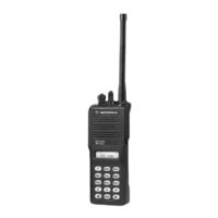
Motorola MTX series Service Manual (146 pages)
Professional Series Two-Way Portable Radios
Brand:
Motorola
| Category:
Portable Radio
| Size: 2.27 MB
Table of Contents
Table of Contents
7
Foreword
6
Manual Revisions
6
Computer Software Copyrights
6
Document Copyrights
6
Disclaimer
6
Trademarks
6
Table of Contents
7
List of Figures
15
Chapter 9 Schematic Diagrams, Overlays, and Parts Lists
15
Keypad-Controller Interconnect Flex Schematic
15
List of Figures
15
UHF Band
18
Intrinsically Safe Radio Information
23
FMRC Approved Equipment
23
Relabeling
24
Repair
24
Repair of FMRC Approved Products
24
Do Not Substitute Options or Accessories
25
Chapter 1 Introduction
27
Scope of Manual
27
Warranty and Service Support
27
After Warranty Period
27
Return Instructions
27
Warranty Period
27
Related Documents
28
Technical Support
28
Piece Parts Availability
28
Radio Model Chart and Specifications
29
Radio Model Information
29
Chapter 2 Radio Power Distribution
31
Figure 2-1. DC Power Distribution Block Diagram
31
Chapter 3 Keypad
33
Controller Board
33
Figure 3-1. Keypad Block Diagram
33
Figure 3-2. Controller Block Diagram
34
MCU Digital
34
Real Time Clock
34
Circuit Description
35
Figure 3-3. RTC Circuit
35
MODB/VSTBY Supply
35
Audio/Signaling
36
Chapter 4 UHF Band 1 Theory of Operation
37
Transmitter
37
Figure 4-1. Transmitter Block Diagram
37
General
37
Power Amplifier
37
Antenna Matching Network
38
Antenna Switch
38
Harmonic Filter
38
Power Control Integrated Circuit (PCIC)
38
Receiver
39
Figure 4-2. UHF Receiver Block Diagram
39
Receiver Front-End
39
Receiver Back-End
40
Frequency Generation Circuitry
40
Figure 4-3. Frequency Generation Unit Block Diagram
40
Synthesizer
41
Figure 4-4. Synthesizer Block Diagram
41
Voltage-Controlled Oscillator (VCO)
42
Figure 4-5. VCO Block Diagram
42
Chapter 5 UHF Band 2 Theory of Operation
45
Transmitter
45
Figure 5-1. Transmitter Block Diagram
45
General
45
Power Amplifier
45
Antenna Matching Network
46
Antenna Switch
46
Harmonic Filter
46
Power Control Integrated Circuit (PCIC)
46
Receiver
47
Figure 5-2. UHF Receiver Block Diagram
47
Receiver Front-End
47
Receiver Back-End
48
Frequency Generation Circuitry
48
Figure 5-3. Frequency Generation Unit Block Diagram
48
Synthesizer
49
Figure 5-4. Synthesizer Block Diagram
49
Voltage-Controlled Oscillator (VCO)
50
Figure 5-5. VCO Block Diagram
50
Chapter 6 VHF Theory of Operation
53
Transmitter
53
Figure 6-1. Transmitter Block Diagram
53
General
53
Power Amplifier
53
Antenna Matching Network
54
Antenna Switch
54
Harmonic Filter
54
Power Control Integrated Circuit (PCIC)
54
Receiver (for All Models Except those with PCB 8486473Z04)
55
Figure 6-2. VHF Receiver Block Diagram
55
Receiver Front-End
55
Automatic Gain Control Circuit
56
Receiver Back-End
56
Receiver (for Models with PCB 8486473Z04)
57
Figure 6-3. VHF Receiver Block Diagram
57
Receiver Back-End
58
Receiver Front-End
58
Automatic Gain Control Circuit
59
Frequency Generation Circuitry
60
Figure 6-4. Frequency Generation Unit Block Diagram
60
Synthesizer
61
Figure 6-5. Synthesizer Block Diagram
61
Voltage-Controlled Oscillator (VCO)
62
Figure 6-6. VCO Block Diagram
62
Chapter 7 Low Band, 800 Mhz, Passport & 900 Mhz Theory of Operation
65
Introduction
65
Low Band Transmitter
65
Figure 7-1. Low Band Transmitter Block Diagram
65
Power Amplifier (PA)
65
Antenna Matching Transformer
66
Antenna Switch
66
Electrostatic Discharge (ESD) Protection Circuit
66
Harmonic Filter
66
Power Control Integrated Circuit (PCIC)
66
Temperature Cut Back Circuit
66
Low Band Receiver
67
Figure 7-2. Low Band Receiver Block Diagram
67
Receiver Front-End
67
Automatic Gain Control (AGC)
68
Frequency Generation Circuit
68
Receiver Back-End
68
Synthesizer
69
Figure 7-3. Low Band Frequency Generation Unit Block Diagram
69
Voltage Control Oscillators (VCO)
70
Buffer
70
Figure 7-4. Low Band Synthesizer Block Diagram
70
Receive VCO
70
Transmit VCO
70
Diplexer/Output Filters
71
Prescalar Feedback
71
800 Mhz Transmitter
71
Figure 7-5. 800 Mhz Transmitter Block Diagram
71
Power Amplifier
71
Antenna Switch
72
Harmonic Filter
72
Power Control Integrated Circuit (PCIC)
72
800 Mhz Receiver
73
Figure 7-6. 800 Mhz Receiver Block Diagram
73
Receiver Front-End
73
Automatic Gain Control Circuit
74
Receiver Back-End
74
Figure 7-7. 800 Mhz Frequency Generation Unit Block Diagram
75
Frequency Generation Circuit
75
Synthesizer
76
Figure 7-8. 800 Mhz Synthesizer Block Diagram
76
Figure 7-9. 800 Mhz VCO Block Diagram
77
Voltage Control Oscillator (VCO)
77
Trunked Radio Systems
78
LTR™ Trunked Systems
78
MPT Trunked Systems
78
Privacy Plus Trunked Systems
78
Keyboard Circuit
79
Low Speed Data Filter
79
Microcontroller (MCU)
79
Passport™ Trunked Systems
79
Power Supplies
79
Backlight Driver and Led's
80
Voice Storage
80
900 Mhz Transmitter
80
Figure 7-10. Transmitter Block Diagram
80
Antenna Switch
81
Harmonic Filter
81
Power Amplifier
81
Power Control Integrated Circuit (PCIC)
81
900 Mhz Receiver
82
Figure 7-11. 900 Mhz Receiver Block Diagram
82
Receiver Front-End
82
Hear Clear IC
83
Receiver Back-End
83
Automatic Gain Control Circuit
84
Hear Clear Routing of Data/Signaling
84
Receive Path for Radios with Hear Clear
84
Frequency Generation Circuitry
85
Figure 7-12. Frequency Generation Unit Block Diagram
85
900 Mhz Synthesizer
86
Figure 7-13. Synthesizer Block Diagram
87
900 Mhz Voltage Control Oscillator (VCO)
88
Figure 7-14. VCO Block Diagram
88
Chapter 8 Maintenance
91
Introduction
91
Preventive Maintenance
91
Inspection
91
Cleaning
91
Safe Handling of CMOS and LDMOS
92
General Repair Procedures and Techniques
92
Recommended Test Tools
94
Replacing the Circuit Board Fuse
95
Figure 8-1. Uhf/Vhf/Low Band/800 Mhz/900 Mhz Circuit Board Fuse Locations
96
Removing and Reinstalling the Circuit Board
97
Power up Self-Test Error Codes
97
Figure 8-2. Circuit Board Removal and Reinstallation
97
UHF Band 1 Troubleshooting Charts
99
Troubleshooting Flow Chart for Controller for All Models Except
99
Troubleshooting Flow Chart for Controller for Models with PCB 8486458Z03
100
PCB 8486458Z03 (Sheet 1 of 2)
101
Troubleshooting Flow Chart for Receiver for All Models Except
101
PCB 8486458Z03 (Sheet 2 of 2)
102
Troubleshooting Flow Chart for Receiver for All Models Except
102
Troubleshooting Flow Chart for Receiver, for Models with PCB 8486458Z03 (Sheet 1 of 2)
103
Troubleshooting Flow Chart for Receiver, for Models with PCB 8486458Z03 (Sheet 2 of 2)
104
Troubleshooting Flow Chart for Transmitter
105
Troubleshooting Flow Chart for Synthesizer
106
Troubleshooting Flow Chart for VCO
107
UHF Band 2 Troubleshooting Charts
108
Pcb 8486686Z02
108
Troubleshooting Flow Chart for Controller for All Models
108
Troubleshooting Flow Chart for Controller for Models with PCB 8486686Z02
109
Troubleshooting Flow Chart for Receiver, for All Models Except those with PCB 8486686Z02 (Sheet 1 of 2)
110
Troubleshooting Flow Chart for Receiver, for All Models Except those with PCB 8486686Z02 (Sheet 2 of 2)
111
Troubleshooting Flow Chart for Receiver, for Models with PCB 8486686Z02 (Sheet 1 of 2)
112
Troubleshooting Flow Chart for Receiver, for Models with PCB 8486686Z02 (Sheet 2 of 2)
113
Troubleshooting Flow Chart for Transmitter
114
Troubleshooting Flow Chart for Synthesizer
115
Troubleshooting Flow Chart for VCO
116
VHF Troubleshooting Charts
117
Troubleshooting Flow Chart for Controller for All Models
117
Troubleshooting Flow Chart for Controller for Models with PCB 8486473Z04
118
Except those with PCB 8486473Z04
119
Troubleshooting Flow Chart for Receiver, for All Models
119
Troubleshooting Flow Chart for Receiver, for All Models Except those with PCB 8486473Z04 (Sheet 1 of 2)
119
Troubleshooting Flow Chart for Receiver, for All Models Except those with PCB 8486473Z04 (Sheet 2 of 2)
120
Troubleshooting Flow Chart for Receiver for Models with PCB 8486473Z04 (Sheet 1 of 2)
121
Troubleshooting Flow Chart for Receiver for Models with PCB 8486473Z04 (Sheet 2 of 2)
122
Troubleshooting Flow Chart for Transmitter
123
Troubleshooting Flow Chart for Synthesizer
124
Troubleshooting Flow Chart for VCO
125
Low Band Troubleshooting Charts
126
Troubleshooting Flow Chart for Controller
126
Troubleshooting Flow Chart for Receiver (Sheet 1 of 2)
127
Troubleshooting Flow Chart for Receiver (Sheet 2 of 2)
128
Troubleshooting Flow Chart for Transmitter
129
Troubleshooting Flow Chart for Synthesizer
130
Troubleshooting Flow Chart for VCO
131
800 Mhz Troubleshooting Charts
132
Troubleshooting Flow Chart for Controller
132
Troubleshooting Flow Chart for Receiver (Sheet 1 of 2)
133
Troubleshooting Flow Chart for Receiver (Sheet 2 of 2)
134
Troubleshooting Flow Chart for Transmitter
135
Troubleshooting Flow Chart for Synthesizer
136
Troubleshooting Flow Chart for VCO
137
Passport Trunking Troubleshooting Chart
138
Keypad Troubleshooting Chart
139
Mhz Troubleshooting Charts
140
Troubleshooting Flow Chart for Controller (Sheet 2 of 2)
141
Troubleshooting Flow Chart for Receiver (Sheet 1 of 2)
142
Troubleshooting Flow Chart for Receiver (Sheet 2 of 2)
143
Troubleshooting Flow Chart for VCO
146
Advertisement
Motorola MTX series Detailed Service Manual (96 pages)
Professional Series Two-Way Portable Radios
Brand:
Motorola
| Category:
Two-Way Radio
| Size: 2.32 MB
Table of Contents
Revision Change
1
Fmr-2045A
2
Table of Contents
3
Chapter 1 UHF Theory of Operation
7
Transmitter
7
General
7
Power Amplifier
7
Transmitter Block Diagram
7
Antenna Switch
8
Harmonic Filter
8
Antenna Matching Network
8
Power Control Integrated Circuit (PCIC)
8
Receiver
9
Receiver Front-End
9
UHF Receiver Block Diagram
9
Receiver Back-End
10
Frequency Generation Circuitry
10
Frequency Generation Unit Block Diagram
10
Synthesizer
11
Synthesizer Block Diagram
11
Voltage-Controlled Oscillator (VCO)
12
VCO Block Diagram
12
Chapter 2 UHF Circuit Board Layouts, Schematic Diagrams and Parts List
15
Notes for All Schematics and Circuit Boards
15
Circuit Board/Schematic Diagrams and Parts List
17
UHF (403-470Mhz) Main Board Top Side PCB No. 8486458Z02
17
UHF (403-470Mhz) Main Board Bottom Side PCB No. 8486458Z02
18
UHF Controls and Switches Schematic Diagram
19
UHF Receiver Front-End Schematic Diagram
20
UHF Receiver Back-End Schematic Diagram
21
UHF Synthesizer Schematic Diagram
22
UHF Voltage Controlled Oscillator Schematic Diagram
23
UHF Harmonic Filter Schematic Diagram
24
UHF Transmitter Schematic Diagram
25
Controller ASFIC/ON_OFF Schematic Diagram
30
Chapter 3 UHF Troubleshooting Charts
31
Troubleshooting Flow Chart for Controller
31
Troubleshooting Flow Chart for Receiver (Sheet 1 of 2)
32
Troubleshooting Flow Chart for Receiver (Sheet 2 of 2)
33
Troubleshooting Flow Chart for Transmitter
34
Troubleshooting Flow Chart for Synthesizer
35
Troubleshooting Flow Chart for VCO
36
Chapter 4 UHF Band 2 Theory of Operation
37
Transmitter
37
General
37
Power Amplifier
37
Transmitter Block Diagram
37
Antenna Switch
38
Harmonic Filter
38
Antenna Matching Network
38
Power Control Integrated Circuit (PCIC)
38
Receiver
39
Receiver Front-End
39
UHF Receiver Block Diagram
39
UHF Band 2 Receiver Front End Schematic Diagram
39
Receiver Back-End
40
Frequency Generation Circuitry
40
Frequency Generation Unit Block Diagram
40
UHF Band 2 Receiver Back End Schematic Diagram
40
Synthesizer
41
Synthesizer Block Diagram
41
Voltage-Controlled Oscillator (VCO)
42
VCO Block Diagram
42
Chapter 5 UHF Band 2 CB Layouts, Schematic Diagrams, and Parts List
45
Notes for All Schematics and Circuit Boards
45
Circuit Board/Schematic Diagrams and Parts List
47
UHF Band 2 (450-527 Mhz) Main Board Top Side PCB No. 8486686Z01
47
UHF Band 2 (450-527 Mhz) Main Board Bottom Side PCB No. 8486686Z01
48
UHF Band 2 Synthesizer Schematic Diagram
52
UHF Band 2 Voltage Controlled Oscillator Schematic Diagram
53
UHF Band 2 Harmonic Filter Schematic Diagram
54
UHF Band 2 Transmitter Schematic Diagram
55
Controller ASFIC/ON_OFF Schematic Diagram
60
Chapter 6 UHF Band 2 Troubleshooting Charts
61
Troubleshooting Flow Chart for Controller
61
Troubleshooting Flow Chart for Receiver (Sheet 1 of 2)
62
Troubleshooting Flow Chart for Receiver (Sheet 2 of 2)
63
Troubleshooting Flow Chart for Transmitter
64
Troubleshooting Flow Chart for Synthesizer
65
Troubleshooting Flow Chart for VCO
66
Motorola MTX series Theory/Troubleshooting Manual (60 pages)
Handie-Talkie Portable Radios
Brand:
Motorola
| Category:
Portable Radio
| Size: 14.71 MB
Table of Contents
Table of Contents
5
Glossary of Terms
8
Introduction
9
Description
9
General
9
Printed Circuit Boards and Flexible Circuits
9
Theory of Operation (Basic Functional Description)
10
Purpose
9
Introduction
10
Radio Power
10
B+ Routing and DC Voltage Distribution
10
VHF or UHF Transceiver)
10
800 Or 900Mhz Transceiver)
10
General
10
Antenna Switch
12
Frequency Generation Unit (See Figure 2)
12
Receiver Front End (See Figure 3)
12
Receiver Back End (See Figure 3)
13
Transmitter (See Figure 4)
13
Vhf/Uhf Transceiver Board
12
800/900Mhz TRANSCEIVER BOARD
14
Antenna Switch
14
Frequency Generation Unit (See Figure 5)
14
Receiver Front End (See Figure 6)
14
Receiver Back End (See Figure 6)
15
Transmitter (See Figure 7)
15
Closed Architecture Controller
16
Audio Signalling Architecture
16
Digital Architecture
16
General (See Figure 8)
16
General (See Figure 9)
16
Audio Signalling Architecture
17
Digital Architecture
17
Theory of Operation (Detailed Functional Description)
18
Open Architecture Controller
16
Introduction
18
Radio Power
18
General
18
And a VHF or UHF Transceiver)
18
B+ Routing and DC Voltage Distribution
19
And an 800 or 900Mhz Transceiver)
19
Vhf/Uhf Transceiver
20
Frequency Generation Unit (FGU)
20
Antenna Switch
21
Receiver Front End
21
Receiver Back End
22
Transmitter
22
800/900Mhz TRANSCEIVER BOARD
23
Frequency Synthesis
23
Antenna Switch
24
Receiver Front End
24
Receiver Back End
25
Transmitter
25
Closed Architecture Controller
25
Microcomputer (U705)
25
Controller Board Circuit Operation
27
Open Architecture Controller
29
Microprocessor (U705) and Associated Circuits
30
Controller Board Circuit Operation
32
UNIVERSAL CONNECTOR (See Tables 2 and 3)
36
Motorola MTX series Service Manual (66 pages)
Handie-Talkie Portable Radios
Brand:
Motorola
| Category:
Portable Radio
| Size: 0.49 MB
Table of Contents
Table of Contents
2
Model Numbering System
5
List of Models
6
List of Antennas and Batteries
7
Maintenance Specifications for Vhf Radios
8
Maintenance Specifications for Uhf Radios
8
MAINTENANCE SPECIFICATIONS for 800Mhz RADIOS
9
MAINTENANCE SPECIFICATIONS for 900Mhz RADIOS
9
Section I. Introduction
10
Service Aids
11
Recommended and Required Test Equipment, Service Aids, and Tools Lists
11
Recommended Test Equipment
11
Service Aids and Recommended Tools
11
Field Programming
11
Recommended Service Tools
13
Initial Equipment Control Settings
14
Test Environments, HT 1000 Radios
14
Section III. Transceiver Performance Testing
14
General
14
Setup
14
Test Mode
14
Test Frequencies, HT 1000 Radios
15
Test Environments, MT 2000, MTS 2000, and MTX Series Radios
16
Receiver Performance Checks
17
Transmitter Performance Checks
18
Error Code Displays
19
Power-Up Display Codes
19
Operational Display Codes
19
Section V. Radio Alignment Procedure
20
General
20
Reference Oscillator Alignment
22
Front-End Pre-Selector (VHF/UHF Only)
22
Rated Audio
22
Squelch
22
Standard Test Modulation (1Khz Tone)
22
Transmitter Power
23
Transmit Deviation Balance (Compensation)
23
Transmit Deviation Limit
23
Transmit Power Setting
23
Transmit Deviation Limit Reference
24
VCO Crossover Frequency
24
Signalling Deviation
24
Transmit Deviation Limit
24
Section VI. Disassembly and Reassembly
26
General
26
Disassembly to Board Level
26
Disassembly of Control Top
28
Disassembly of Front Cover Assembly
29
Reassembly
30
Section VII. Maintenance
32
Introduction
32
Preventive Maintenance
32
Safe Handling of CMOS Devices
32
Repair Procedures and Techniques
32
Nud7070A, Nud7070B, Nud7085A, and Nud7085B Vhf Transceiver Boards' Component Location Diagrams and Schematic Diagram
38
Transceiver Boards' Component Location Diagrams
39
Motorola MTX series Service Manual (122 pages)
Professional Series Two-Way Portable Radio
Brand:
Motorola
| Category:
Two-Way Radio
| Size: 3.25 MB
Table of Contents
Swb
19
VDDD
19
Int_Ext_Vdd
19
Key_Int
20
VDDD
21
Table of Contents
105
Ptt
119
Vs_Int
119
Reset
119
Pg7_R_W
119
Gnd
119
Advertisement
Related Products
Motorola MTX850 LS
Motorola MTX-900 Classic
Motorola MTX-800 Classic
Motorola MTX-810
Motorola MTX-LS
Motorola MTX1500
Motorola MTX4500
Motorola Handie-Talkie MTX 2000
Motorola IMPRES Tetra MTP700
Motorola ASTRO MT 1500
MOTOROLA Categories
Cell Phone
Two-Way Radio
Baby Monitor
Cordless Telephone
Radio
More MOTOROLA Manuals
Login
Sign In
OR
Sign in with Facebook
Sign in with Google
Upload manual
Upload from disk
Upload from URL