Sign In
Upload
Manuals
Brands
Motorola Manuals
Portable Radio
ASTRO XTS 2250
Motorola ASTRO XTS 2250 Manuals
Manuals and User Guides for Motorola ASTRO XTS 2250. We have
2
Motorola ASTRO XTS 2250 manuals available for free PDF download: Service Manual, Basic Service Manual
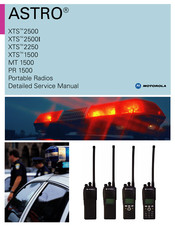
Motorola ASTRO XTS 2250 Service Manual (817 pages)
Brand:
Motorola
| Category:
Portable Radio
| Size: 44.21 MB
Table of Contents
Foreword
2
Safety Information
2
Manual Revisions
2
Computer Software Copyrights
2
Documentation Copyrights
2
Disclaimer
2
Trademarks
2
Document History
3
Table of Contents
5
Chapter 1 Introduction
25
General
25
Notations Used in this Manual
25
Chapter 2.1 VHF Overall Characteristics
27
Introduction
27
Analog Mode of Operation-Receiving
27
Analog Mode of Operation-Transmitting
28
ASTRO Mode (Digital Mode) of Operation
28
Main Board Overview
28
Vocoder Circuitry Overview
29
Chapter 2.2 UHF1 Overall Characteristics
31
Introduction
31
Analog Mode of Operation-Receiving
31
Analog Mode of Operation-Transmitting
32
ASTRO Mode (Digital Mode) of Operation
32
Main RF Board Overview
32
Vocoder Circuitry Overview
33
Chapter 2.3 UHF2 Overall Characteristics
35
Introduction
35
Analog Mode of Operation-Receiving
35
Analog Mode of Operation-Transmitting
36
ASTRO Mode (Digital Mode) of Operation
36
Main RF Board Overview
36
Vocoder Circuitry Overview
37
Chapter 2.4 700/800 Mhz Overall Characteristics
39
Introduction
39
Analog Mode of Operation-Receiving
39
Analog Mode of Operation-Transmitting
40
ASTRO Mode (Digital Mode) of Operation
40
Main Board Overview
40
Vocoder Circuitry Overview
41
Chapter 2.5 900Mhz Overall Characteristics
43
Introduction
43
Analog Mode of Operation-Receiving
43
Analog Mode of Operation-Transmitting
44
ASTRO Mode (Digital Mode) of Operation
44
Main Board Overview
44
Vocoder Circuitry Overview
45
Chapter 3.1 VHF Radio Power
47
Introduction
47
Radio Power up or down
47
General
47
B+ Routing for VHF Band Main Board
48
Figure 3.1-1.B+ Routing for VHF Main Board
48
B+ and +5V Routing for VOCON
49
Figure 3.1-2.XTS 2500/XTS 2500I DC Distribution (for All Other Kits)
49
Table 3.1-1. Power Supply Configuration for VOCON Section
50
Chapter 3.2 UHF1 Radio Power
51
Introduction
51
Radio Power up or down
51
General
51
B+ Main Board Routing
52
Figure 3.2-1.B+ Routing for Main Board
52
B+ and +5V Routing for VOCON
53
Figure 3.2-2.XTS 2500/XTS 2500I DC Distribution (for All Other Kits)
53
Table 3.2-1. Power Supply Configuration for VOCON Section
54
Chapter 3.3 UHF2 Radio Power
55
Introduction
55
Radio Power up or down
55
General
55
B+ Routing for UHF2 Band Main Board
56
Figure 3.3-1.B+ Routing for Main Board
56
B+ and +5V Routing for VOCON
57
Figure 3.3-2.XTS 2500/XTS 2500I DC Distribution (for All Other Kits)
57
Table 3.3-1. Power Supply Configuration for VOCON Section
58
Chapter 3.4 700/800 Mhz Radio Power
59
Introduction
59
Radio Power up or down
59
General
59
B+ Routing for 700/800 Mhz Band Main Board
60
Figure 3.4-1.B+ Routing for 700/800 Mhz Main Board
60
B+ and +5V Routing for VOCON
61
Figure 3.4-2.XTS 2500/XTS 2500I DC Distribution (for All Other Kits)
61
Table 3.4-1. Power Supply Configuration for VOCON Section
62
Chapter 3.5 900 Mhz Radio Power
63
Introduction
63
Radio Power up or down
63
General
63
B+ Routing for 900 Mhz Band Main Board
64
Figure 3.5-1.B+ Routing for 900Mhz Main Board
64
B+ and +5V Routing for VOCON
65
Figure 3.5-2.XTS 2500/XTS 2500I DC Distribution (for All Other Kits)
65
Table 3.5-1. Power Supply Configuration for VOCON Section
66
Chapter 4.1 VHF Detailed Theories of Operation
67
Introduction
67
Frequency Synthesis
67
Antenna Switch
68
Receiver
68
Front End
69
Back End
69
Transmitter
70
VOCON Functional Blocks
71
Controller and Memory Section
71
Patriot IC (U800)
71
Flash Memory (U803)
74
Sram (U804)
74
Figure 4.1-1.Controller Memory Interface
75
Audio and Power Section
76
Mako IC (U701)
76
Audio Power Amplifier
77
Audio Pre-Amplifier
77
Regulator
77
Interface Support Section
78
Mako IC U701
78
ESD Protection Circuitry
79
Universal Connector (Side Connector) Interface Circuitry
79
Figure 4.1-2.Universal (Side) Connector
80
Figure 4.1-3.VOCON Connector J650
80
Table 4.1-1. Option Select Functions
80
The Option Board
81
Encryption Module
82
Table 4.1-2. Encryption Module Software Kits and Algorithms
82
System Clocks
83
Transmit Audio Path
83
Figure 4.1-4.VOCON Transmit Audio Path
83
Receive Audio Path
84
Figure 4.1-5.VOCON Receive Audio Path
84
Chapter 4.2 UHF1 Detailed Theories of Operation
85
Introduction
85
Frequency Synthesis
85
Antenna Switch
86
Receiver
87
Front End
87
Back End
88
Transmitter
88
VOCON Functional Blocks
89
Controller and Memory Section
89
Patriot IC (U800)
89
Sram (U804)
92
Figure 4.2-1.Controller Memory Interface
93
Flash Memory (U803)
93
Audio and Power Section
94
Mako IC (U701)
94
Audio Power Amplifier
95
Audio Pre-Amplifier
95
Regulator
95
Interface Support Section
96
Mako IC U701
96
ESD Protection Circuitry
97
Universal Connector (Side Connector) Interface Circuitry
97
Figure 4.2-2.Universal (Side) Connector
98
Figure 4.2-3.VOCON Connector J650
98
Table 4.2-1. Option Select Functions
98
The Option Board
99
Encryption Module
100
Table 4.2-2. Encryption Module Software Kits and Algorithms
100
Figure 4.2-4.VOCON Transmit Audio Path
101
System Clocks
101
Transmit Audio Path
101
Figure 4.2-5.VOCON Receive Audio Path
102
Receive Audio Path
102
Chapter 4.3 UHF2 Detailed Theories of Operation
103
Introduction
103
Frequency Synthesis
103
Antenna Switch
104
Receiver
105
Front End
105
Back End
106
Transmitter
106
VOCON Functional Blocks
107
Controller and Memory Section
107
Patriot IC (U800)
107
Flash Memory (U803)
110
Sram (U804)
110
Figure 4.3-1.Controller Memory Interface
111
Audio and Power Section
112
Mako IC (U701)
112
Audio Power Amplifier
113
Audio Pre-Amplifier
113
Regulator
113
Interface Support Section
114
Mako IC U701
114
ESD Protection Circuitry
115
Universal Connector (Side Connector) Interface Circuitry
115
Figure 4.3-2.Universal (Side) Connector
116
Figure 4.3-3.VOCON Connector J650
116
Table 4.3-1. Option Select Functions
116
The Option Board
117
Encryption Module
118
Table 4.3-2. Encryption Module Software Kits and Algorithms
118
Figure 4.3-4.VOCON Transmit Audio Path
119
System Clocks
119
Transmit Audio Path
119
Figure 4.3-5.VOCON Receive Audio Path
120
Receive Audio Path
120
Chapter 4.4 700/800 Mhz Detailed Theories of Operation
121
Introduction
121
Frequency Synthesis
121
Antenna Switch
122
Receiver
123
Front End
123
Back End
124
Transmitter
124
VOCON Functional Blocks
125
Controller and Memory Section
125
Patriot IC (U800)
125
Flash Memory (U803)
128
Sram (U804)
128
Figure 4.4-1.Controller Memory Interface
129
Audio and Power Section
130
Mako IC (U701)
130
Audio Power Amplifier
131
Audio Pre-Amplifier
131
Regulator
131
Interface Support Section
132
Mako IC U701
132
ESD Protection Circuitry
133
Universal Connector (Side Connector) Interface Circuitry
133
Figure 4.4-2.Universal (Side) Connector
134
Figure 4.4-3.VOCON Connector J650
134
Table 4.4-1. Option Select Functions
134
The Option Board
135
Encryption Module
136
Table 4.4-2. Encryption Module Software Kits and Algorithms
136
System Clocks
137
Transmit Audio Path
137
Figure 4.4-4.VOCON Transmit Audio Path
138
Receive Audio Path
138
Figure 4.4-5.VOCON Receive Audio Path
139
Chapter 4.5 900 Mhz Detailed Theories of Operation
141
Introduction
141
Frequency Synthesis
141
Antenna Switch
142
Receiver
143
Front End
143
Back End
144
Transmitter
144
VOCON Functional Blocks
145
Controller and Memory Section
145
Patriot IC (U800)
145
Flash Memory (U803)
148
Sram (U804)
148
Figure 4.5-1.Controller Memory Interface
149
Audio and Power Section
150
Mako IC (U701)
150
Audio Power Amplifier
151
Audio Pre-Amplifier
151
Interface Support Section
151
Regulator
151
Mako IC U701
152
ESD Protection Circuitry
153
Universal Connector (Side Connector) Interface Circuitry
153
Figure 4.5-2.Universal (Side) Connector
154
Figure 4.5-3.VOCON Connector J650
154
Table 4.5-1. Option Select Functions
154
The Option Board
154
Encryption Module
156
Table 4.5-2. Encryption Module Software Kits and Algorithms
156
Figure 4.5-4.VOCON Transmit Audio Path
157
System Clocks
157
Transmit Audio Path
157
Figure 4.5-5.VOCON Receive Audio Path
158
Receive Audio Path
158
Chapter 5 Troubleshooting Procedures
159
Introduction
159
Handling Precautions
159
Voltage Measurement and Signal Tracing
159
Standard Bias Table
160
Table 5-1. Standard Operating Bias
160
Power-Up Self-Check Errors
161
Table 5-2. Power-Up Self-Check Error Codes
161
Operational Error Codes
162
Power-Up, Self-Check Diagnostics, and Repair (Not for Field Use)
162
Table 5-3. Operational Error Code Displays
162
Table 5-4. Additional Error Code Action Items
162
Chapter 6.1 VHF Troubleshooting Charts
165
Introduction
165
List of Troubleshooting Flowcharts
165
VHF Radio Main Troubleshooting Chart
166
Radio Power-Up Fail Troubleshooting Chart (1 of 3)
167
Radio Power-Up Fail Troubleshooting Chart (2 of 3)
168
Radio Power-Up Fail Troubleshooting Chart (3 of 3)
169
DC Supply Fail Troubleshooting Chart (1 of 3)
170
DC Supply Fail Troubleshooting Chart (2 of 3)
171
Volume Set Error Troubleshooting Chart
174
Top/Side Button Error Troubleshooting Chart
176
No Display Troubleshooting Chart (1 of 3)
177
VOCON Transmit Audio Troubleshooting Chart (1 of 2)
183
VOCON Transmit Audio Troubleshooting Chart (2 of 2)
184
No Transmit Deviation Troubleshooting Chart
185
Secure Hardware Failure
187
Chapter 6.2 UHF1 Troubleshooting Charts
189
Introduction
189
List of Troubleshooting Flowcharts
189
UHF Range 1 Radio Main Troubleshooting Chart
190
Radio Power-Up Fail Troubleshooting Chart (1 of 3)
191
Radio Power-Up Fail Troubleshooting Chart (2 of 3)
192
Radio Power-Up Fail Troubleshooting Chart (3 of 3)
193
DC Supply Fail Troubleshooting Chart (1 of 3)
194
DC Supply Fail Troubleshooting Chart (2 of 3)
195
DC Supply Fail Troubleshooting Chart (3 of 3)
196
Button Test Troubleshooting Chart
213
Volume Set Error Troubleshooting Chart
213
Zone/Channel Select Error Troubleshooting Chart
213
Top/Side Button Error Troubleshooting Chart
213
VOCON Receive Audio Troubleshooting Chart
213
No Transmit Deviation Troubleshooting Chart
213
Secure Hardware Failure
213
Chapter 6.3 UHF2 Troubleshooting Charts
213
Introduction
213
List of Troubleshooting Flowcharts
213
UHF Range 2 Radio Main Troubleshooting Chart
214
Radio Power-Up Fail Troubleshooting Chart (1 of 3)
215
Radio Power-Up Fail Troubleshooting Chart (2 of 3)
216
Radio Power-Up Fail Troubleshooting Chart (3 of 3)
217
DC Supply Fail Troubleshooting Chart (1 of 3)
218
DC Supply Fail Troubleshooting Chart (2 of 3)
219
Volume Set Error Troubleshooting Chart
222
Zone/Channel Select Error Troubleshooting Chart
223
Top/Side Button Error Troubleshooting Chart
224
No Display Troubleshooting Chart (1 of 3)
225
No Display Troubleshooting Chart (2 of 3)
226
VOCON Transmit Audio Troubleshooting Chart (1 of 2)
231
VOCON Transmit Audio Troubleshooting Chart (2 of 2)
232
No Transmit Deviation Troubleshooting Chart
233
Secure Hardware Failure
235
Chapter 6.4 700/800 Mhz Troubleshooting Charts
237
Introduction
237
List of Troubleshooting Flowcharts
237
700/800 Mhz Radio Main Troubleshooting Chart
238
Radio Power-Up Fail Troubleshooting Chart (1 of 3)
239
Radio Power-Up Fail Troubleshooting Chart (2 of 3)
240
Radio Power-Up Fail Troubleshooting Chart (3 of 3)
241
DC Supply Fail Troubleshooting Chart (1 of 3)
242
DC Supply Fail Troubleshooting Chart (2 of 3)
243
DC Supply Fail Troubleshooting Chart (3 of 3)
244
Volume Set Error Troubleshooting Chart
246
Top/Side Button Error Troubleshooting Chart
261
VOCON Receive Audio Troubleshooting Chart
261
No Transmit Deviation Troubleshooting Chart
261
Secure Hardware Failure
261
Chapter 6.5 900 Mhz Troubleshooting Charts
261
Introduction
261
List of Troubleshooting Flowcharts
261
900 Mhz Radio Main Troubleshooting Chart
262
Radio Power-Up Fail Troubleshooting Chart (1 of 3)
263
Radio Power-Up Fail Troubleshooting Chart (2 of 3)
264
Radio Power-Up Fail Troubleshooting Chart (3 of 3)
265
DC Supply Fail Troubleshooting Chart (1 of 3)
266
DC Supply Fail Troubleshooting Chart (2 of 3)
267
Volume Set Error Troubleshooting Chart
270
Top/Side Button Error Troubleshooting Chart
272
No Display Troubleshooting Chart (1 of 3)
273
No Display Troubleshooting Chart (2 of 3)
274
No Display Troubleshooting Chart (3 of 3)
275
900 Mhz Receive RF Troubleshooting Chart
276
VOCON Receive Audio Troubleshooting Chart
277
VOCON Transmit Audio Troubleshooting Chart (1 of 2)
279
VOCON Transmit Audio Troubleshooting Chart (2 of 2)
280
No Transmit Deviation Troubleshooting Chart
281
Secure Hardware Failure
283
Chapter 7.1 VHF Troubleshooting Waveforms
285
Introduction
285
List of Waveforms
285
Table 7.1-1. List of Waveforms
285
RF Test Points
286
Figure 7.1-1.RF Block Diagram Test Points
286
Table 7.1-2. RF Block Diagram Probe/Test Points
287
Main Circuit Board RF Shield Locations
288
Table 7.1-3. Main Circuit Board Side 1 RF Shields
288
Table 7.1-4. Main Circuit Board Side 2 RF Shields
289
PP1 Antenna Input
290
PP2 TX Signal at Harmonic Filter Input
291
PP3 Coupler RF out
292
PP4 TX Signal at PA
293
TP5 Coupler RF Feedback to PCIC
294
TP6 PCIC Control Voltage
295
Pp7 Tx lo
296
PP8 Higher Level Voltage Multiplier
297
PP9 Superfilter Output
298
PP11 Prescalar Input to Fracn Synthesizer
299
PP12 Reference Crystal Output
300
TP13 Mod in
301
TP14 1St lo Control Voltage
302
PP15 VCO Output
303
PP17 Frequency out (16.8 Mhz)
304
PP18 RX RF Input at Antenna Switch
305
PP19 Antenna Switch Bias
306
PP20 Preselector Tuning Voltage
307
PP22 Analog 5V
308
PP23 Preselector 1 Output
309
PP24 Low-Noise Amplifier Output
310
PP25 Preselector 2 Output
311
PP26 Mixer out (IF)
312
PP27 Crystal Filter out
313
PP28 Abacus Analog 3V
314
PP29 2Nd lo Control Voltage
315
PP30 2Nd lo VCO Buffer Output
316
PP31 Analog 5V DC
317
PP32 Abacus Digital 3V
318
TX Audio 1 Khz Tone
331
Mhz Buffer Input and Output
331
Khz Clock Outputs
331
SPI B Data
331
RX Serial Audio Port (SAP)
331
List of Waveforms
331
Table 7.2-1. List of Waveforms
331
RF Test Points
332
Figure 7.2-1.RF Block Diagram Test Points
332
Table 7.2-2. RF Block Diagram Probe/Test Points
333
Main Circuit Board RF Shield Locations
334
Table 7.2-3. Main Circuit Board Side 1 RF Shields
334
Table 7.2-4. Main Circuit Board Side 2 RF Shields
335
PP1 Antenna Input
336
PP2 TX Signal at Harmonic Filter Input
337
PP3 Coupler RF out
338
PP4 TX Signal at PA
339
TP5 Coupler RF Feedback to PCIC
340
TP6 PCIC Control Voltage
341
Pp7 Tx lo
342
TP14 1St lo Control Voltage
348
PP15 VCO Output
349
PP17 Frequency out (19.2 Mhz)
351
PP26 Mixer out (IF)
359
PP31 Analog 5V DC
364
PP32 Abacus Digital 3V
365
TX Audio 1 Khz Tone
379
Mhz Buffer Input and Output
379
Khz Clock Outputs
379
SPI B Data
379
RX Serial Audio Port (SAP)
379
Introduction
379
List of Waveforms
379
Table 7.3-1. List of Waveforms
379
RF Test Points
380
Figure 7.3-1.RF Block Diagram Test Points
380
Table 7.3-2. RF Block Diagram Probe/Test Points
381
Main Circuit Board RF Shield Locations
382
Table 7.3-3. Main Circuit Board Side 1 RF Shields
382
Table 7.3-4. Main Circuit Board Side 2 RF Shields
383
PP1 Antenna Input
384
PP2 TX Signal at Harmonic Filter Input
385
PP3 Coupler RF out
386
PP4 TX Signal at PA
387
TP5 Coupler RF Feedback to PCIC
388
Pp7 Tx lo
390
PP32 Abacus Digital 3V
412
TX Audio 1 Khz Tone
425
Mhz Buffer Input and Output
425
Khz Clock Outputs
425
SPI B Data
425
RX Serial Audio Port (SAP)
425
Introduction
425
List of Waveforms
425
Table 7.4-1. List of Waveforms
425
RF Test Points
426
Figure 7.4-1.RF Block Diagram Test Points
426
Table 7.4-2. RF Block Diagram Probe/Test Points
427
Main Circuit Board RF Shield Locations
428
Table 7.4-3. Main Circuit Board Side 1 RF Shields
428
Table 7.4-4. Main Circuit Board Side 2 RF Shields
429
PP1 Antenna Input
430
PP2 TX Signal at Harmonic Filter Input
431
PP3 Coupler RF out
432
PP4 TX Signal at PA
433
TP5 Coupler RF Feedback to PCIC
434
Pp7 Tx lo
436
Tp10 Trb
439
PP32 Abacus Digital 3V
461
TX Audio 1 Khz Tone
475
Mhz Buffer Input and Output
475
Khz Clock Outputs
475
SPI B Data
475
RX Serial Audio Port (SAP)
475
Introduction
475
List of Waveforms
475
Table 7.5-1. List of Waveforms
475
RF Test Points
476
Figure 7.5-1.RF Block Diagram Test Points
476
Table 7.5-2. RF Block Diagram Probe/Test Points
477
Main Circuit Board RF Shield Locations
478
Table 7.5-3. Main Circuit Board Side 1 RF Shields
478
Table 7.5-4. Main Circuit Board Side 2 RF Shields
479
PP1 Antenna Input
480
PP2 TX Signal at Harmonic Filter Input
481
PP3 Coupler RF out
482
PP4 TX Signal at PA
483
TP5 Coupler RF Feedback to PCIC
484
Pp7 Tx lo
486
Tp10 Trb
489
SPI B Data
515
PP33 SPI Data
517
PP35 Universal Chip Select
519
TP37 RX SSI Data
521
TP39 RX SSI Frame Sync
523
Introduction
525
Tables
525
Table 8.1-1. Main Board to Keypad Board Flex Assembly (J601)
525
Table 8.1-2. Main Board to Universal (Side) Connector Flex Assembly (J650)
527
Table 8.1-3. FLASH (U803) Pinout
527
Table 8.1-4. SRAM (U804) Pinout
530
Table 8.1-5. Patriot MCU/DSP (U800) Pinout
531
Table 8.1-6. MAKO (U701) Pinout
540
Chapter 8.2 UHF1 Troubleshooting Tables
547
Introduction
547
Tables
547
Table 8.2-1. Main Board to Keypad Board Flex Assembly (J601)
547
Table 8.2-2. Main Board to Universal (Side) Connector Flex Assembly (J650)
549
Table 8.2-3. FLASH (U803) Pinout
549
Table 8.2-4. SRAM (U804) Pinout
552
Table 8.2-5. Patriot MCU/DSP (U800) Pinout
553
Table 8.2-6. MAKO (U701) Pinout
562
Chapter 8.3 UHF2 Troubleshooting Tables
569
Introduction
569
Tables
569
Table 8.3-1. Main Board to Keypad Board Flex Assembly (J601)
569
Table 8.3-2. Main Board to Universal (Side) Connector Flex Assembly (J650)
571
Table 8.3-3. FLASH (U803) Pinout
571
Table 8.3-4. SRAM (U804) Pinout
574
Table 8.3-5. Patriot MCU/DSP (U800) Pinout
575
Table 8.3-6. MAKO (U701) Pinout
584
Chapter 8.4 700/800 Mhz Troubleshooting Tables
591
Introduction
591
Tables
591
Table 8.4-1. Main Board to Keypad Board Flex Assembly (J601)
591
Table 8.4-2. Main Board to Universal (Side) Connector Flex Assembly (J650)
593
Table 8.4-3. FLASH (U803) Pinout
593
Table 8.4-4. SRAM (U804) Pinout
596
Table 8.4-5. Patriot MCU/DSP (U800) Pinout
597
Table 8.4-6. MAKO (U701) Pinout
606
Chapter 8.5 900Mhz Troubleshooting Tables
613
Introduction
613
Tables
613
Table 8.5-1. Main Board to Keypad Board Flex Assembly (J601)
613
Table 8.5-2. Main Board to Universal (Side) Connector Flex Assembly (J650)
615
Table 8.5-3. FLASH (U803) Pinout
615
Table 8.5-4. SRAM (U804) Pinout
618
Table 8.5-5. Patriot MCU/DSP (U800) Pinout
619
Table 8.5-6. MAKO (U701) Pinout
628
Table 9.1-1. VHF Schematics, Board Overlays and Parts Lists
635
Figure 9.1-1.Radio Interconnect Block Diagram
636
Figure 9.1-2.PMLD4303A/ PMLD4303D Top Level Schematic
637
Figure 9.1-3.PMLD4303A/ PMLD4303D Controller Interface Schematic
638
Figure 9.1-4.PMLD4303A/ PMLD4303D Interface and Accessories Schematic
639
Figure 9.1-5.PMLD4303A/ PMLD4303D Side Connector Schematic
640
Figure 9.1-6.PMLD4303A/ PMLD4303D Controller Schematic
641
Figure 9.1-7.PMLD4303A/ PMLD4303D Patriot Bravo (U800) Schematic
642
Figure 9.1-8. PMLD4303A/ PMLD4303D MAKO DC and Audio Schematic - Sheet 1 of 2
643
Figure 9.1-9. PMLD4303A/ PMLD4303D MAKO DC and Audio Schematic - Sheet 2 of 2
644
Figure 9.1-10.PMLD4303A/ PMLD4303D Memory Schematic
645
Figure 9.1-11.PMLD4303A/ PMLD4303D Frequency Generation Unit (FGU) and Digital to Analog
646
Figure 9.1-12. PMLD4303A Frequency Generation Unit (FGU) Schematic - Sheet 1 of 3
647
Figure 9.1-13. PMLD4303D Frequency Generation Unit (FGU) Schematic - Sheet 1 of 3
648
Figure 9.1-14. PMLD4303A/ PMLD4303D Frequency Generation Unit (FGU) Schematic - Sheet 2 of 3
649
Figure 9.1-15. PMLD4303A/ PMLD4303D Frequency Generation Unit (FGU) Schematic - Sheet 3 of 3
650
Figure 9.1-16.PMLD4303A/ PMLD4303D Receiver Front End and DC Schematic
651
Figure 9.1-17.PMLD4303A/ PMLD4303D Receiver Front End Schematic
652
Figure 9.1-18. PMLD4303A/ PMLD4303D Receiver Schematic - Sheet 1 of 4
653
Figure 9.1-19. PMLD4303A/ PMLD4303D Receiver Schematic - Sheet 2 of 4
654
Figure 9.1-20. PMLD4303A/ PMLD4303D Receiver Schematic - Sheet 3 of 4
655
Figure 9.1-21. PMLD4303A/ PMLD4303D Receiver Schematic (Regulators) - Sheet 4 of 4
656
Figure 9.1-22.PMLD4303A/ PMLD4303D RF Schematic
657
Figure 9.1-23.PMLD4303A/ PMLD4303D Transmitter Schematic
658
Figure 9.1-24.PMLD4303A RF Controls Schematic
659
Figure 9.1-25.PMLD4303D RF Controls Schematic
660
Figure 9.1-26. PMLD4303A/ PMLD4303D Main Circuit Board Component Location Detail Side
661
Figure 9.1-27. PMLD4303A/ PMLD4303D Main Circuit Board Component Location Detail Side
662
Table 9.2-1. UHF1 Schematics, Board Overlays and Parts Lists
671
Figure 9.2-1.Radio Interconnect Block Diagram
672
Figure 9.2-2.PMLE2537A/ PMLE2537D Top Level Schematic
673
Figure 9.2-3.PMLE2537A/ PMLE2537D Controller Interface Schematic
674
Figure 9.2-4.PMLE2537A/ PMLE2537D Controller Schematic
675
Figure 9.2-5.PMLE2537A/ PMLE2537D Memory Schematic
676
Figure 9.2-6.PMLE2537A/ PMLE2537D Patriot Bravo (U800) Schematic
677
Figure 9.2-7. PMLE2537A/ PMLE2537D MAKO DC and Audio Schematic - Sheet 1 of 2
678
Figure 9.2-8. PMLE2537A/ PMLE2537D MAKO DC and Audio Schematic - Sheet 2 of 2
679
Figure 9.2-9.PMLE2537A/ PMLE2537D Interface and Accessories Schematic
680
Figure 9.2-10.PMLE2537A/ PMLE2537D Side Connector Schematic
681
Figure 9.2-11.PMLE2537A/ PMLE2537D RF Schematic
682
Figure 9.2-12.PMLE2537A/ PMLE2537D Receiver Front End and DC Schematic
683
Figure 9.2-13.PMLE2537A/ PMLE2537D Receiver Front End Schematic
684
Figure 9.2-14. PMLE2537A/ PMLE2537D Receiver Schematic - Sheet 1 of 4
685
Figure 9.2-15. PMLE2537A/ PMLE2537D Receiver Schematic - Sheet 2 of 4
686
Figure 9.2-16. PMLE2537A/ PMLE2537D Receiver Schematic - Sheet 3 of 4
687
Figure 9.2-17. PMLE2537A/ PMLE2537D Receiver Schematic, Regulators - Sheet 4 of 4
688
Figure 9.2-18.PMLE2537A/ PMLE2537D Frequency Generation Unit (FGU) and Digital to Analog
689
Figure 9.2-19. PMLE2537A Frequency Generation Unit (FGU) Schematic - Sheet 1 of 4
690
Figure 9.2-20. PMLE2537D Frequency Generation Unit (FGU) Schematic - Sheet 1 of 4
691
Figure 9.2-21. PMLE2537A/ PMLE2537D Frequency Generation Unit (FGU) Schematic - Sheet 2 of 4
692
Figure 9.2-22. PMLE2537A/ PMLE2537D Frequency Generation Unit (FGU) Schematic - Sheet 3 of 4
693
Figure 9.2-23. PMLE2537A/ PMLE2537D Frequency Generation Unit (FGU) Schematic - Sheet 4 of 4
694
Figure 9.2-24.PMLE2537A RF Controls Schematic
695
Figure 9.2-25.PMLE2537D RF Controls Schematic
696
Figure 9.2-26.PMLE2537A/ PMLE2537D Transmitter Schematic
697
Figure 9.2-27.PMLE2537A/ PMLE2537D Main Circuit Board Component Location Detail - Top Side
698
Figure 9.2-28.PMLE2537A/ PMLE2537D Main Circuit Board Component Location Detail - Bottom Side
699
Table 9.3-1. UHF2 Schematics, Board Overlays and Parts Lists
711
Figure 9.3-1.PMLE4427A/ PMLE4427B (8416852H01_A)
712
Figure 9.3-2.PMLE4427A Controls
713
Figure 9.3-3.PMLE4427B Controls
714
Figure 9.3-4.PMLE4427A/ PMLE4427B Controller Interface Schematic
715
Figure 9.3-5.PMLE4427A/ PMLE4427B Patriot Bravo Revision Schematic
716
Figure 9.3-6.PMLE4427A/ PMLE4427B Digital to Analog Schematic
717
Figure 9.3-7.PMLE4427A/ PMLE4427B Frequency Generation Unit (FGU) Schematic
718
Figure 9.3-8.PMLE4427A/ PMLE4427B Interface and Accessories Schematic
719
Figure 9.3-9.PMLE4427A/ PMLE4427B LNA Schematic
720
Figure 9.3-10. PMLE4427A/ PMLE4427B MAKO Schematic - Sheet 1 of 2
721
Figure 9.3-11. PMLE4427A/ PMLE4427B MAKO Schematic - Sheet 2 of 2
722
Figure 9.3-12.PMLE4427A/ PMLE4427B Memory Schematic
723
Figure 9.3-13.PMLE4427A/ PMLE4427B Mixer Schematic
724
Figure 9.3-14.PMLE4427A/ PMLE4427B Patriot Schematic
725
Figure 9.3-15.PMLE4427A/ PMLE4427B Regulators Schematic
726
Figure 9.3-16.PMLE4427A/ PMLE4427B RF Schematic
727
Figure 9.3-17.PMLE4427A/ PMLE4427B RX Schematic
728
Figure 9.3-18.PMLE4427A/ PMLE4427B RX (Back-End) Schematic
729
Figure 9.3-19.PMLE4427A/ PMLE4427B RX (Front-End) Schematic
730
Figure 9.3-20.PMLE4427A/ PMLE4427B Side Connector Schematic
731
Figure 9.3-21.PMLE4427A Synthesizer Schematic
732
Figure 9.3-22.PMLE4427B Synthesizer Schematic
733
Figure 9.3-23.PMLE4427A/ PMLE4427B TX Schematic
734
Figure 9.3-24.PMLE4427A/ PMLE4427B VCO Schematic
735
Figure 9.3-25. 8416852H01_A Top Overlay
736
Figure 9.3-26.8416852H01_A Bottom Overlay
737
Table 9.4-1. 700/800 Schematics, Board Overlays and Parts Lists
747
Figure 9.4-1.PMLF4040A/ PMLF4040B (8416095H01-A) Top Level Schematic
748
Figure 9.4-2.PMLF4040A/ PMLF4040B Controller Interface Schematic
749
Figure 9.4-1.PMLF4040A/ PMLF4040B Interface and Accessories Schematic
750
Figure 9.4-3.PMLF4040A/ PMLF4040B Side Connector Schematic
751
Figure 9.4-4.PMLF4040A/ PMLF4040B Controller Schematic
752
Figure 9.4-5.PMLF4040A/ PMLF4040B Patriot Bravo (U800) Schematic
753
Figure 9.4-6. PMLF4040A/ PMLF4040B MAKO DC and Audio Schematic - Sheet 1 of 2
754
Figure 9.4-7. PMLF4040A/ PMLF4040B MAKO DC and Audio Schematic - Sheet 2 of 2
755
Figure 9.4-8.PMLF4040A/ PMLF4040B Memory Schematic
756
Figure 9.4-9. PMLF4040A/ PMLF4040B Frequency Generation Unit (FGU) Schematic - Sheet 1 of 3
757
Figure 9.4-1. PMLF4040A/ PMLF4040B Frequency Generation Unit (FGU) Schematic - Sheet 2 of 3
758
Figure 9.4-10. PMLF4040A/ PMLF4040B Frequency Generation Unit (FGU) Schematic - Sheet 3 of 3
759
Figure 9.4-11. PMLF4040A/ PMLF4040B Receiver Schematic - Sheet 1 of 2
760
Figure 9.4-12. PMLF4040A/ PMLF4040B Receiver Schematic - Sheet 2 of 2
761
Figure 9.4-13.PMLF4040A/ PMLF4040B Transmitter Schematic
762
Figure 9.4-14.PMLF4040A/ PMLF4040B RF Schematic
763
Figure 9.4-15. PMLF4040A/ PMLF4040B (8416095H01-A) Main Circuit Board Component Location Detail - Side 1
764
Figure 9.4-16. PMLF4040A/ PMLF4040B (8416095H01-A) Main Circuit Board Component Location Detail - Side 2
765
Table 9.5-1. 900Mhz Schematics, Board Overlays and Parts Lists
775
Figure 9.5-1. Top Level Schematic (PCB No. 8416005H01)
776
Figure 9.5-2.Controller Interface Schematic
777
Figure 9.5-3.Interface and Accessories Schematic
778
Figure 9.5-4.Side Connector Schematic
779
Figure 9.5-5.Controller Schematic
780
Figure 9.5-6.Patriot Bravo (U800) Schematic
781
Figure 9.5-7. MAKO DC and Audio Schematic - Sheet 1 of 2
782
Figure 9.5-8. MAKO DC and Audio Schematic - Sheet 2 of 2
783
Figure 9.5-9.Memory Schematic
784
Figure 9.5-10. Frequency Generation Unit (FGU) Schematic - Sheet 1 of 3
785
Figure 9.5-11. Frequency Generation Unit (FGU) Schematic - Sheet 2 of 3
786
Figure 9.5-12. Frequency Generation Unit (FGU) Schematic - Sheet 3 of 3
787
Figure 9.5-13. Receiver Schematic - Sheet 1 of 2
788
Figure 9.5-14. Receiver Schematic - Sheet 2 of 2
789
Figure 9.5-15.Transmitter Schematic
790
Figure 9.5-16.Main Circuit Board Component Location Detail - Side 1 (PCB No. 8416005H01-A)
791
Figure 9.5-17.Main Circuit Board Component Location Detail - Side 2 (PCB No. 8416005H01-A)
792
Advertisement
Motorola ASTRO XTS 2250 Basic Service Manual (98 pages)
Brand:
Motorola
| Category:
Portable Radio
| Size: 14.03 MB
Advertisement
Related Products
Motorola ASTRO XTS 2500
Motorola ASTRO XTS 2500I Model 1
Motorola XTS 2500
Motorola ASTRO XTS 2500 I
Motorola ASTRO XTS 2500 Model 1
MOTOROLA ASTRO XTS 25003
Motorola ASTRO XTS 2500 III
Motorola ASTRO XTSTM 1500
Motorola Astro XTSTM 5000
Motorola ASTRO XTSTM 4000
Motorola Categories
Cell Phone
Two-Way Radio
Baby Monitor
Cordless Telephone
Radio
More Motorola Manuals
Login
Sign In
OR
Sign in with Facebook
Sign in with Google
Upload manual
Upload from disk
Upload from URL