Table of Contents
Advertisement
QQ
3 7 63 1515 0
SERVICE MANUAL
Ver 1.0 2002. 04
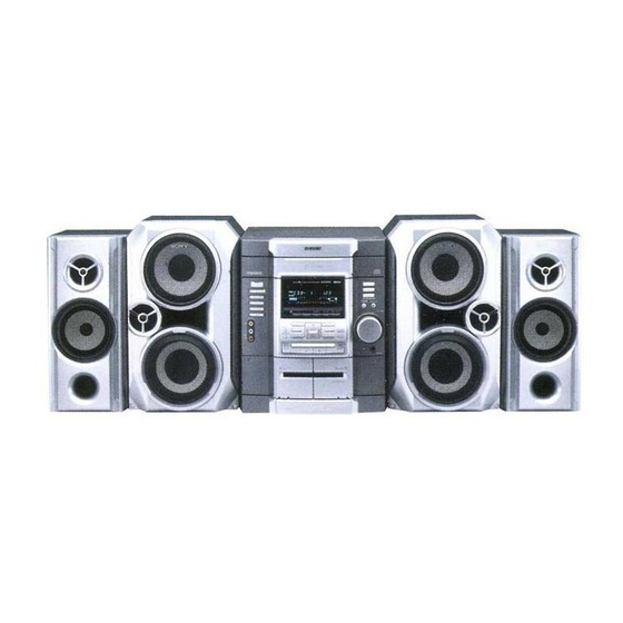
• HCD-RG66 is the tuner, deck, CD and
amplifier section in MHC-RG66.
TE
L 13942296513
Amplifier section
AEP and UK models:
DIN power output (rated)
Continuous RMS power output (reference)
Music power output (reference)
Singapore and Australian models:
The following measured at AC 120, 220, 230 –
240 V, 50/60 Hz
DIN power output (rated) 115 + 115 watts (6 ohms
Continuous RMS power output (reference)
Inputs
MD/VIDEO (AUDIO) IN (phono jacks):
GAME (AUDIO) IN (phono jack):
MIC (phone jack) (except for European models):
Outputs
PHONES (stereo mini jack):
Front speaker:
Surround speaker:
www
.
Sony Corporation
9-873-972-01
Home Audio Company
2002D1600-1
Published by Sony Engineering Corporation
© 2002.04
http://www.xiaoyu163.com
CD player section
System
115 + 115 watts (6 ohms
at 1 kHz, DIN)
Laser
140 + 140 watts (6 ohms
at 1 kHz, 10% THD)
Frequency response
280 + 280 watts (6 ohms
Wavelength
at 1 kHz, 10% THD)
Signal-to-noise ratio
Dynamic range
CD OPTICAL DIGITAL OUT
(Square optical connector jack, rear panel)
Wavelength
Output Level
at 1 kHz, DIN)
Tape deck section
Recording system
140 + 140 watts (6 ohms
Frequency response
at 1 kHz, 10% THD)
voltage 450/250 mV,
Tuner section
impedance 47 kilohms
FM stereo, FM/AM superheterodyne tuner
FM tuner section
voltage 450 mV,
Tuning range 87.5 – 108.0 MHz
impedance 47 kilohms
Antenna FM lead antenna
Antenna terminals 75 ohm unbalanced
sensitivity 1 mV,
Intermediate frequency 10.7 MHz
impedance 10 kilohms
AM tuner section
Tuning range
accepts headphones of
European and Middle Eastern models:
8 ohms or more
accepts impedance of 6 to
16 ohms
accepts impedance of
24 ohms
x
ao
u163
y
i
http://www.xiaoyu163.com
HCD-RG66
2 9
8
Model Name Using Similar Mechanism
CD
CD Mechanism Type
Section
Optical Pick-up Name
Tape deck
Model Name Using Similar Mechanism
Section
Tape Transport Mechanism Type
Q Q
3
6 7
1 3
1 5
SPECIFICATIONS
Compact disc and digital
audio system
Semiconductor laser
(λ =780 nm)
Emission duration:
continuous
2 Hz – 20 kHz (±0.5 dB)
780 – 790 nm
More than 90 dB
More than 90 dB
660 nm
–18 dBm
4-track 2-channel stereo
50 – 13,000 Hz (±3 dB),
using Sony TYPE I
cassette
531 – 1,602 kHz (with the
interval set at 9 kHz)
MINI HI-FI COMPONENT SYSTEM
co
.
9 4
2 8
AEP Model
UK Model
E Model
Australian model
NEW
CDM58F-K6A
KSM-213DCP
NEW
CWL43RR-51
0 5
8
2 9
9 4
2 8
Other models:
531 – 1,602 kHz (with the
interval set at 9 kHz)
530 – 1,710 kHz (with the
interval set at 10 kHz)
Antenna
AM loop antenna
Antenna terminals
External antenna terminal
Intermediate frequency
450 kHz
General
Power requirements
AEP and UK models:
230 V AC, 50/60 Hz
Australian model:
230 – 240 V AC, 50/
60 Hz
Singapore model:
120 V, 220 V or 230 –
240 V AC, 50/60 Hz
Adjustable with voltage
selector
Power consumption
AEP and UK models:
220 watts
0.5 watts (at the Power
Saving Mode)
Singapore and Australian models:
220 watts
Approx. 280 × 325 × 421 mm
Dimensions (w/h/d)
Mass
Approx. 10.5 kg
Supplied accessories:
AM loop antenna (1)
Remote Commander (1)
Batteries (2)
FM lead antenna (1)
Front speaker pads (8)
Design and specifications are subject to change
without notice.
m
9 9
9 9
Advertisement
Table of Contents

Related Manuals for Sony HCD-RG66


Summary of Contents for Sony HCD-RG66
- Page 1 3 7 63 1515 0 SERVICE MANUAL AEP Model UK Model Ver 1.0 2002. 04 E Model Australian model • HCD-RG66 is the tuner, deck, CD and amplifier section in MHC-RG66. Model Name Using Similar Mechanism CD Mechanism Type CDM58F-K6A Section Optical Pick-up Name...
-
Page 2: Table Of Contents
MARK 0 ON THE SCHEMATIC DIAGRAMS AND IN THE PARTS LIST ARE CRITICAL TO SAFE OPERATION. REPLACE THESE 6-4. CD Mechanism Deck Section (CDM58F-K6A) ········· 43 COMPONENTS WITH SONY PARTS WHOSE PART NUMBERS APPEAR AS SHOWN IN THIS MANUAL OR IN SUPPLEMENTS 7. ELECTRICAL PARTS LIST ·······································... -
Page 3: General
HCD-RG66 SECTION 1 GENERAL 3 7 63 1515 0 This section is extracted from instruction manual. Main unit ALPHABETICAL ORDER BUTTON DESCRIPTIONS A – G M – Z ?/1 (power) 1 v/V/b/B 5 MD (VIDEO) wl (30) AUDIO jacks wh (29) - Page 4 HCD-RG66 3 7 63 1515 0 Remote Control ALPHABETICAL ORDER BUTTON DESCRIPTIONS ?/1 (power) 4 A – G M – Z CD qj (12, 13, 19, 20) MD (VIDEO) 9 (30) CLEAR 6 (13) P FILE qd (23) CLOCK/TIMER SELECT 2 PRESET +/–...
-
Page 5: Disassembly
HCD-RG66 SECTION 2 DISASSEMBLY 3 7 63 1515 0 Note : Disassemble the unit in the order as shown below. CASE (TOP) CD DOOR FRONT PANEL SECTION CD MECHANISM DECK (CDM58F-K6A) MIC BOARD, PANEL BOARD, TAPE MECHANISM DECK (CWL43RR-51) -
Page 6: Cd Door
HCD-RG66 3 7 63 1515 0 2-2. CD Door 4 CD door CD mechanism deck (CDM58F-K6A) 1 Turn the pulley to the direction of arrow. Front panel side pulley 2 Pull-out the disc tray. L 13942296513 2-3. Front Panel Section 6 connector 2p (CN605) 4 screw (+BVTP 3 ×... -
Page 7: Cd Mechanism Deck (Cdm58F-K6A)
HCD-RG66 3 7 63 1515 0 2-4. CD Mechanism Deck (CDM58F-K6A) 3 CD mechanism deck (CDM58F-K6A) 1 connector 8p (CN734) L 13942296513 2-5. Tape Mechanism Deck (CWL43RR-51) 2 three ground wires 1 six screws (+PTPWH M2.6) 3 tape mechanism deck... -
Page 8: Mic Board, Panel Board, Rem Board
HCD-RG66 3 7 63 1515 0 2-6. MIC Board, PANEL Board, REM Board two claws two claws REM board claw 7 eleven screws q; REM board (+PTPWH M2.6) three claws 5 connector 3p (CN663) 9 connector 7p (CN661) 1 volume knob... -
Page 9: Back Panel Section
HCD-RG66 3 7 63 1515 0 2-8. Back Panel Section qa back panel 5 connector (CN2) 4 screw ( +BVTP 3 × 10) 2 three screws (+BVTP 3 × 10) 8 connector 2p (CN504) (from POWER board) 3 screw (+BVTP 3 ×... -
Page 10: Main Board
HCD-RG66 3 7 63 1515 0 2-10. MAIN Board 4 MAIN board 1 two screws (+BVTT 3 × 6) 3 connector 13p (CN502) MAIN board L 13942296513 2 connector 13p (CN503) 2-11. POWER Board 5 two screws (+BVTT 3 × 6) 2 three screws (+BVTT 3 ×... -
Page 11: Trans Board
HCD-RG66 3 7 63 1515 0 2-12. TRANS Board 2 two screws (+BVTT 4× 6) 1 two screws (+BVTT 4× 6) 3 TRANS board L 13942296513 2-13. BD Board, DRIVER Board 3 connector 6p (CN732) 4 four screws (+BTTP M2.6 ) -
Page 12: Spdl Mortr Board
HCD-RG66 3 7 63 1515 0 2-14. SPDL MORTR Board 1 Remove solders. (four places) 2 Remove solders. (four places) 3 SPDL MOTOR board L 13942296513 2-15. Optical Pick-up (KSM-213DCP) 3 screw (+PTPWH M2.6) 4 holder (BU) assy q; screw (DIA. 12) -
Page 13: Motor Board, Address Sensor Board
HCD-RG66 3 7 63 1515 0 2-16. MOTOR Board, ADDRESS SENSOR Board 3 screw (+PTPWH 2.6 × 8) 4 tray 6 two screws (+BTTP M2.6) 8 MOTOR board 7 Remove the two solderings of motor. 9 screw (+BTTP M2.6) -
Page 14: Test Mode
HCD-RG66 SECTION 3 TEST MODE 3 7 63 1515 0 [Cold Reset] Aging mode in Tape Deck section • The cold reset clears all data including preset data stored in the 1) Operation during aging mode RAM to initial conditions. Execute this mode when returning •... - Page 15 HCD-RG66 3 7 63 1515 0 [Version and Destination Display Mode] • The version or destination is displayed. Procedure: 1. Press the ?/1 button to turn the set ON. 2. To enter the test mode, press the three buttons x , GAME EQ and MOVIE EQ simultaneously.
-
Page 16: Electrical Adjustments
HCD-RG66 SECTION 4 ELECTRICAL ADJUSTMENTS 3 7 63 1515 0 AM IF Adjustment TUNER SECTION FM Tuned Level Adjustment AM RF Signal generator FM RF Signal generator 75 Ω coaxial 30% amplitude Carrier frequency : 98 MHz modulation by... - Page 17 HCD-RG66 3 7 63 1515 0 CD SECTION Note : 1. CD Block is basically designed to operate without adjustment. Therefore, check each item in order given. 2. Use YEDS-18 disc (3-702-101-01) unless otherwise indicated. 3. Use an oscilloscope with more than 10MΩ impedance.
-
Page 18: Diagrams
HCD-RG66 SECTION 5 DIAGRAMS 3 7 63 1515 0 THIS NOTE IS COMMON FOR PRINTED WIRING BOARDS AND SCHEMATIC DIAGRAMS. (In addition to this, the necessary note is printed in each block.) Note on Schematic Diagram: Note on Printed Wiring Boards: •... -
Page 19: Circuit Boards Location
HCD-RG66 3 7 6 3 1 5 1 5 0 5-1. Circuit Boards Location • Waveforms IC751 rf (XOUT) IC102 ws (XOUT) SUB TRANS board 5.0 Vp-p 5.6 Vp-p 59 ns 222 ns BD board 2 V/DIV, 20 ns/DIV... -
Page 20: Block Diagrams -Tuner Section
HCD-RG66 5-2. Block Diagrams –TUNER Section– 3 7 6 3 1 5 1 5 0 EXCEPT AEP,UK IC101 JK101 FE101 Q101 AM/FM IF MPX CF101 CF102 RF IF L-CH ANT IN IF OUT FM IF L OUT FM 75Ω... -
Page 21: Main Section
HCD-RG66 MAIN Section 3 7 6 3 1 5 1 5 0 R CH JK801 PHONES IC501 Q363 IC301 POWER AMP MUTE SOUND PROCESSOR L-CH IN2B OUT2 SECTION Q301 RY371 MUTE CD-L Q631 JK302 Q381,382 Q383 Q386 Q384,385 IN2A... -
Page 22: Printed Wiring Boards - Cd Section (1/2)
HCD-RG66 5-3. Printed Wiring Boards – CD Section (1/2) – • See page 19 for Circuit Boards Location. 3 7 6 3 1 5 1 5 0 DRIVER BOARD BD BOARD CN701 (Page 23) • Semiconductor Location Ref. No. Location... -
Page 23: Printed Wiring Boards - Cd Section (2/2)
HCD-RG66 5-4. Printed Wiring Boards – CD Section (2/2) – • See page 19 for Circuit Boards Location. 3 7 6 3 1 5 1 5 0 C712 1 3 9 4 2 2 9 6 5 1 3... -
Page 24: Schematic Diagram - Cd Section
HCD-RG66 5-5. Schematic Diagram – CD Section – • See page 35 for IC Block Diagrams. • See page 19 for Waveforms. 3 7 6 3 1 5 1 5 0 BD BOARD OPTICAL PICK-UP CN733 BLOCK (KSM-213DCP) 0.022 LED DRIVER 0.022... -
Page 25: Printed Wiring Board - Main Section
HCD-RG66 5-6. Printed Wiring Board – MAIN Section – • See page 19 for Circuit Boards Location. 3 7 6 3 1 5 1 5 0 • Semiconductor Location Ref. No. Location PANEL MAIN BOARD BD BOARD BOARD CN734... -
Page 26: Schematic Diagram - Main Section (1/4)
HCD-RG66 5-7. Schematic Diagram – MAIN Section (1/4) – • See page 36, 37 for IC Block Diagrams. • See page 19 for Waveforms. 3 7 6 3 1 5 1 5 0 (1/4) MAIN BOARD AEP,UK SP,AUS +B SWITCH 11.9... -
Page 27: Schematic Diagram - Main Section (2/4)
HCD-RG66 5-8. Schematic Diagram – MAIN Section (2/4) – • See page 19 for Waveforms. 3 7 6 3 1 5 1 5 0 (2/4) MAIN BOARD 4..7k 0.47 0.01 TAPE DECK 0.0022 (1/2) 0.01 0.001 DECK A Q210,211 0.001... -
Page 28: Schematic Diagram - Main Section (3/4)
HCD-RG66 5-9. Schematic Diagram – MAIN Section (3/4) – • See page 36 for IC Block Diagrams. 3 7 6 3 1 5 1 5 0 MAIN BOARD (1/4) MAIN BOARD (Page 26) (2/4) (Page 27) 7 8 9 10... -
Page 29: Schematic Diagram - Main Section (4/4)
HCD-RG66 5-10. Schematic Diagram – MAIN Section (4/4) – 3 7 6 3 1 5 1 5 0 MAIN BOARD (2/4) (Page 27) 52 53 54 (4/4) MAIN BOARD PANEL BOARD 0.022 CN801 (Page 31) IC304 NJM4565M <4.6> IC304... -
Page 30: Printed Wiring Boards - Panel Section
HCD-RG66 5-11. Printed Wiring Boards – PANEL Section – • See page 19 for Circuit Boards Location. 3 7 6 3 1 5 1 5 0 PANEL BOARD BOARD CN733 (Page 22) DISK 1 DISK 2 AEP,UK DISK 3... -
Page 31: Schematic Diagram - Panel Section
HCD-RG66 5-12. Schematic Diagram – PANEL Section – • See page 38 for IC Pin Function Description. • See page 19 for Waveforms. 3 7 6 3 1 5 1 5 0 BD BOARD CN733 (Page 24) CN804 PANEL BOARD FLD801 0.033... -
Page 32: Printed Wiring Boards - Power/Trans Section
HCD-RG66 5-13. Printed Wiring Boards – POWER/TRANS Section – • See page 19 for Circuit Boards Location. 3 7 6 3 1 5 1 5 0 POWER AMP BOARD TRANS BOARD IC501 120V 220V 230-240V AEP,UK AEP,UK VOLTAGE SELECTOR... -
Page 33: Schematic Diagram - Power/Trans Section
HCD-RG66 5-14. Schematic Diagram – POWER/TRANS Section – 3 7 6 3 1 5 1 5 0 TRANS BOARD POWER AMP BOARD POWER TRANSFORMER SP,AUS IC501 230-240V (1/2) 52.4 220V AEP,UK,SP POWER AMP 53.8 Q501,551 -0.1 OVER LOAD DETECT AEP,UK T6.3AL/250V... -
Page 34: Printed Wiring Board - Surround/Keyboard Section
HCD-RG66 3 7 6 3 1 5 1 5 0 5-15. Printed Wiring Board – SURROUND/KEYBOARD Section – 5-16. Schematic Diagram – SURROUND/KEYBOARD Section – KEYBOARD BOARD PANEL BOARD CN661 (Page 30) SURROUND BOARD S813 SURROUND MOVIE EQ SPEAKER MODE... - Page 35 HCD-RG66 3 7 63 1515 0 • IC Block Diagrams IC731 LA9242M (BD BOARD) 58 57 55 54 53 52 51 50 RF DET FIN2 FINI I / V DGND ∝-COM INTERFACE RFS- RFSM RF AMP TESI T. SERVO & T. LOGIC...
- Page 36 HCD-RG66 3 7 63 1515 0 IC781 BA6898FP (BD BOARD) LEVEL SHIFT LEVEL SHIFT THERMAL SHUT DOWN DRIVER MUTE REG VOLTAGE DOWN, BIAS VOLTAGE DOWN, THERMAL SHUT DOWN MONITOR LEVEL SHIFT LEVEL SHIFT L 13942296513 IC101 LA1845 (MAIN BOARD) PF.AMP...
- Page 37 HCD-RG66 3 7 63 1515 0 IC301 M61519FPD61G (MAIN BOARD) IC102 LC72131D (MAIN BOARD) L 13942296513 PHASE DETECTOR CHARGE PUMP POWER REFERENCE UNLOCK DIVIDER DETECTOR RESET SWALLOW COUNTER 1/16, 1/17 4BITS 12BITS PROGRAMMABLE DRIVER UNIVERSAL DATA SHIFT REGISTER LATCH...
-
Page 38: Ic Pin Function Description
HCD-RG66 3 7 63 1515 0 5-17. IC PIN FUNCTION DESCRIPTION • IC801 LC876662B-5Z81 Master Control (PANEL Board) Pin No. Pin Name Description PWR LED PWR LED control signal output P.S.RELAY Standby relay control signal output SYS MUTE System muting signal output... - Page 39 HCD-RG66 3 7 63 1515 0 Pin No. Pin Name Description CD U/D SW CD BU up/down switch signal input STEREO Stereo tuning signal input TUNED Tuning a frequency signal input TAPE PHOTO A deck photo sensor singanl input...
-
Page 40: Exploded Views
HCD-RG66 SECTION 6 EXPLODED VIEWS 3 7 63 1515 0 NOTE: • -XX, -X mean standardized parts, so they may • The mechanical parts with no reference number • Abbreviation have some differences from the original one. in the exploded views are not supplied. -
Page 41: Front Panel Section
HCD-RG66 3 7 63 1515 0 6-2. Front Panel Section not supplied FLD801 not supplied L 13942296513 supplied Ref. No. Part No. Description Remarks Ref. No. Part No. Description Remarks X-4954-709-1 PANEL ASSY, FRONT (AUS, SP) 4-238-647-01 FL HOLDER L... -
Page 42: Main Board Section
HCD-RG66 3 7 63 1515 0 6-3. MAIN Board Section F919 T911 F920 F914 not supplied L 13942296513 not supplied Ref. No. Part No. Description Remarks Ref. No. Part No. Description Remarks 1-751-688-11 WIRE (FLAT TYPE) (13 CORE) A-4729-636-A POWER BOARD, COMPLETE (AEP, UK) -
Page 43: Cd Mechanism Deck Section (Cdm58F-K6A)
HCD-RG66 3 7 63 1515 0 6-4. CD Mechanism Deck Section (CDM58F-K6A) supplied M721 supplied supplied supplied L 13942296513 supplied supplied Ref. No. Part No. Description Remarks Ref. No. Part No. Description Remarks 4-218-254-21 SCREW (M2.6), +PTPWH 4-985-672-01 SCREW (+PTPWH M2.6), FLOATING... -
Page 44: Electrical Parts List
HCD-RG66 SECTION 7 ADDRESS SENSOR ELECTRICAL PARTS LIST 3 7 63 1515 0 NOTE: • Due to standardization, replacements in the • CAPACITORS: • COILS uF: µF uH: µH parts list may be different from the parts specified in the diagrams or the components •... - Page 45 HCD-RG66 3 7 63 1515 0 Ref. No. Part No. Description Remarks Ref. No. Part No. Description Remarks C787 1-104-665-11 ELECT 100uF 20.00% 10V R725 1-249-430-11 CARBON 1/4W C788 1-162-290-31 CERAMIC 470PF R727 1-249-430-11 CARBON 1/4W C789 1-164-159-21 CERAMIC 0.1uF...
- Page 46 HCD-RG66 DRIVER KEYBOARD MAIN 3 7 63 1515 0 Ref. No. Part No. Description Remarks Ref. No. Part No. Description Remarks R793 1-247-807-31 CARBON 1/4W R821 1-216-835-11 METAL CHIP 1/16W R794 1-249-437-11 CARBON 1/4W R822 1-216-837-11 METAL CHIP 1/16W...
- Page 47 HCD-RG66 MAIN 3 7 63 1515 0 Ref. No. Part No. Description Remarks Ref. No. Part No. Description Remarks C112 1-162-970-11 CERAMIC CHIP 0.01uF C179 1-162-970-11 CERAMIC CHIP 0.01uF C113 1-126-959-11 ELECT 0.47uF 20.00% 50V (AEP, UK) C114 1-126-947-11 ELECT 47uF 20.00% 16V...
- Page 48 HCD-RG66 MAIN 3 7 63 1515 0 Ref. No. Part No. Description Remarks Ref. No. Part No. Description Remarks C285 1-162-966-11 CERAMIC CHIP 0.0022uF 10% C382 1-126-961-11 ELECT 2.2uF 20.00% 50V C286 1-162-966-11 CERAMIC CHIP 0.0022uF 10% C383 1-126-961-11 ELECT 2.2uF...
- Page 49 HCD-RG66 MAIN 3 7 63 1515 0 Ref. No. Part No. Description Remarks Ref. No. Part No. Description Remarks D602 8-719-988-61 DIODE 1SS355TE-17 JR118 1-216-864-11 METAL CHIP 1/16W D681 8-719-083-89 DIODE 11ES2N-TB5 JR120 1-216-864-11 METAL CHIP 1/16W D682 8-719-083-89 DIODE 11ES2N-TB5...
- Page 50 HCD-RG66 MAIN 3 7 63 1515 0 Ref. No. Part No. Description Remarks Ref. No. Part No. Description Remarks Q381 8-729-119-78 TRANSISTOR 2SC2785TP-HFE R130 1-216-827-11 METAL CHIP 3.3K 1/16W Q382 8-729-119-78 TRANSISTOR 2SC2785TP-HFE (AEP, UK) Q383 8-729-119-76 TRANSISTOR 2SA1175TP-HFE...
- Page 51 HCD-RG66 MAIN 3 7 63 1515 0 Ref. No. Part No. Description Remarks Ref. No. Part No. Description Remarks R231 1-216-825-11 METAL CHIP 2.2K 1/16W R327 1-216-829-11 METAL CHIP 4.7K 1/16W R232 1-216-825-11 METAL CHIP 2.2K 1/16W (AUS, SP)
- Page 52 HCD-RG66 MAIN MOTOR PANEL 3 7 63 1515 0 Ref. No. Part No. Description Remarks Ref. No. Part No. Description Remarks R607 1-216-832-11 METAL CHIP 8.2K 1/16W < SWITCH > R608 1-216-832-11 METAL CHIP 8.2K 1/16W R609 1-216-844-11 METAL CHIP...
- Page 53 HCD-RG66 PANEL 3 7 63 1515 0 Ref. No. Part No. Description Remarks Ref. No. Part No. Description Remarks C837 1-162-294-31 CERAMIC 0.001uF D823 8-719-991-33 DIODE 1SS133T-77 C838 1-104-665-11 ELECT 100uF 20.00% 10V D824 8-719-991-33 DIODE 1SS133T-77 (AUS, SP)
- Page 54 HCD-RG66 PANEL 3 7 63 1515 0 Ref. No. Part No. Description Remarks Ref. No. Part No. Description Remarks R690 1-247-807-31 CARBON 1/4W R877 1-247-891-00 CARBON 330K 1/4W R801 1-249-410-11 CARBON 1/4W F R878 1-249-417-11 CARBON 1/4W F R879...
- Page 55 HCD-RG66 POWER 3 7 63 1515 0 Ref. No. Ref. No. Part No. Part No. Description Description Remarks Remarks Ref. No. Part No. Description Remarks A-4676-523-A POWER BOARD, COMPLETE (AUS, SP) Q582 8-729-140-84 TRANSISTOR 2SC1841TP-PAFAEA A-4729-636-A POWER BOARD, COMPLETE (AEP, UK)
- Page 56 HCD-RG66 SENSOR SPDL MOTOR SUB TRANS SURROUND TRANS 3 7 63 1515 0 Ref. No. Part No. Description Remarks Ref. No. Part No. Description Remarks 1-684-558-11 SENSOR BOARD 1-684-494-11 SURROUND BOARD ************** **************** < THERMISTOR > < CONNECTOR >...
- Page 57 HCD-RG66 VIDEO OUT 3 7 63 1515 0 Ref. No. Part No. Description Remarks Ref. No. Part No. Description Remarks 1-684-556-11 VIDEO OUT BOARD **************** < JACK > JK602 1-774-227-31 JACK, PIN 1P(VIDEO OUT) ************************************************************** MISCELLANEOUS ************** 1-763-072-11 FAN, DC (AEP,UK)
- Page 58 HCD-RG66 3 7 63 1515 0 REVISION HISTORY Clicking the version allows you to jump to the revised page. Also, clicking the version at the upper right on the revised page allows you to jump to the next revised page.