Table of Contents
Advertisement
Specifications
lGENERAL
Power Supply:
Power Consumption:
Power Consumption in Standby Mode:
Dimensions (W×H×D):
Mass:
Operating Temperature Range:
Operating Humidity Range:
lAMPLIFIER SECTION
RMS Output Power: Dolby Digital Mode
lTotal RMS Dolby Digital mode power:
At 1 kHz and total harmonic of 10%
lFront Ch:
lCenter Ch:
lSurround Ch:
AC 110 to 127 V, 220 to 240
V, 50/60 Hz
135 W
approx. 0.8 W
430×60×363 mm
Main unit approx. 3.5 kg
+5°C to +35°C
5% to 90% RH (no
condensation)
750 W
125 W / Channel (3 Ω)
125 W / Channel (3 Ω)
125 W / Channel (3 Ω)
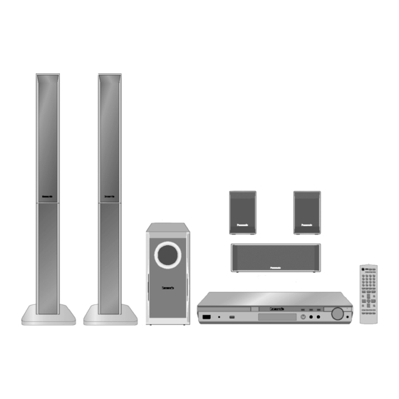
DVD Home Theater Sound System
SA-PT250GCP
Colour
(S).......................Silver Type
At 100 Hz and total harmonic of 10%
lSubwoofer Ch:
PMPO Output Power:
DIN Output Power: Dolby Digital Mode
lTotal DIN Dolby Digital mode power:
At 1 kHz and total harmonic of 1%
lFront Ch:
lCenter Ch:
lSurround Ch:
At 100 Hz and total harmonic of 1%
lSubwoofer Ch:
lFM TUNER, TERMINALS SECTION
Preset Memory:
Frequency Modulation (FM)
Frequency range:
Sensitivity:
S/N 26 dB:
© 2007 Matsushita Electric Industrial Co., Ltd. All
rights
reserved.
distribution is a violation of law.
ORDER NO. MD0705013CE
125 W / Channel (3 Ω)
5600 W
450 W
75 W / Channel (3 Ω)
75 W / Channel (3 Ω)
75 W / Channel (3 Ω)
75 W / Channel (3 Ω)
FM 30 stations
87.50-108.00 MHz
(50-kHz step)
1.8 µV (IHF)
1.4 µV
Unauthorized
copying
and
Advertisement
Table of Contents

Related Manuals for Panasonic SA-PT250GCP


Summary of Contents for Panasonic SA-PT250GCP
-
Page 1: Specifications
ORDER NO. MD0705013CE DVD Home Theater Sound System SA-PT250GCP Colour (S).......Silver Type Specifications lGENERAL At 100 Hz and total harmonic of 10% 125 W / Channel (3 Ω) Power Supply: AC 110 to 127 V, 220 to 240 lSubwoofer Ch:... - Page 2 160 x 120 and 6144 x 4096 pixels (Sub sampling is 4:0:0, 4:2:0, 4:2:2, or 4:4:4). Extremely long and narrow pictures may not be displayed. *5 MPEG4 data recorded with the Panasonic SD multi cameras or DVD video recorders. lConforming to SD VIDEO specifications (ASF standard)/ MPEG4 (Simple Profile) video system/G.726 audio system.
- Page 3 SA-PT250GCP CONTENTS Page Page 1 Safety Precautions 1.3. Protection Circuitry 1.1. GENERAL GUIDELINES 1.4. Safety Parts Information 1.2. Before Repair and Adjustment...
-
Page 4: Table Of Contents
SA-PT250GCP 2 Prevention of Electrostatic Discharge (ESD) to 11.5. Checking & Repairing DVD Module P.C.B. Electrostatically Sensitive (ES) Devices 11.6. Checking & Repairing SMPS P.C.B. 3 Precaution of Laser Diode 12 Measurements and Adjustments 4 About Lead Free Solder (PbF) 12.1. - Page 5 SA-PT250GCP 25 Replacement Parts List 25.1. Component Parts List...
-
Page 6: Before Repair And Adjustment
SA-PT250GCP 1 Safety Precautions 1.1. GENERAL GUIDELINES 1. When servicing, observe the original lead dress. If a short circuit is found, replace all parts which have been overheated or damaged by the short circuit. 2. After servicing, see to it that all the protective devices such as insulation barriers, insulation papers shields are properly installed. -
Page 7: Safety Parts Information
SA-PT250GCP “shorted”, or if speaker systems with an impedance less than the indicated rated impedance of the amplifier are used. If this occurs, follow the procedure outlines below: 1. Turn off the power. 2. Determine the cause of the problem and correct it. -
Page 8: Electrostatically Sensitive (Es) Devices
SA-PT250GCP 2 Prevention of Electrostatic Discharge (ESD) to Electrostatically Sensitive (ES) Devices Some semiconductor (solid state) devices can be damaged easily by static electricity. Such components commonly are called Electrostatically Sensitive (ES) Devices. Examples of typical ES devices are integrated circuits and some field-effect transistors and semiconductor "chip"... -
Page 9: Precaution Of Laser Diode
SA-PT250GCP 3 Precaution of Laser Diode CAUTION : This product utilizes a laser diode with the unit turned on, invisible laser radiation is emitted from the pickup lens. Wavelength : 662nm/785nm Maximum output radiation power from pickup : 100µW/VDE Laser radiation from pickup unit is safety level, but be sure the followings: 1. -
Page 10: About Lead Free Solder (Pbf)
SA-PT250GCP 4 About Lead Free Solder (PbF) 4.1. Service caution based on legal restrictions 4.1.1. General description about Lead Free Solder (PbF) The lead free solder has been used in the mounting process of all electrical components on the printed circuit boards used for this equipment in considering the globally environmental conservation. -
Page 11: Handling Precautions For Traverse Unit
SA-PT250GCP 5 Handling Precautions for Traverse Unit The laser diode in the optical pickup unit may break down due to static electricity of clothes or human body. Special care must be taken avoid caution to electrostatic breakdown when servicing and handling the laser diode in the traverse unit. - Page 12 SA-PT250GCP...
-
Page 13: Accessories
SA-PT250GCP 6 Accessories · Note: Refer to “Replacement Parts List” (Section 25) for the part number. Screw Remote control Speaker cord Antenna wire Speaker label AC cord Video cable AC plug adaptor... -
Page 14: Operation Procedures
SA-PT250GCP 7 Operation Procedures 7.1. Remote Control Key Buttons Operations Television operations Adjust the television volume Select the source DVD/CD EXT-IN: USB , AUX , MUSIC P. Switch the main unit on or off Change the television’s video input mode Select disc’s title numbers and etc.,... -
Page 15: Main Unit Key Buttons Operations
SA-PT250GCP 7.2. Main Unit Key Buttons Operations /MEMORY Disc playback , Memorise the receiving radio stations Standby/on switch [ /I] Press to switch the unit from on to / TUNE MODE / FM MODE standby mode or vice versa. In standby... -
Page 16: Music Port Connection And Operation
SA-PT250GCP 7.3. Music Port Connection and Operation The Music Port allows you to connect and enjoy music from To select "MUSIC P.". an external device (example: MP3 player) through your home theater system. MUSIC P. Preparation To avoid distorted sound, make sure that any equalizer function of your external device is turned off. -
Page 17: Usb Connection And Operation
Music .mp3 port USB card reader. Typically the fi rst memory card inserted. .wma Video .asf MPEG4 It may not be possible to play all the fi les due to the condition on how they were created. For Panasonic D-Snap/DIGA. -
Page 18: Optional Audio Connection For Video Cassette Recorder Or Television
SA-PT250GCP 7.5. Audio & Video Connections 7.5.1. Optional Connection for Set Top Box, Cable TV, or Video Cassette Recorder To your cable TV service or television antenna RF cable (not included) Audio cable (not included) Television Rear panel of (not included) -
Page 19: Disc Information
Closing the session will also work. MPEG4 data recorded with the Panasonic SD multi cameras or DVD video recorders [conforming to SD VIDEO specifi cations (ASF standard)/MPEG4 (Simple Profi le) video system/G.726 audio system]. - Page 20 You can play MPEG4 data [conforming to SD VIDEO specifi cations (ASF standard)/MPEG4 (Simple Profi le) video system/G.726 audio system] recorded with Panasonic SD multi cameras or DVD video rec orders with this unit. The recording date may differ from that of the actual date.
-
Page 21: Self-Diagnosis And Special Mode Setting
SA-PT250GCP 8 Self-Diagnosis and Special Mode Setting 8.1. Service Mode Summary Table The service modes can be activated by pressing various button combination on the main unit and remote control unit. Below is the summary for the various modes for checking:... -
Page 22: Service Mode Table
SA-PT250GCP 8.2.1. Service Mode Table 1 Item Key Operation FL Display Mode Name Description Front Key Jitter check Jitter check. In STOP (no disc) mode, (Display 1) Jitter rate is measured and displayed. press [STOP] button on the Measurement is repeatedly done in main unit, and [5] button on the cycle of one second. - Page 23 SA-PT250GCP 8.2.2. Service Mode Table 2 Key Operation Item FL Display Mode Name Description Front Key (Display 1) DVD laser DVD laser drive current measurement. In STOP (no disc) mode, drive current DVD laser drive current is measured press [STOP] button on the...
- Page 24 SA-PT250GCP 8.2.3. Service Mode Table 3 Item Key Operation FL Display Mode Name Description Front Key Micro-processor Micro-processor firmware version In STOP (no disc) (Display 1) firmware version display & EEPROM checksum display. mode, press [STOP] display & EEPROM checksum is only available...
- Page 25 SA-PT250GCP Product Region TV Broadcasting Model Series Country Region Signal System Region Display Code OSD Menu Language System (Default) (Default) English, Spanish, Canadian P, PC, PX USA, Canada, PX NTSC NTSC (*A) French Japan NTSC NTSC (*A) Japanese, English English, French, German,...
- Page 26 SA-PT250GCP 8.2.4. Service Mode Table 4 Item Key Operation FL Display Mode Name Description Front Key DVD Module P.C.B. firmware version In STOP (no disc) Module P.C.B. is displayed on the FL Display. mode, press [STOP] firmware The firmware version can be updated...
- Page 27 SA-PT250GCP 8.2.5. Service Mode Table 5 Item Key Operation FL Display Mode Name Description Front Key Timer 1 check Timer 1 check In STOP (no disc) (Display 1) Laser operation timer is measured mode, press [STOP] separately for DVD laser and CD laser.
- Page 28 SA-PT250GCP 8.2.6. Optical Pick-up Self-Diagnosis The optical pickup self-diagnosis function and tilt adjustment check function have been included in this unit. When repairing, use the following procedure for effective self-diagnosis and tilt adjustment. Be sure to use the self-diagnosis function before replacing the optical pickup when "NO DISC"...
-
Page 29: Dvd Self Diagnostic Function-Error Code
SA-PT250GCP 8.3. DVD Self Diagnostic Function-Error Code 8.3.1. Mechanism Error Code Table Error Diagnosis Contents Description of error Automatic FL Display Remarks Code H01 Tray loading error The tray opening and closing is Press [ STOP] on abnormal. CLOSE and OPEN of the main unit for next error. - Page 30 SA-PT250GCP 8.3.2. DVD Module Error Code Table Error Diagnosis Contents Description of error Automatic FL Display Remarks Code U702 HDMI/DVI I2C The communication error of I2C Press [ STOP] on communication error when connecting it with HDMI/ main unit for next error.
- Page 31 SA-PT250GCP 8.3.3. Power Supply Error Code Table Error Diagnosis Contents Description of error Automatic FL Display Remarks Code F61 The abnormalities In normal operation, when DCDET2 Press [ STOP] on in an output or power goes to "L" (Low) (Not during POWER main unit for next error.
-
Page 32: Sales Demonstration Lock Function
SA-PT250GCP 8.3.5. USB Error Code Table Error Diagnosis Contents Description of error Automatic FL Display Remarks Code F650 USB device: Devices Devices other than the mass storage Press [ STOP] on other than mass class are connected. main unit for next error. -
Page 33: Service Precautions
SA-PT250GCP 8.5. Service Precautions 8.5.1. Recovery after the DVD player is repaired · When the FLASH ROM IC or DVD Module P.C.B. is replaced, carry out the recovery processing to optimize the drive. Playback the recovery disk to process the recovery automatically. -
Page 34: Assembling And Disassembling
SA-PT250GCP 9 Assembling and Disassembling “ATTENTION SERVICER” Be careful when disassembling and servicing. Some chassis components may have sharp edges. Special Note: 1. This section describes the disassembly procedures for all the major printed circuit boards and main components. 2. Before the disassembly process was carried out, do take special note that all safety precautions are to be carried out. -
Page 35: Disassembly Flow Chart
SA-PT250GCP 9.1. Disassembly Flow Chart 9.3. Top Cabinet 9.4. DVD Lid 9.10. Rear Panel 9.13. Main P .C.B. 9.14. Regulator IC 9.5. Front Panel (IC2903) 9.6. Volume P.C.B. 9.15. D-Amp P.C.B. 9.16. Digital Amp IC 9.7. Mic P.C.B. (IC5000) 9.8. Panel P.C.B. -
Page 36: Main Components And P.c.b. Locations
SA-PT250GCP 9.2. Main Components and P.C.B. Locations... -
Page 37: Disassembly Of Top Cabinet
SA-PT250GCP 9.3. Disassembly of Top Cabinet Step 1 Remove 4 screws. Step 2 Remove 3 screws at the rear panel Step 3 Lift up and remove the top cabinet in the direction of arrows. Step 2 Insert the gear jig into the tray open/ close hole. -
Page 38: Disassembly Of Front Panel
SA-PT250GCP Special Note : Avoid placing the set in a position that might cause damage to the jacks when removing the front panel. Note : You can return the tray by turning the gear jig clockwise. Step 4 Detach the front panel slightly forward in the direction of 9.5. -
Page 39: Disassembly Of Mic P.c.b
SA-PT250GCP 9.8. Disassembly of Panel P.C.B. · Disassembly of Earth Spring · Follow (Step 1) to (Step 3) of Item 9.3. Step 2 Remove 1 screw from the earth spring. · Follow (Step 1) to (Step 4) of Item 9.4. -
Page 40: Disassembly Of Usb P.c.b
SA-PT250GCP Step 3 Remove Voltage Selector P.B.C. from the catches at the rear panel. 9.9. Disassembly of USB P.C.B. · Follow (Step 1) to (Step 3) of Item 9.3. · Follow (Step 1) to (Step 4) of Item 9.4. · Follow (Step 1) to (Step 6) of Item 9.5. -
Page 41: Disassembly Of Dvd Module P.c.b
SA-PT250GCP Step 1 Remove 2 screws from the DVD mechanism unit. Step 2 Detach FFC cable from the connectors (CN2001) on Main P.C.B. and (CS901) on Tray Loading P.C.B. Step 2 Lift up DVD Module P.C.B. and detach FFC cable from the connector (FP8251). -
Page 42: Replacement Of Regulator Ic (Ic2903)
SA-PT250GCP Step 1 Detach FFC cable from the connectors (CN2007, 9.14. Replacement of Regulator IC CN2009, CN2013, CN2020 & CN9001) on Main P.C.B. and (IC2903) (CN5802) on SMPS P.C.B. Step 2 Remove the wire clamper to move aside the FFC cable ·... -
Page 43: Replacement Of Digital Amp Ic (Ic5000)
SA-PT250GCP Step 2 Remove the D-Amp P.C.B. bracket. Step 8 Remove Voltage Selector P.C.B. from the catches at the rear panel. · Disassembly of D-Amp P.C.B. Step 3 Remove the wire clamper to detach FFC cable from the connector (CN5801) on SMPS P.C.B. - Page 44 SA-PT250GCP Step 1 Desolder pins of the digital amp IC (IC5000) on the back Step 3 Remove the wire clamper to detach FFC cable from the side of D-Amp P.C.B. connector (CN5801) on SMPS P.C.B. Step 4 Detach FFC cable from the connector (CN5802) on SMPS P.C.B.
-
Page 45: Replacement Of Regulator Diode (D5801/D5802)
SA-PT250GCP Step 9 Remove SMPS, AC-Inlet & Voltage Selector P.C.B. Note : Refer to the diagrams of SMPS P.C.B. (Item 9.17) for location of the parts. 9.19. Replacement of Regulator Diode (D5801/D5802) · Follow (Step 1) to (Step 3) of Item 9.3. -
Page 46: Replacement Of Regulator Diode (D5803)
SA-PT250GCP Note : Refer to the diagrams of SMPS P.C.B. (Item 9.17) for location of the part. Note : Refer to the diagrams of SMPS P.C.B. (Item 9.17) for location of the parts. 9.20. Replacement of Regulator Diode (D5803) · Follow (Step 1) to (Step 3) of Item 9.3. -
Page 47: Assembly And Disassembly Of Dvd Mechanism Unit
SA-PT250GCP 10 Assembly and Disassembly of DVD Mechanism Unit 10.1. Disassembly Procedure Step 4 Remove the traverse unit. 10.1.1. Disassembly of Traverse Unit (with Middle Chassis) Step 1 Slide the lever (A) in the arrow direction (to the opposite side) till it stops. - Page 48 SA-PT250GCP l(Assembly of the tray unit) Step 2 Raise the mecha chassis vertically. Step 1 Insert a part of the tray into the unit sliding over the Step 3 Slide the lever in the arrow direction till it stops and pull groove on the mecha chassis.
- Page 49 SA-PT250GCP Step 4 Remove the belt. Step 5 Unlock the tab and remove the pulley gear. 10.1.3. Disassembly of Loading Section Step 6 Remove the relay gear. Step 1 Spread the tabs at the both sides and push out the drive arm.
-
Page 50: Disassembly Of Traverse Unit
SA-PT250GCP Step 9 Pull the lever (B) at the bottom side in the direction of arrow and remove the change lever. 10.1.5. Disassembly of Traverse Unit Step 1 Spread the tabs to push in the pin in the direction of arrows. - Page 51 SA-PT250GCP Step 3 Remove the middle chassis. Step 4 Remove the traverse unit.
-
Page 52: Service Position
SA-PT250GCP 11 Service Position 11.1. Checking & Repairing Panel P.C.B. Step 1 Remove the top cabinet. Step 2 Remove the DVD lid. Step 3 Disassemble the front panel. Step 4 Disassemble Panel P.C.B. Step 5 Disassemble Volume P.C.B. Step 6 Disassemble Mic P.C.B. -
Page 53: Module P.c.b
SA-PT250GCP Main P.C.B., (CN5050 & CN5501) on D-Amp P.C.B., (CN5801 11.5. Checking & Repairing DVD & CN5802) on SMPS P.C.B. (CS901) on Tray Loading P.C.B. Module P.C.B. and (FP9002) on USB P.C.B. · Follow (Step 1) to (Step 14) of Item 11.3. -
Page 54: Measurements And Adjustments
SA-PT250GCP 12 Measurements and Adjustments 12.1. Service Tools and Equipment Application Name Number Tilt adjustment DVD test disc DVDT-S20 [SPG] TORX screw driver (T6) Available on sales route. (T6) or RFKZ0185 [SPG] Others Grease RFKXPG641 [SPG] Confirmation CD test disc... -
Page 55: Optical Adjustment
SA-PT250GCP 12.4. Optical adjustment 12.4.1. Optical pickup tilt adjustment Measurement point Adjustment point Mode Disc Tangential adjustment screw T01 (inner periphery) play DVDT-S20 [SPG] Tilt adjustment screw T30 (center periphery) T43 (outer periphery) play Measuring equipment Adjustment value None (Main unit display for servicing is used.) Adjust to the minimum jitter value. - Page 56 SA-PT250GCP 13 Abbreviations INITIAL/LOGO ABBREVIATIONS ERROR TORQUE CONTROL ERROR TORQUE CONTROL INITIAL/LOGO ABBREVIATIONS REFERENCE A0~UP ADDRESS ENCSEL ENCODER SELECT ACLK AUDIO CLOCK ETMCLK EXTERNAL M CLOCK (81MHz/40.5MHz) AD0~UP ADDRESS BUS ETSCLK EXTERNAL S CLOCK (54MHz) ADATA AUDIO PES PACKET DATA...
- Page 57 SA-PT250GCP INITIAL/LOGO ABBREVIATIONS INITIAL/LOGO ABBREVIATIONS READ ENABLE VBLANK V BLANKING RFENV RF ENVELOPE COLLECTOR POWER SUPPLY RF PHASE DIFFERENCE OUTPUT VOLTAGE (CD-ROM) REGISTER SELECT VCDCONT VIDEO CD CONTROL (TRACKING RSEL RF POLARITY SELECT BALANCE) RESET DRAIN POWER SUPPLY VOLTAGE RESERVE...
-
Page 58: Dvd Module P.c.b
MODE CD PLAY IC9005 Ref No. MODE CD PLAY Q8321 Q8325 Q8331 Q8335 Q8341 Ref No. MODE CD PLAY Q8551 Q8552 Q8561 Q8562 Ref No. MODE CD PLAY QR8111 QR8420 QR8571 Ref No. MODE CD PLAY SA-PT250GCP DVD MODULE P.C.B. -
Page 59: Main P.c.b
-6.9 -10.9 -7.4 -7.4 -0.6 STANDBY 16.8 -0.6 -6.9 -7.5 -7.5 -0.6 Q2906 Q2907 Q2908 Q2909 Q2910 Ref No. MODE CD PLAY -2.5 STANDBY -2.4 Q2911 Q2916 Q2919 Q2921 Q2922 Ref No. MODE CD PLAY STANDBY 14.4 SA-PT250GCP MAIN P.C.B. -
Page 60: D-Amp P.c.b
Ref No. MODE CD PLAY STANDBY Q5604 Q5640 Q5641 Q5642 Q5644 Ref No. MODE CD PLAY 16.9 STANDBY 16.9 SA-PT250GCP D-AMP P.C.B. 14.4. SMPS P.C.B. IC5701 IC5799 IC5801 Ref No. MODE -14.6 -14.4 CD PLAY -11.3 -14.4 -14.6 -14.7 -14.6 -13.7... -
Page 61: Mic P.c.b
-22.2 Q6201 Ref No. MODE CD PLAY STANDBY SA-PT250GCP PANEL P.C.B. IC904 Ref No. MODE CD PLAY STANDBY SA-PT250GCP TRAY LOADING P.C.B. 14.6. Mic P.C.B. IC7000 Ref No. MODE CD PLAY -6.9 STANDBY -6.9 Ref No. IC7100 MODE CD PLAY... -
Page 62: Waveform Chart
SA-PT250GCP 14.7. Waveform Chart 14.7.1. Waveform 1 WF No. IC2001-15 (PLAY) WF No. IC2101-14,19 (PLAY) WF No. IC2101-15,16,17, 18 (PLAY) 5.2Vp-p(100nsec/div) 2.8Vp-p(100sec/div) 2.4Vp-p(200usec/div) 8Vp-p(200usec/div) WF No. IC2101-95, 96 (PLAY) 1.5Vp-p(200usec/div) 3.2Vp-p(200usec/div) 3.2Vp-p(200usec/div) 6.8Vp-p(200usec/div) WF No. IC2102- 7(PLAY) WF No. IC2801-4 (PLAY) WF No. - Page 63 SA-PT250GCP 14.7.2. Waveform 2 WF No. IC5400-2,22 (PLAY) WF No. IC5500-5 (PLAY) WF No. IC5500-8 (PLAY) WF No. IC5701-1,4 (PLAY) 0.6Vp-p(200usec/div) 7.2Vp-p(500nsec/div) 5.6Vp-p(500nsec/div) 170Vp-p(5msec/div) WF No. IC5799-2,3,5 (PLAY) WF No. IC5801-1,2,3 (PLAY) WF No. IC6901-5 (PLAY) 180Vp-p(5msec/div) 0.5Vp-p(2usec/div) 2.8Vp-p(100nsec/div)
-
Page 64: Illustration Of Ic's, Transistors And Diodes
SA-PT250GCP 15 Illustration of IC's, Transistors and Diodes C0ABBA000168 (8p) C0JBAF000716 (14p) C0HBB0000057 (44p) RFKWMH24B320 C0ABBB000230 (8p) C0JBAB000902 (14p) C1AB00002735 (100p) C0JBAB000908 (6p) C0ABBB000350 (8p) C2CBYY000440 (100p) C0CBCBD00018 (8p) C1BB00001061 (16p) MN2DS0018MP (216p) C0DBZYE00002 (8p) C3ABPG000145 (54p) No.1 C9ZB00000461 (32p) C0EBA0000029 (4p) No.1... -
Page 65: Wiring Connection Diagram
1 5 10 15 20 26 CN2009 FP8531 FP8251 FP9001 COMPONENT CN2007 VIDEO OUT FP8101 VIDEO OUT CN2013 MAIN P.C.B. JK2001 (SOLDER SIDE) CN2006 DVD MODULE P.C.B. DVD MODULE P.C.B. (SIDE:B) (SIDEA) CN2002 CN2001 CN2015 CN9002 CN9001 SA-PT250GCP WIRING CONNECTION... - Page 66 SA-PT250GCP...
-
Page 67: Block Diagram
FROM AUDIO HBASS SW HBASS SW CN2007 CN6902 KEY1 97 MPORT SELECTOR REVERSE FORWARD STOP PLAY S6801 S6802 S6803 S6804 S6907 VREF SENSE1 SENSE1 FROM/TO FROM AUDIO AUDIO SENSE2 SENSE2 CN2020 CN6901 KEY2 91 HP DETECT SA-PT250GCP SYSTEM CONTROL BLOCK DIAGRAM... -
Page 68: Dvd (Servo)
LD+(CD) OPOUT LD DRIVE LPCO2 OPIN+ FP8531 PIN(CD) LPC2 HFMON TRCDATA1 ACTUATOR VO1+ TRACKING LEVEL COIL SHIFT FP8531 FP8531 VO1- FOCUS COIL FP8531 VO2+ LEVEL SHIFT FP8531 QR8571 VO2- FP8531 SUPPLY CONTROL D+3.3V SWITCH VCC1 SA-PT250GCP DVD (SERVO) BLOCK DIAGRAM... -
Page 69: Dvd (Audio)
SA-PT250GCP 17.3. DVD (Audio) : DVD RF SIGNAL LINE : DVD AUDIO SIGNAL LINE : MAIN SIGNAL LINE : USB SIGNAL LINE IC8421 IC8001 C0FBBK000050 MN2DS0018MP AUDIO DAC DV5.0 LSI OPTICAL PIC-UP UNIT FP8531 FP8101 CN2001 OUTPUT AMP AND V OUT1... -
Page 70: Dvd (Video)
FP8101 CN2001 C IN 6 MHz C OUT DAC5 OUT 139 BUFFER BIAS IC8601 IC8606 OSCI C0EBA0000029 C0EBE0000456 RESET RESET X8621 OSCO XRESET NRST 70 IC8611 16M EEPROM ( Not Supplied) FROM SYSTEM CONTROL VMUTE SA-PT250GCP DVD (VIDEO) BLOCK DIAGRAM... -
Page 71: Audio
CN6902 MUTING MPORT L-CH ECHO MUTE MAIN CONTROL MPORT R-CH Q7102 MIC 1 JK7001 CN2007 CN6902 ECHO LV1 SWITCH MPORT FROM/TO Q7101 SYSTEM CONTROL AUTO ECHO LV2 SWITCH RESET CN2013 H7000 MIC SW SYSTEM CONTROL MPORT SA-PT250GCP AUDIO BLOCK DIAGRAM... -
Page 72: Audio Digital Amp
D-TYPE FLIP-FLOP Q5641 FAN LOCK CN5501 FAN LOCK DETECT Q1 2 Q5640, Q5642, Q5644 FAN DC OUT CN5501 X5500 FAN MOTOR FAN DC DRIVE FAN GND CN5501 TO SYSTEM CONTROL CN2009 CN5050 DC DET SA-PT250GCP AUDIO DIGITAL AMP BLOCK DIAGRAM... -
Page 73: Power
LIMITING D5802 SWITCH H5500 CN5801 + 30V SENSE + 30V SENSE 7, 8 D5801 H5500 CN5801 - 30V SENSE - 30V SENSE 3, 4 IC5801 C0DABFC00002 SHUNT REGULATOR Q5802, D5806 PC5720 FEED BACK CIRCUIT FEED BACK SA-PT250GCP POWER BLOCK DIAGRAM... - Page 74 SA-PT250GCP...
-
Page 75: Schematic Diagram Notes
SA-PT250GCP 18 Schematic Diagram Notes : DVD Audio signal line : DVD Video signal line · This schematic diagram may be modified at any time with the development of new technology. : CD Head signal line Notes: S901: Play switch. - Page 76 SA-PT250GCP...
-
Page 77: Schematic Diagram
SA-PT250GCP 19 Schematic Diagram 19.1. DVD Module Circuit SCHEMATIC DIAGRAM - 1 : CD HEAD SIGNAL LINE : DVD RF SIGNAL LINE : DVD AUDIO SIGNAL LINE : FOCUS ERROR SIGNAL LINE : USB SIGNAL LINE DVD MODULE CIRCUIT : +B SIGNAL LINE... - Page 78 SA-PT250GCP SCHEMATIC DIAGRAM - 2 DVD MODULE CIRCUIT : +B SIGNAL LINE : DVD AUDIO SIGNAL LINE : DVD VIDEO SIGNAL LINE : MAIN SIGNAL LINE : USB SIGNAL LINE FP8101 VGND Y_PY_G LB8303 J0JBC0000042 Y/PY/G VGND CB_PB_B LB8304 J0JBC0000042...
- Page 79 SA-PT250GCP SCHEMATIC DIAGRAM - 3 DVD MODULE CIRCUIT : +B SIGNAL LINE : MOTOR DRIVE SIGNAL LINE : DVD RF SIGNAL LINE : DVD AUDIO SIGNAL LINE TO DVD MODULE SECTION (1/4) L8201 G1C100K00019 STBDAC 3R3_L8501 L8501 G1C100K00019 C8501 C8201 6.3V100...
- Page 80 SA-PT250GCP SCHEMATIC DIAGRAM - 4 : CD HEAD SIGNAL LINE : MOTOR DRIVE SIGNAL LINE : DVD RF SIGNAL LINE DVD MODULE CIRCUIT : +B SIGNAL LINE : DVD HEAD SIGNAL LINE : TRACKING ERROR SIGNAL LINE : FOCUS ERROR SIGNAL LINE...
- Page 81 R2275 R2276 1.2K AGND Q2103 B1GFGCAA0001 MUTING TO MAIN SECTION (2/4) W2609 W2578 W2572 W2571 W2593 W2618 VIDEO_+5V W2616 D2810 B0JCAE000001 IC2801 IC2801 C9ZB00000461 Q2801 VIDEO BUFFER B1GBCFJN0033 MUTING C2838 C2837 C2833 W2573 TO MAIN SECTION (3/4) SA-PT250GCP MAIN CIRCUIT...
- Page 82 ECHO_LVL2 MUTE_C_S HOP_DA ECHO_MUTE FHOP ECHO_MUTE Q2504 CHASSIS GND SW+5V CHASSIS GND B1GDCFGA0018 DC_DET2 Q2003 DC_DET MUTING CONTROL MOD_DA W2558 B1GBCFLL0037 C2006 MOD_DA RESET 50V2.2 VREF AGND TO MAIN SECTION (4/4) W2557 W2542 W2652 W2653 SA-PT250GCP MAIN CIRCUIT GNDE GNDE...
- Page 83 DGND DGND VGND USB CIRCUIT DVD MODULE DGND DGND CB/PB/B L9008 J0JBC0000015 (FP9002) CIRCUIT (FP9001) VGND L9009 J0JBC0000015 IN SCHEMATIC IN SCHEMATIC Y/PY/G L9010 J0JHC0000034 VGND DIAGRAM - 15 DIAGRAM - 1 SA-PT250GCP MAIN CIRCUIT VBUS VBUS VGND E2901 CHASSIS...
- Page 84 -13V R2951 B1AAKD000012 +5V REGULATOR CHASSIS GND Q2903 R2929 R2914 B1BACD000018 3.9K +7V REGULATOR Q2902 IC2900 B1ADCF000001 C0DAAYY00042 -7V REGULATOR SWITCHING REGULATOR AGND E2900 SW+5V_GND L2903 R2930 G0A101G00022 4.7K L2905 R2923 R2906 G0A100HA0023 M+9V 1.2K 6.8K MGND SA-PT250GCP MAIN CIRCUIT...
- Page 85 R6934 D6901 B3AAA0000803 AQUA RED LED DGND SYNC CN6902 ACS_MUTE W6119 MPORT-LCH MPORT-LCH AGND MPORT-RCH MPORT-RCH FL_IC_STB FL_IC_STB MAIN CIRCUIT FL_IC_CLK FL_IC_CLOCK (CN2007) FL_IC_IN IN SCHEMATIC FL_IC_DATA DIAGRAM - 6 SW_+5V VREF DGND KEY1 KEY1 SYNC SYNC SA-PT250GCP PANEL CIRCUIT...
- Page 86 C7101 R7100 R7106 D7100 120K CLOCK B0BC5R000009 LPF1OUT R7102 C7110 C7115 10V47 OP1OUT OP1IN OP2IN R7105 OP2OUT R7104 Q7100 B1GBCFJJ0051 LPF2IN C7105 C7106 MUTING 0.22 0.22 LPF2OUT R7109 C7113 4.7K 50V1 Q7101 B1GBCFJJ0051 SWITCH Q7102 B1GBCFJJ0051 SWITCH SA-PT250GCP MIC CIRCUIT...
- Page 87 FAN MOTOR DRIVE D5643 JK5001 B0ACCK000005 SURROUND L- C5697 SURROUND L+ 50V1 signal_trigger SIGNAL SURROUND R- SURROUND R+ D5644 B0ACCK000005 K5251 FRONT L- FRONT L+ TO SPEAKERS FRONT R- FRONT R+ CENTER - CENTER + SA-PT250GCP D-AMP CIRCUIT SUBWOOFER - SUBWOOFER +...
- Page 88 IN+_SR SURROUND R (CN2009) W5032 AGND IN SCHEMATIC IN+_C CENTER DIAGRAM - 6 MUTE_S MUTE S_C (MODE 1) C5602 MUTE_F MUTE F_SW (MODE 2) 16V10 MODE1 FHOP DC_DET DC_DET MOD_DA MOD_DA VDDP C5509 35V470 VSSP L5201 G0B9R5K00004 SA-PT250GCP D-AMP CIRCUIT...
- Page 89 C0DABFC00002 FEED BACK R5728 100K W5009 SHUNT REGULATOR C5700 F1BAF1020020 R5729 W5006 Q5802 1000P Q5802 W5007 B1ABCF000176 FEED BACK CONTROL 3 2 1 PC5701 W5010 B3PBA0000402 ZJ5803 -30V_SENSE D5806 B0BC7R500001 SYS6V FEED BACK QR5810 PCONT B1GBCFLL0037 SA-PT250GCP SMPS CIRCUIT INVERTER...
- Page 90 DIAGRAM - 15 C5798 SYS6V 50V56 D5896 B0EAMM000057 D5797 Q5899 D5797 C5898 MA2J72800L B1ABCF000176 R5786 R5795 CURRENT LIMITING SWITCH Q5899 C5794 C5790 2200P R5796 2.2K D5793 D5897 B0EAKB000004 B0BC3R700004 W5011 R5797 4.7K C5791 50V2.2 IC5799 MIP4110MSSCF SWITCHING REGULATOR SA-PT250GCP SMPS CIRCUIT...
- Page 91 1000P 1000P S901 ZJ5701 PLAY C984 25V10 S902 OPEN LOADING MOTOR (REF NO. 316) VOLTAGE SELECTOR CIRCUIT SMPS CIRCUIT S5000 IN SCHEMATIC VOLTAGE SELECTOR DIAGRAM - 14 SA-PT250GCP VOLUME / USB / AC-INLET / TRAY LOADING / VOLTAGE SELECTOR CIRCUIT...
-
Page 92: Optical Pickup Unit Circuit
(FOR REFERENCE ONLY) TO ACT TO HFM GND(Im) DVD MODULE VREF2(RF-) CIRCUIT (FP8531) PIN(DVD) LD(CD) IN SCHEMATIC LD GND DIAGRAM - 4 LD(DVD) GND(OEIC) VREF1 SUB2 SUB1 PIN(CD) TO LDU GND(Im) VREF SUB2 SUB1 LD(CD) LD(DVD) LDGND SA-PT250GCP OPTICAL PICKUP UNIT CIRCUIT... -
Page 93: Printed Circuit Board
SA-PT250GCP 20 Printed Circuit Board 20.1. DVD Module P.C.B. DVD MODULE P.C.B (REPX0562F) FP8531 (TO OPTICAL PICKUP UNIT) C8258 C8256 R8263 C8262 C8530 LB8530 R8261 C8257 IC8251 C8254 C8572 R8533 RX8534 Q8552 C8251 C8531 RX8533 R8554 RX8532 Q8562 RX8531 R8531... -
Page 94: Main P.c.b
SA-PT250GCP 20.2. Main P.C.B. MAIN P.C.B. (REPX0591H) R2298 R2282 C2296 W2660 W2201 FP2900 R2275 R2182 CN2004 L2910 C2278 CN2020 C2171 IC2102 Q2103 C2196 R2271 R2055 W2403 Q2101 C2904 R2297 R2281 R2279 C2297 R2902 D2903 C2181 R2926 W2202 Q2201 C2900 W2648... - Page 95 SA-PT250GCP 20.3. Panel & Mic P.C.B. PANEL P.C.B. (REPX0591H) S6902 (OPEN/CLOSE) CN6902 R6916 W6054 C6910 W6046 MUSIC PORT W6053 W6118 W6114 IC6107 R6919 C6934 R6966 W6002 W6119 W6057 R6934 JK6802 Z6900 W6122 C6937 C6921 C6913 R6967 L6904 Q6201 W6058 L6905...
-
Page 96: D-Amp P.c.b
SA-PT250GCP 20.4. D-Amp P.C.B. D-AMP P.C.B. (REPX0560F) CN5501 (TO FAN) W5049 Q5640 W5048 R5511 R5659 R5655 R5507 R5023 C5033 R5640 X5500 IC5500 Q5644 Q5642 R5639 W5071 D5503 IC5501 W5033 R5505 Q5641 W5007 W5032 C5000 W5044 W5004 C5117 C5001 C5315 C5333... -
Page 97: Smps P.c.b
SA-PT250GCP 20.5. SMPS P.C.B. SMPS P.C.B. (REPX0569B) ZJ5803 Q5720 Q5722 D5729 W5811 D5724 D5723 C5728 Q5750 W5813 R5725 D5732 C5721 IC5780 HEATSINK W5003 W5820 D5702 R5731 W5000 Q5721 C5700 C5726 C5722 C5713 IC5701 R5702 D5727 R5726 R5706 C5788 W5718 C5789... - Page 98 SA-PT250GCP 20.6. Volume, USB, AC-Inlet, Tray Loading & Voltage Selector P.C.B. VOLUME P.C.B. (REPX0591H) USB P.C.B. (REPX0591H) VOLUME HEADPHONE CN9000 0540A-1 0540A-1 JK6801 R6809 W6035 C6201 R6807 C6805 L6201 W6036 C6806 L9005 L6101 S6801 S6802 S6803 R6960 W9000 FP9002 (SELECTOR)
-
Page 99: Basic Troubleshooting Guide For Traverse Unit (Dvd Module P.c.b)
SA-PT250GCP 21 Basic Troubleshooting Guide 21.1. Basic Troubleshooting Guide for Traverse Unit (DVD Module P.C.B) Problems Checking Points Checking Components 1) Distorted picture or a) Check SDRAM address, IC8051 abnormal sound is head data bus, CLK and other during the initialization... -
Page 100: Overall Block Diagram For Pt250
SA-PT250GCP 22 Overall Block Diagram for PT250 22.1. SC-PT250 Simplified Block... -
Page 101: Sc-Pt250 Power Block
SA-PT250GCP 22.2. SC-PT250 Power Block... -
Page 102: Sc-Pt250 Smps Block
SA-PT250GCP 22.3. SC-PT250 SMPS Block... -
Page 103: Terminal Function Of Ics
SA-PT250GCP 23 Terminal Function of ICs 23.1. IC2001 (C2CBYY000440): Terminal Name Function System Control IC 56 POS_SW Position Sensor 57 NC No Connection Terminal Name Function 58 NC No Connection 59 SENS1 Digital Amp Output Sensor 1 1 TRAY_CLOSE LOADING MECHA CLOSE SW (L: SW... -
Page 104: Exploded Views
SA-PT250GCP 24 Exploded Views... -
Page 105: Cabinet Parts Location
SA-PT250GCP 24.1. Cabinet Parts Location... - Page 106 SA-PT250GCP...
-
Page 107: Packaging
SA-PT250GCP 24.2. Packaging... -
Page 108: Replacement Parts List
SA-PT250GCP 25 Replacement Parts List Notes: · Important safety notice: Components identified by mark have special characteristics important for safety purpose. Furthermore, special parts which have purposes of fire-retardant (resistors), high-quality sound (capacitors), low-noise (resistors), etc. are used. When replacing any of components, be sure to use only manufacture’s specified parts shown in the parts list. -
Page 109: Component Parts List
SA-PT250GCP 25.1. Component Parts List Ref. Part No. Part Name & Description Remarks RML0627-2 DRIVE ARM Ref. Part No. Part Name & Description Remarks RML0628 CHANGE LEVER RML0629 LOCK LEVER CABINET AND CHASSIS RML0631 TRAY SLIDER RMM0247-3 DRIVE RACK L6FAJCCH0007... - Page 110 SA-PT250GCP Ref. Part No. Part Name & Description Remarks Ref. Part No. Part Name & Description Remarks Q2006 B1GBCFJN0033 TRANSISTOR Q2007 UNR211H00L TRANSISTOR DIODES Q2008 B1GBCFJN0033 TRANSISTOR Q2030 B1GBCFJN0033 TRANSISTOR D2005 B0ACCK000005 DIODE Q2101 B1GFGCAA0001 TRANSISTOR D2007 B0ACCK000005 DIODE Q2102...
- Page 111 SA-PT250GCP Ref. Part No. Part Name & Description Remarks Ref. Part No. Part Name & Description Remarks D6910 B0BC2R4A0006 DIODE L2902 G0A101G00022 COIL D7100 B0BC5R000009 DIODE L2903 G0A101G00022 COIL D8211 MA2J11100L DIODE L2905 G0A100HA0023 INDUCTOR D8571 MA2J72800L DIODE L2907 G0A220GA0026...
- Page 112 SA-PT250GCP Ref. Part No. Part Name & Description Remarks Ref. Part No. Part Name & Description Remarks LB8428 ERJ2GE0R00X CHIP RESISTOR JK6801 K2HC103A0024 JACK HEADPHONE LB8429 ERJ2GE0R00X CHIP RESISTOR JK6802 K2HC103A0024 JACK MUSIC PORT LB8430 J0JHC0000045 CHIP INDUCTOR JK7001 K2HB102J0038...
- Page 113 SA-PT250GCP Ref. Part No. Part Name & Description Remarks Ref. Part No. Part Name & Description Remarks R2082 ERJ3GEYJ223V 22K 1/16W R2241 ERJ3GEYJ104V 100K 1/16W R2084 ERJ3GEYJ473V 47K 1/16W R2242 ERJ3GEYJ102V 1K 1/16W R2085 ERJ3GEYJ472V 4.7K 1/16W R2243 ERJ3GEYJ104V 100K 1/16W...
- Page 114 SA-PT250GCP Ref. Part No. Part Name & Description Remarks Ref. Part No. Part Name & Description Remarks R2626 ERJ3GEYJ682V 6.8K 1/16W R2954 ERG2SJ220E 22 1/32W R2627 ERJ3GEYJ473V 47K 1/16W R2971 ERJ3GEYJ222V 2.2K 1/16W R2661 ERJ3GEYJ680V 68 1/16W R2972 ERJ3GEYJ220V 22 1/16W...
- Page 115 SA-PT250GCP Ref. Part No. Part Name & Description Remarks Ref. Part No. Part Name & Description Remarks R5511 ERJ3GEYJ220V 22 1/16W R5816 ERJ8GEYJ152V 1.5K 1/8W R5602 ERJ3GEYJ103V 10K 1/16W R5817 ERJ3GEYJ331V 330 1/16W R5603 ERJ3GEYJ103V 10K 1/16W R5832 ERJ1TYJ222U 2.2K 1/8W...
- Page 116 SA-PT250GCP Ref. Part No. Part Name & Description Remarks Ref. Part No. Part Name & Description Remarks R7122 ERJ3GEYJ473V 47K 1/16W R8622 ERJ2RHD681X 680 1/32W R7123 ERJ3GEYJ123V 12K 1/16W R9008 ERJ2GEJ105X 1M 1/32W R8002 ERJ2GEJ103X 10K 1/32W R9009 ERJ2RHD102X 1K 1/32W...
- Page 117 SA-PT250GCP Ref. Part No. Part Name & Description Remarks Ref. Part No. Part Name & Description Remarks W2574 ERJ6GEY0R00V CHIP RESISTOR W6118 ERJ3GEY0R00V CHIP RESISTOR W2576 ERJ3GEY0R00V CHIP RESISTOR W6119 ERJ3GEY0R00V CHIP RESISTOR W2577 ERJ6GEY0R00V CHIP RESISTOR W6122 ERJ6GEY0R00V CHIP RESISTOR...
- Page 118 SA-PT250GCP Ref. Part No. Part Name & Description Remarks Ref. Part No. Part Name & Description Remarks C2203 ECJ1VB1A105K 1 10V C2604 ECEA1HKA100B 10 50V C2204 ECJ1VB1H333K 0.033 50V C2605 ECJ1VB1H682K 6800P 50V C2206 ECJ1VB1H152K 1500P 50V C2609 ECJ1VB1A334K 0.33 10V...
- Page 119 SA-PT250GCP Ref. Part No. Part Name & Description Remarks Ref. Part No. Part Name & Description Remarks C2963 ECEA1CKA101B 100 16V C5317 ECJ1VB1A474K 0.47 10V C2968 ECJ1VB1C104K 0.1 16V C5318 ECJ1VB1H104K 0.1 50V C2969 ECJ1VB1C104K 0.1 16V C5319 ECJ3YB2A104K 0.1 100V...
- Page 120 SA-PT250GCP Ref. Part No. Part Name & Description Remarks Ref. Part No. Part Name & Description Remarks C5560 ECJ1VB1H104K 0.1 50V C6903 ECEA1HKA220B 22 50V C5561 ECJ1VC1H101J 100P 50V C6904 ECJ1VB1H102K 1000P 50V C5562 ECA0JM102B 1000 6.3V C6905 ECEA1HKA220B 22 50V...
- Page 121 SA-PT250GCP Ref. Part No. Part Name & Description Remarks Ref. Part No. Part Name & Description Remarks C8018 ECJ0EF1C104Z 0.1 16V C8513 ECJ0EB1A104K 0.1 10V C8020 ECJ0EF1C104Z 0.1 16V C8514 ECJ0EB1A104K 0.1 10V C8021 ECJ0EF1C104Z 0.1 16V C8515 ECJ0EB1A104K 0.1 10V...