Table of Contents
Advertisement
Quick Links
Advertisement
Chapters
Table of Contents
Troubleshooting

Related Manuals for Motorola CM200


Summary of Contents for Motorola CM200
- Page 3 CM200/CM300/PM400 Radios Detailed Service Manual 6881098C00-A...
-
Page 4: Computer Software Copyrights
Motorola. Furthermore, the purchase of Motorola products shall not be deemed to grant either directly or by implication, estoppel, or otherwise, any license under the copyrights, patents or patent applications of Motorola, except for the normal non-exclusive license to use that arises by operation of law in the sale of a product. - Page 5 CM200/CM300/PM400 Radios Detailed Service Manual 6881098C00-A Contents Section 1 Service Maintainability Section 2 Control Head Service Information Section 3 UHF2 Low Power (1-25 W) Service Information (438-470 MHz) Section 4 UHF2 High Power (25-40 W) Service Information (438-470 MHz) Section 5...
- Page 6 Notes THIS PAGE INTENTIONALLY LEFT BLANK...
- Page 7 CM200/CM300/PM400 Radios Service Maintainability Issue: November, 2007...
- Page 8 Accordingly, any copyrighted Motorola computer programs contained in the Motorola products described in this manual may not be copied or reproduced in any manner without the express written permission of Motorola. Furthermore, the purchase of Motorola...
-
Page 9: Table Of Contents
2.0 Warranty and Service Support................1-1 2.1 Warranty Period and Return Instructions ............1-1 2.2 After Warranty Period ..................1-1 3.0 Replacement Parts Ordering ................1-2 3.1 Basic Ordering Information................1-2 3.2 Motorola Online ....................1-2 3.3 Mail Orders .....................1-2 3.4 Telephone Orders...................1-2 3.5 Fax Orders......................1-2 3.6 Parts Identification ..................1-3 4.0 Radio Model Information..................1-3... - Page 10 Notes...
-
Page 11: Safety Information
Product Safety and RF Exposure booklet enclosed with your radio (Motorola Publication part number 68P81095C99) to ensure compliance with RF energy exposure limits. For a list of Motorola-approved antennas, batteries, and other accessories, visit the following web site which lists approved accessories: http://www.motorola.com/governmentandenterprise. - Page 12 Notes...
-
Page 13: Chapter 1 Introduction
In instances where the product is covered under a "return for replacement" or "return for repair" warranty, a check of the product should be performed prior to shipping the unit back to Motorola. This is to ensure that the product has been correctly programmed or has not been subjected to damage outside the terms of the warranty. -
Page 14: Replacement Parts Ordering
Motorola Online Motorola online users can access our on-line catalog at: http://www.motorola.com/businessonline To register for online access, please call 800-814-0601 (for U.S. and Canada Service Centers only). -
Page 15: Parts Identification
Table 1-1 Radio Model Number (Example: AAM50RNC9AA1) Type of Model Freq. Power Physical Channel Feature Protocol Unit Series Band Level Packages Spacing Level UHF2 1-25 W CM200 Programmable Conventional 4/32 mini-U (438-470 MHz) 64 mini-U UHF3 25-40 W CM300 (465-495 PM400 MHz) 25-45 W... - Page 16 INTRODUCTION Notes...
-
Page 17: Chapter 2 Maintenance
Chapter 2 MAINTENANCE Introduction This chapter of the manual describes: • preventive maintenance • safe handling of CMOS devices • repair procedures and techniques Preventive Maintenance The radios do not require a scheduled preventive maintenance program; however, periodic visual inspection and cleaning is recommended. Inspection Check that the external surfaces of the radio are clean, and that all external controls and switches are functional. -
Page 18: Safe Handling Of Cmos And Ldmos
When damaged parts are replaced, identical parts should be used. If the identical replacement component is not locally available, check the parts list for the proper Motorola part number and order the component from the nearest Motorola Communications parts center listed in the “Piece Parts”... - Page 19 General Repair Procedures and Techniques Chip Components Use either the RLN4062 Hot-Air Repair Station or the Motorola 0180381B45 Repair Station for chip component replacement. When using the 0180381B45 Repair Station, select the TJ-65 mini- thermojet hand piece. On either unit, adjust the temperature control to 370 °C (700 °F), and adjust the airflow to a minimum setting.
- Page 20 MAINTENANCE Shields Removing and replacing shields will be done with the R1070 station with the temperature control set to approximately 215°C (415°F) [230°C (445°F) maximum]. • To remove the shield: Place the circuit board in the R1070 circuit board holder. Select the proper heat focus head and attach it to the heater chimney.
-
Page 21: Notes For All Schematics And Circuit Boards
1. Unless otherwise stated, resistances are in Ohms (k = 1000), and capacitances are in picofarads (pF) or microfarads (µF). 2. DC voltages are measured from point indicated to chassis ground using a Motorola DC multimeter or equivalent. Transmitter measurements should be made with a 1.2 µH choke in series with the voltage probe to prevent circuit loading. - Page 22 MAINTENANCE MIC_PTT_CH Microphone PTT Input MOD_IN Modulation Signal from ASFIC MOD_OUT Modulation Signal to the Synthesizer ONOFF_SENSE On off sense switch OPT_DATA_R_OPRD DATA/Ready Request from Option Board OPT_EN_OPBD Option Board Chip Select PA_BIAS PA Control bias voltage PA_CURRENT Not used POST_LIMITER_TX Flat TX Input from Option Board AUDIO_RETURN_OPT_BRD...
- Page 23 Notes For All Schematics and Circuit Boards VS AUDIO_SEL Switch signal to Enable option board audio output signal VS GAIN_SEL Voice Storage Gain Select line VS_MIC Voice Storage Audio Signal to microphone path VS_INT Voice Storage Interrupt line VS_RAC Voice storage Row Address Clock Signal VSTBY 3.3 V supply for µP when the radio is switched off...
- Page 24 MAINTENANCE Notes...
-
Page 25: Chapter 3 Service Aids
Table 3-1 lists the service aids recommended for working on the radio. While all of these items are available from Motorola, most are standard workshop equipment items, and any equivalent item capable of the same performance may be substituted for the item listed. -
Page 26: Test Equipment
SERVICE AIDS Test Equipment Table 3-2 lists test equipment required to service the radio and other two-way radios. Table 3-2 Recommended Test Equipment Motorola Part No. Description Characteristics Application R2000, R2600, Service Monitor This monitor will Frequency/deviation meter and R2400, or R2001... - Page 27 CM200/CM300/PM400 Radios Control Head Service Information Issue: November, 2007...
- Page 28 Accordingly, any copyrighted Motorola computer programs contained in the Motorola products described in this manual may not be copied or reproduced in any manner without the express written permission of Motorola. Furthermore, the purchase of Motorola...
- Page 29 2.2 Button/Tones Select Error (Page 1 of 2) ............3-5 2.3 Button/Tones Select Error (Page 2 of 2) ............3-6 Chapter 4 CONTROL HEAD PCB / SCHEMATICS / PARTS LISTS 1.0 Allocation of Schematics and Circuit Boards ............4-1 2.0 Control Head CM200 - PCB 8488998U01 / Schematics ........4-3...
- Page 30 2.1 Control Head PCB 8488998U01 Parts List ............ 4-5 3.0 Control Head CM300/PM400 - PCB 8489714U01 / Schematics ......4-6 3.1 Control Head PCB 8489714U01 Parts List ............ 4-8...
-
Page 31: Chapter 1 Overview
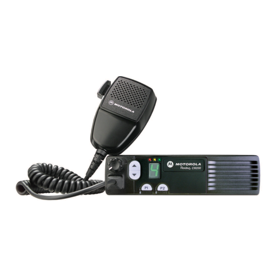
Chapter 1 OVERVIEW CM200 Model The control head contains the internal speaker, the on/off/volume knob, the microphone connector, several buttons to operate the radio, three indicator Light Emitting Diodes (LED) to inform the user about the radio status, and a single character 7-segment display for numeric information e.g. - Page 32 OVERVIEW Notes...
-
Page 33: Chapter 2 Theory Of Operation
This Chapter provides a detailed theory of operation for the Control head circuits. For details of the trouble shooting refer to the related chapter in this section. Control Head Model for CM200 The head contains the internal speaker, the on/off/volume knob, the microphone connector, several buttons to operate the radio and three indicator Light Emitting Diodes (LED) to inform the user about the radio status and a 7-segment display for numeric information. -
Page 34: Keypad Keys
THEORY OF OPERATION When the host radio needs to send date to the shift register, the radio asserts the shift register chip select and the data is loaded to the shift register. For example, the host radio sends data to change display channel or change LED status. -
Page 35: Speaker
Control Head Model for CM200 If the BOOT_RES (J802-7) line is connected to >5V (e.g. 9.3V) at turn-on, the uP will start in boot mode instead of normal operation. This mode is used to programme new firmware into the FLASH memory (U404 mainboard). -
Page 36: Control Head Model For Cm300/Pm400
THEORY OF OPERATION Control Head Model for CM300/PM400 The control head contains the internal speaker, the on/off/volume knob, the microphone connector, several buttons to operate the radio, three indicator Light Emitting Diodes (LED) to inform the user about the radio status, and an 8 character Liquid Crystal Display (LCD) for alpha - numerical information e.g. -
Page 37: Keypad Keys
Control Head Model for CM300/PM400 Keypad Keys The control head keypad is a four-key design. All keys are configured as two analog lines read by µP. The voltage on the analog lines varies between 0V and 3.3 V depending on which key is pressed. -
Page 38: Speaker
THEORY OF OPERATION The HOOK line (J102-6) is used to inform the uP which type of microphone or SCI lead is connected to the microphone socket. The voltage of the HOOK line is monitored by the uP (port PE0, MIC_SENSE) through a resistor divider on the main board. When the HOOK line is grounded (on hook condition) or floating (2.8V nominal), the uP sets the mux (U8) for keypad operation to allow the use of microphones with a keypad. -
Page 39: Control Head Cm200 Troubleshooting Chart
Chapter 3 TROUBLESHOOTING CHARTS Control Head CM200 Troubleshooting Chart Control Head Failure Control Head Check Check 9.3V on Back light R808, R809 OK ? Check Speaker Power-up Alert Tone Connection OK ? Power-up Check Red LED D801, Q806, U801 Flash? -
Page 40: Button/Tones Select Error
TROUBLESHOOTING CHARTS Button/Tones Select Error (Page 1 of 2) Button/Tones Check Check Voltage Levels on TP401 (Keypad Col) and TP402 (Keypad Row) (see table on next page) Right Voltage Check R846, R811 Up Key on Control Head Right Voltage Check R845, R810 on Down Key on Control Head Right... - Page 41 Control Head CM200 Troubleshooting Chart Button/Tones Select Error (Page 2 of 2) Right Does Q812 Voltage on Control Head Replace on DTMF keys operates well Q812 Button/Tones Keys Replace U803 Okay on Control Head Key_Col Key_Column Voltage TP401 Voltage (TP401) 0.008 V...
-
Page 42: Control Head Cm300/Pm400 Troubleshooting Chart
TROUBLESHOOTING CHARTS Control Head CM300/PM400 Troubleshooting Chart Control Head Failure Control Head Check Check 9.3V on Back light Q12, U1 and associated OK ? parts and U8 Power-up Check Speaker Alert Tone Connection OK ? Indicator Check LED’ Q8-Q10, U8 and 9.3V OK ? Display Check LCD... -
Page 43: Button/Tones Select Error
Control Head CM300/PM400 Troubleshooting Chart Button/Tones Select Error (Page 1 of 2) Button/Tones Check Check Voltage Levels on TP401 (Keypad Col) and TP402 (Keypad Row) (see table on next page) Right Check R13, R45 Voltage on Control Head Up Key? Right Check R12, R49 Voltage... - Page 44 TROUBLESHOOTING CHARTS Button/Tones Select Error (Page 2 of 2) Right Does Q41 Voltage on Control Head Replace on DTMF keys operates well Button/Tones Keys Replace U8 Okay on Control Head Key_Col Key_Column Voltage TP401 Voltage (TP401) 0.008 V 0.675 V 1.346 V 1.997 V 2.650 V...
-
Page 45: Allocation Of Schematics And Circuit Boards
CONTROLHEAD PCB / SCHEMATICS / PARTS LISTS Allocation of Schematics and Circuit Boards Table 4-1 Control Head Diagrams and Parts Lists PCB : Control Head CM200 Page 4-3 8488998U01 Main Board Top Side Page 4-3 8488998U01 Main Board Bottom Side... - Page 46 CONTROLHEAD PCB / SCHEMATICS / PARTS LISTS Notes...
-
Page 47: Control Head Cm200 - Pcb 8488998U01 / Schematics
Control Head CM200 - PCB 8488998U01 / Schematics Control Head CM200 - PCB 8488998U01 / Schematics D801 D802 D803 J804 DS801 D806 J805 J802 S802 S801 Top Side SHOWN FROM SIDE 1 8488998u01_p3 Bottom Side Q811 Q804 Q805 Q806 R843... - Page 48 Control Head CM200 - PCB 8488998U01 / Schematics D3_3V R842 R847 C824 C825 M801 10.K 10.K 220.p 100n THESE ARE THE M802 ESD PROTECTION D3_3V M803 CONTACTS (SPRINGS) M804 9_3V C826 C827 R829 R843 DS801 9_3V D3_3V HDSP-513G R821 220.p 100n 10.K...
- Page 49 Control Head CM200 - PCB 8488998U01 / Schematics Control Head PCB 8488998U01 Parts Circuit Motorola Circuit Motorola Description Description List Part No Part No Circuit Motorola M801 7588823L03 PAD GROUNFD LCD R830 0662057A41 CHIP RES 470 OHMS 5% Description Part No...
- Page 50 Control Head CM300/PM400 - PCB 8489714U01 / Schematics Control Head CM300/PM400 - PCB 8489714U01 / Schematics Top Side C35 C36 J103 Bottom Side P101 Control Head CM300/PM400 PCB 8489714U01...
- Page 51 Control Head CM300/PM400 - PCB 8489714U01 / Schematics D3_3V 9_3V COM3 LCD_36PIN COM2 COM1 COM0 5V_IN 9_3V D3_3V CH_PTT D3_3V 5V_IN 5V_CH TELCO_PTT 0.1uF 1000pF 0.1uF 470pF 0.1uF 1000pF 5V_CH 1000pF COM0 220pF 470pF 1000pF MAIN BOARD CONNECTOR COM1 S1D15100 COM2 .022uF J103-14...
- Page 52 Control Head CM300/PM400 - PCB 8489714U01 / Schematics Control Head PCB 8489714U01 Parts List Circuit Motorola Circuit Motorola Circuit Motorola Description Description Description Part No Part No Part No Circuit Motorola Description Part No NOTPLACED CAP, 220pF 7588823L03 CONTACT 0662057A76...
- Page 53 CM200/CM300/PM400 Radios UHF2 (438-470 MHz) 1-25 W Service Information Issue: November, 2007...
- Page 54 Accordingly, any copyrighted Motorola computer programs contained in the Motorola products described in this manual may not be copied or reproduced in any manner without the express written permission of Motorola. Furthermore, the purchase of Motorola...
- Page 55 Table of Contents Chapter 1 MODEL CHART AND TECHNICAL SPECIFICATIONS 1.0 CM200/CM300/PM400 Model Chart..............1-1 2.0 Technical Specifications ..................1-2 Chapter 2 THEORY OF OPERATION 1.0 Introduction ......................2-1 2.0 UHF (438-470 MHz) Receiver ................2-1 2.1 Receiver Front-End..................2-1 2.2 Receiver Back End ..................2-2 3.0 UHF Transmitter Power Amplifier (438-470 MHz) ..........2-2...
- Page 56 8.3 Dual Tone Multiple Frequency (DTMF) Data..........2-18 9.0 Receive Audio Circuits..................2-19 9.1 Squelch Detect ..................2-19 9.2 Audio Processing and Digital Volume Control ........... 2-20 9.3 Audio Amplification Speaker (+) Speaker (-) ..........2-20 9.4 Handset Audio ................... 2-21 9.5 Filtered Audio and Flat Audio ..............
- Page 57 UHF2 (438-470 MHz) 1-25 W Power Control Circuit ........4-18 2.1 UHF2 PCB 8488978U01 (rev. P9) Parts List 1-25 W ........4-19 3.0 UHF 1-25 W Band 2 PCB 8486684Z02 (Rev. A) / Schematics ......4-30 UHF2 Interconnection between Main Board and Power Amplifier Compartment ................4-30 UHF2 (438-470 MHz) 1-25 W 848668Z02 (Rev.
- Page 58 Notes...
-
Page 59: Chapter 1 Model Chart And Technical Specifications
CM300 438-470 MHz, 1-25 W, 32 CH AAM50RNF9AA3AN PM400 438-470 MHz, 1-25 W, 64 CH Item Description PMUE1996_ CM200 Super Tanapa UHF2, 1-25 W, 4 CH PMUE1998_ CM300 Super Tanapa UHF2, 1-25 W, 32 CH PMUE2090_ PM400 Super Tanapa UHF2, 1-25 W, 64 CH FLE1620_... -
Page 60: Technical Specifications
UHF2 Frequency Range: 438-470 MHz Frequency Stability ±2.5 PPM (-30°C to +60°C, 25°C Ref.) Channel Capacity: CM200 - 4 CM300 - 32 PM400 - 64 Channel Spacing: 12.5/20/25 kHz Power Supply: 13.8 Vdc (11 Vdc - 16.6 Vdc) negative Vehicle ground 4.65”... - Page 61 Technical Specifications Transmitter Specification UHF2 Power Output 1-25W Conducted/Radiated -36 dBm < 1 GHz Emissions: -30 dBm > 1 GHz Audio Response: (from 6 dB/ oct. Pre-Emphasis, 300 to TIA603 and CEPT 3000Hz) Tx Audio Distortion < 3% Modulation Limiting: ±2.5 kHz @ 12.5 kHz ±4.0 kHz @ 20 kHz ±5.0 kHz @ 25 kHz...
- Page 62 MODEL CHART AND TECHNICAL SPECIFICATIONS Notes...
-
Page 63: Chapter 2 Theory Of Operation
Chapter 2 THEORY OF OPERATION Introduction This Chapter provides a detailed theory of operation for the UHF circuits in the radio. Details of the theory of operation and trouble shooting for the the associated Controller circuits are included in this Section of the manual. -
Page 64: Receiver Back End
THEORY OF OPERATION Receiver Back End The IF signal from the crystal filter enters the IF amplifier which provides 20 dB of gain and feeds the IF IC at pin 1. The first IF signal at 44.85 MHz mixes with the second local oscillator (LO) at 44.395 MHz to produce the second IF at 455 kHz. -
Page 65: Power Controlled Driver Stage
UHF Transmitter Power Amplifier (438-470 MHz) power of the PA.Op-amp U103-3 monitors the drain current of U101 via resistor R122 and adjusts the bias voltage of U101. In receive mode, the DC voltage from RX_EN line turns on Q101, which in turn switches off the biasing voltage to U101. -
Page 66: Harmonic Filter
THEORY OF OPERATION Harmonic Filter Inductors L111 and L113 along with capacitors C1011, C1023, C1020 and C1016 form a low-pass filter to attenuate harmonic energy coming from the transmitter. Resistor R150 along with L126 drains any electrostatic charges that might otherwise build up on the antenna. The harmonic filter also prevents high level RF signals above the receiver passband from reaching the receiver circuits to improve spurious response rejection. -
Page 67: Fractional-N Synthesizer
UHF (438-470 MHz) Frequency Synthesis This oscillator is temperature compensated to an accuracy of +/-2.5 PPM from -30 to 60 degrees C. The temperature compensation scheme is implemented by an algorithm that uses five crystal parameters (four characterize the inverse Bechmann voltage curve and one for frequency accuracy of the reference oscillator at 25 degrees C). -
Page 68: Voltage Controlled Oscillator (Vco)
THEORY OF OPERATION Voltage Controlled Oscillator (VCO) The Voltage Controlled Oscillator (VCO) consists of the VCO/Buffer IC (VCOBIC, U201), the TX and RX tank circuits, the external RX buffer stages, and the modulation circuitry. AUX3 (U200 Pin 2) U200 Pin 32 Prescaler Out TRB IN Pin 20... -
Page 69: Synthesizer Operation
UHF (438-470 MHz) Frequency Synthesis Synthesizer Operation The synthesizer consists of a low voltage FRAC-N IC (LVFRAC-N), reference oscillator, charge pump circuits, loop filter circuit, and DC supply. The output signal (PRESC_OUT) of the VCOBIC (U201, pin 12) is fed to the PREIN, pin 32 of U200 via a low pass filter which attenuates harmonics and provides a correct input level to the LVFRAC-N in order to close the synthesizer loop. -
Page 70: Controller Theory Of Operation
THEORY OF OPERATION Controller Theory of Operation This section provides a detailed theory of operation for the radio and its components. The main radio is a single-board design, consisting of the transmitter, receiver, and controller circuits. A control head is connected by an extension cable. The control head contains LED indicators, a microphone connector, buttons, and speaker. - Page 71 Controller Theory of Operation The DC voltage applied to connector P2 supplies power directly to the following circuitry: • Electronic on/off control • RF power amplifier • 12 volts P-cH FET -U514 • 9.3 volt regulator • Audio PA Ignition Control Head RF_PA Audio_PA...
-
Page 72: Protection Devices
2-10 THEORY OF OPERATION Voltage regulator U503 provides 5 V for the RF circuits. Input and output capacitors are used to reduce the high frequency noise and provide proper operation during battery transients. Protection Devices Diode VR500 acts as protection against ESD, wrong polarity of the supply voltage, and load dump. VR692 - VR699 are for ESD protection. -
Page 73: Microprocessor Clock Synthesiser
Controller Theory of Operation 2-11 While the radio is switched on, the µP monitors the voltage at the emergency input on the accessory connector via U403-pin 62. Three different conditions are distinguished: no emergency kit is connected, emergency kit connected (unpressed), and emergency press. If no emergency switch is connected or the connection to the emergency switch is broken, the resistive divider R5030 / R5049 will set the voltage to about 3.14 volts (indicates no emergency kit found via EMERGENCY_SENSE line). -
Page 74: Serial Peripheral Interface (Spi)
2-12 THEORY OF OPERATION Serial Peripheral Interface (SPI) The µP communicates to many of the IC’s through its SPI port. This port consists of SPI TRANSMIT DATA (MOSI) (U403-pin100), SPI RECEIVE DATA (MISO) (U403-pin 99), SPI CLK (U0403-pin1) and chip select lines going to the various IC’s, connected on the SPI PORT (BUS). This BUS is a synchronous bus, in that the timing clock signal CLK is sent while SPI data (SPI TRANSMIT DATA or SPI RECEIVE DATA) is sent. -
Page 75: Normal Microprocessor Operation
Controller Theory of Operation 2-13 Normal Microprocessor Operation For this radio, the µP is configured to operate in one of two modes, expanded and bootstrap. In expanded mode the µP uses external memory devices to operate, whereas in bootstrap operation the µP uses only its internal memory. -
Page 76: Static Random Access Memory (Sram)
2-14 THEORY OF OPERATION Static Random Access Memory (SRAM) The SRAM (U402) contains temporary radio calculations or parameters that can change very frequently, and which are generated and stored by the software during its normal operation. The information is lost when the radio is turned off. The device allows an unlimited number of write cycles. -
Page 77: Transmit Audio Circuits
Transmit Audio Circuits 2-15 Transmit Audio Circuits 24kOhms TX SND TX RTN U509 CONTROL HEAD FILTERS AND CONNECTOR PREEMPHASIS ASFIC_CMP GCB3 U504 LIMITER HS SUMMER EXT MIC U509 SPLATTER FLAT TX FILTER AUDIO MOD IN ACCESSORY LS SUMMER CONNECTOR SECTION GCB5 (SYNTHESIZER) ATTENUATOR... -
Page 78: Ptt Sensing And Tx Audio Processing
2-16 THEORY OF OPERATION 7.1.2 Standard Microphone Hook Pin is shorted to the hook mic inside the standard Mic, If the mic is out off hook, 3.3 V is routed to R429 via R458, D401, and it create 0.7 V on MIC_SENSE (u.P U403-67) by Voltage Divider R429/R430. -
Page 79: Transmit Signalling Circuits
Transmit Signalling Circuits 2-17 Transmit Signalling Circuits SUMMER HIGH SPEED 5-3-2 STATE ENCODER CLOCK IN SPLATTER (HSIO) FILTER DTMF MICRO ENCODER CONTROLLER U403 ASFIC_CMP U504 LOW SPEED ENCODER SUMMER CLOCK IN (LSIO) TO RF ATTENUATOR SECTION MOD IN (SYNTHESIZER) Figure 2-8 Transmit Signalling Path From a hardware point of view, there are 3 types of signaling: •... -
Page 80: High Speed Data
2-18 THEORY OF OPERATION High Speed Data High speed data refers to the 3600 baud data waveforms, known as Inbound Signaling Words (ISWs) used in a trunking system for high speed communication between the central controller and the radio. To generate an ISW, the µP first programs the ASFIC CMP (U504) to the proper filter and gain settings. -
Page 81: Receive Audio Circuits
Receive Audio Circuits 2-19 Receive Audio Circuits ACCESSORY CONNECTOR FLT RX AUDIO AUDIO SPKR + EXTERNAL SPKR - U502 SPEAKER SPKR+ SPKR- CONTROL HEAD CONNECTOR MUTE U509 INTERNAL SPEAKER HANDSET AUDIO U505 U IO GCB4 URX OUT AUDIO GCB1 AUX RX VOLUME ASFIC_CMP ATTEN. -
Page 82: Audio Processing And Digital Volume Control
2-20 THEORY OF OPERATION Audio Processing and Digital Volume Control The receiver audio signal (DISC AUDIO) enters the controller section from the IF IC where it is.DC coupled to ASFIC CMP via the DISC input U504-pin 2. The signal is then applied to both the audio and the PL/DPL paths The audio path has a programmable amplifier, whose setting is based on the channel bandwidth being received, an LPF filter to remove any frequency components above 3000 Hz, and a HPF to... -
Page 83: Handset Audio
Receive Signalling Circuits 2-21 Handset Audio Certain handheld accessories have a speaker within them which require a different voltage level than that provided by U502. For these devices HANDSET AUDIO is available at control head connector J2 pin18. The received audio from the output of the ASFIC CMP’s digital volume attenuator is routed to U505 pin 2 where it is amplified. -
Page 84: Alert Tone Circuits
2-22 THEORY OF OPERATION The low speed limited data output (PL, DPL, and trunking LS) appears at U504-pin18, where it connects to the µP U403-pin 80. The low speed data is read by the µP at twice the frequency of the sampling waveform; a latch configuration in the ASFIC CMP stores one bit every clock cycle. -
Page 85: Chapter 3 Troubleshooting Charts
Chapter 3 TROUBLESHOOTING CHARTS This section contains detailed troubleshooting flowcharts. These charts should be used as a guide in determining the problem areas. They are not a substitute for knowledge of circuit operation and astute troubleshooting techniques. It is advisable to refer to the related detailed circuit descriptions in the theory of operation sections prior to troubleshooting a radio. -
Page 86: Troubleshooting Flow Chart For Receiver Rf (Sheet 1 Of 2)
TROUBLESHOOTING CHARTS Troubleshooting Flow Chart for Receiver RF (Sheet 1 of 2) START Problem in 12 KHz and 25 KHz channel spacing 9V on Check Go to R310 (LNA) to U301 Go to RX_EN DC Section Okay ? DC Section Check D301-304 Check Replace IF Filters( FL304, FL301... -
Page 87: Troubleshooting Flow Chart For Receiver (Sheet 2 Of 2)
Troubleshooting Flow Chart for Receiver RF (Sheet 1 of 2) Troubleshooting Flow Chart for Receiver (Sheet 2 of 2) From Check visually FE and BE Go to (IFIC -Vcc) components DC Section OK ? installation ? Inject - 40dBm (CW) Check to RF connector Installation... -
Page 88: Troubleshooting Flow Tx Rf (No Output Power)
TROUBLESHOOTING CHARTS Troubleshooting Flow TX RF (No Output Power) START Key the radio using Radster (type k) Press F6 and read the ASFIC byte Tune the Put 80 Hex in byte #06 Byte PA_BIAS and measure the #04=0 Output Power Replace POUT L108... -
Page 89: Troubleshooting Flow Tx Rf (No Output Power/No Current)
Troubleshooting Flow TX RF (No Output Power) Troubleshooting Flow TX RF (No Output Power/No Current) START Key the radio using Radster (type k) Put 80 Hex in byte #06 and measure the Output Power Replace Measure the Tune the POUT > resistance from PA_BIAS 10 Watts... -
Page 90: Troubleshooting Flow Tx Rf (Not Txing At Nominal Power)
TROUBLESHOOTING CHARTS Troubleshooting Flow TX RF (Not Txing at Nominal power START Key the radio using radster (type k) Press F6 and read the ASFIC byte Is byte Tune the PA_BIAS Measure the resistance #04=0 from R131 to ground Is R131 Tune the K and M factors Repalace PA (Q100) <... -
Page 91: Troubleshooting Flow Chart For Synthesizer
Troubleshooting Flow Chart for Synthesizer Troubleshooting Flow Chart for Synthesizer Start Check 5V at U200 Regulator pins 5, 20, 34 U503 & 36 Visual Correct check of the Problem Board Check D200, D201, C2026, C2025, & C2027 16.8MHz 16.8MHz Replace U200 Pin 47 signal at Signal at U200... -
Page 92: Troubleshooting Flow Chart For Vco
TROUBLESHOOTING CHARTS Troubleshooting Flow Chart for VCO Low or no RF Signal Low or no RF Signal TX VCO RX VCO at input to PA at TP1 Visual check Visual check Correct of board of board Problem Make sure Synthesizer is 4.5V DC 4.5V DC working correctly and runner... -
Page 93: Troubleshooting Flow Chart For Dc Supply (1 Of 2)
Troubleshooting Flow Chart for DC Supply (1 of 2) Troubleshooting Flow Chart for DC Supply (1 of 2) Since the failure of a critical voltage supply might cause the radio to automatically power down, supply voltages should first be probed with a multimeter. If all the board voltages are absent, then the voltage test point should be retested using a rising-edge-triggered oscilloscope. -
Page 94: Troubleshooting Flow Chart For Dc Supply (2 Of 2)
3-10 TROUBLESHOOTING CHARTS Troubleshooting Flow Chart for DC Supply (2 of 2) D3_3V Check VDC on C5007 Go to Digital Section Check Voltage on V=3.3V C5041 Replace U510 Go to Start 9v<V<9.8v... -
Page 95: Allocation Of Schematics And Circuit Boards
Chapter 4 UHF2 PCB/ SCHEMATICS/ PARTS LISTS Allocation of Schematics and Circuit Boards UHF2 and Controller Circuits The UHF circuits are contained on the printed circuit board (PCB) which also contains the Controller circuits. This Chapter shows the schematics for both the UHF circuits and the Controller circuits. The PCB component layouts and the Parts Lists in this Chapter show both the Controller and UHF circuit components. - Page 96 UHF2 PCB/ SCHEMATICS/ PARTS LISTS Notes...
-
Page 97: Uhf 1-25 W Band 2 Pcb 8488978U01 (Rev. P9) / Schematics
UHF 1-25 W Band 2 PCB 8488978U01 (rev. P9) / Schematics UHF 1-25 W Band 2 PCB 8488978U01 (rev. P9) / Schematics TX_INJ TX_INJ FILT_SW_B+ FILT_SW_B+ MAIN COMPARTMENT PA_BIAS PA_BIAS COMP_B+ COMP_B+ DET_VFWD DET_VFWD PWR_SET PWR_SET INTEGRATOR INTEGRATOR RX_EN RX_EN TX_EN TX_EN 73D02968C74-O... -
Page 98: Uhf2 (438-470 Mhz) 1-25 W 8488978U01 (Rev. P9), Top Side
UHF 1-25 W Band 2 PCB 8488978U01 (rev. P9) / Schematics 8488978U01_P9 L119 C1001 C5100 C1097 VR693 C1113 C1026 C1088 L126 L122 VR501 C1008 VR500 R106 L120 C1114 C1016 C1098 R5082 C1154 L111 C1009 R5081 C5096 R5083 C1004 C1087 M102 C1033 R178 C1151... -
Page 99: Uhf2 (438-470 Mhz) 1-25 W 8488978U01 (Rev. P9), Bottom Side
UHF 1-25 W Band 2 PCB 8488978U01 (rev. P9) / Schematics 8488978u01_p9 C5000 R127 C5086 U102 R128 C1061 R126 L115 L117 C1002 D402 VR692 R147 R175 C1106 R131 R403 R404 C5083 L121 VR503 M111 R405 R421 C5060 L500 C1027 R5049 C5055 C1086 R5030... -
Page 100: Uhf2 (438-470 Mhz) 1-25 W Main Circuit (Sht 1 Of 2)
UHF 1-25 W Band 2 PCB 8488978U01 (rev. P9) / Schematics D3_3V FILT_SW_B+ FILT_SW_B+ D3_3V TX_EN SPI_CLK SPI_MOSI SPI_MISO RX_EN LOC_DIST RSSI SYNTH_CS SYNTH_LOCK ASFIC_CS DIGITAL CH_ACT SQ_DET LSIO HSIO F1200 uP_CLK VS_AUDIO_SEL J3 - RESET D3_3V J3-17 J3-4 SERIAL CLOCK VOICE STORAGE AUDIO SELECT J3-16 J3-12... -
Page 101: Uhf2 (438-470 Mhz) 1-25 W Main Circuit (Sht 2 Of 2)
UHF 1-25 W Band 2 PCB 8488978U01 (rev. P9) / Schematics RX_EN TX_EN COMP_B+ (SOURCE) (SOURCE) (SOURCE) PA_BIAS D3_3V D3_3V COMP_B+ SPI_MOSI PA_BIAS PWR_SET SPI_CLK ASFIC_CS PWR_SET FILT_SW_B+ FILT_SW_B+ (SOURCE) CH_ACT FILT_SW_B+ SQ_DET (SOURCE) LSIO FILT_SW_B+ HSIO POWER CONTROL F1200 DET_VFWD INTEGRATOR INTEGRATOR... -
Page 102: Uhf2 (438-470 Mhz) 1-25 W Transmitter (Sht 1 Of 2)
UHF 1-25 W Band 2 PCB 8488978U01 (rev. P9) / Schematics PA_FILT_B+ (SOURCE) IF108 L100 Place inside of the PA compartment 1019447 L119 1019447 COMP_B+ R186 IF109 R137 C1000 C1112 C1111 C1110 C1109 C1106 C1089 C1107 C1103 C1115 C1099 C1100 C1116 39.K 120.p... -
Page 103: Uhf2 (438-470 Mhz) 1-25 W Transmitter (Sht 2 Of 2)
UHF 1-25 W Band 2 PCB 8488978U01 (rev. P9) / Schematics U102 LM2904 Current sense protection (option) FILT_SW_B+_PA C1073 120.p CONTACTS FOR PA CLIP PLTD_HOLE3_5x7_0_TRIMMED L117 1019447 L115 C1002 100.p 18.n Coupler C1011 L113 Antenna Connector width 2.032 39.p D104 17.n J11-1 L111... -
Page 104: Uhf2 (438-470 Mhz) 1-25 W Synthesiser And Vco (Sht 1 Of 2)
4-10 UHF 1-25 W Band 2 PCB 8488978U01 (rev. P9) / Schematics L217 C2026 390nH R225 C2000 C2015 C2034 150. 2.2uF 0.1uF 120.p C2055 C2025 R228 100. C2024 D200 L200 C2198 390nH R226 C2016 C2004 150. C2027 D201 C2005 C2023 C2035 0.1uF 2.2uF... -
Page 105: Uhf2 (438-470 Mhz) 1-25 W Synthesiser And Vco (Sht 2 Of 2)
UHF 1-25 W Band 2 PCB 8488978U01 (rev. P9) / Schematics 4-11 V_SF L201 R231 680nH L209 R220 100.0n 510. R235 C2040 C2042 C2041 C2009 C2038 C2008 C2007 C2011 100n 120.p 120.p 0.1uF 0.1uF 120.p 120.p 0.1uF V_SF C2021 L208 100.0n C2010 C2039... -
Page 106: Uhf2 (438-470 Mhz) 1-25 W Receiver Front And Back End (Sht 1 Of 2)
4-12 UHF 1-25 W Band 2 PCB 8488978U01 (rev. P9) / Schematics FRONT-END SHIELD Q304 Q306 R334 R300 430. R310 R346 LOC_DIST 10.K 10.K 15.K C321 120.p R345 10.K Q300 R336 L304 220. C323 C350 150.n RX_EN 120.p Q301 D305 MIXER SHIELD L301 R331... -
Page 107: Uhf2 (438-470 Mhz) 1-25 W Receiver Front And Back End (Sht 2 Of 2)
UHF 1-25 W Band 2 PCB 8488978U01 (rev. P9) / Schematics 4-13 R315 R306 U301 12.K 20.K FL301 TC7W04F FLTR C313 1 IN 100n U301 TC7W04F BW_SEL R316 D302 D301 FL302 R305 12.K 20.K FLTR C312 Check if it is 3v or another value 100n 1 IN R314... -
Page 108: Uhf2 (438-470 Mhz) 1-25 W Dc And Audio Circuits (Sht 1 Of 2)
4-14 UHF 1-25 W Band 2 PCB 8488978U01 (rev. P9) / Schematics L120 1019447 IF502 COMP_B+ IF503 SOURCE C1113 C1097 C1088 C1098 C1114 L500 FILT_B+ 39.p 39.p 120.p 120.p 39.p 1019447 U501 9.3V POWER SUPPLY 9.3V SOURCE LM2941T IF505 VOUT ON_OFF R5081 6.34K... -
Page 109: Uhf2 (438-470 Mhz) 1-25 W Dc And Audio Circuits (Sht 2 Of 2)
UHF 1-25 W Band 2 PCB 8488978U01 (rev. P9) / Schematics 4-15 C5089 82.p C5090 82.p R5024 R5068 R5046 24.K R5022 100.K POST_LIMITER_FLAT_TX_AUDIO_RETURN_OPT_BRD 100.K 6.2K U506 R5045 R5056 C5056 LM2904 33.K 10.K U506 C5081 C5033 LM2904 C5101 120.p 100n R5023 C5032 FLAT_TX_AUDIO_INPUT_ACCESS_CONN 100.K... -
Page 110: Uhf2 (438-470 Mhz) 1-25 W Microprocessor And Controller Circuits (Sht 1 Of 2)
4-16 UHF 1-25 W Band 2 PCB 8488978U01 (rev. P9) / Schematics D400 D3_3V R462 SCI_CH C410 TP406 R450 TEST_POINT R451 100n R439 LSIO 10.K 10.K 10.K SPI_MISO CH_ACT TP410 TP404 TEST_POINT TEST_POINT SPI_MOSI SQ_DET SPI_CLK HSIO ASFIC_CS OPT_DATA_R_OPBD Q407 Q400 D3_3V SYNTH_CS... -
Page 111: Uhf2 (438-470 Mhz) 1-25 W Microprocessor And Controller Circuits (Sht 2 Of 2)
UHF 1-25 W Band 2 PCB 8488978U01 (rev. P9) / Schematics 4-17 FILT_SW_B+ R401 R460 Q403 2.7K 1.5K D3_3V PROG_OUT-ALARM_4 R444 10.K TP405 Q401 TEST_POINT D3_3V BOOT_EN_IN_CH Q415 D3_3V R431 R436 R457 VR400 10.K 33.K Q412 3.3K 6.80 ACCESS_PTT C490 R459 47.K R458... -
Page 112: Uhf2 (438-470 Mhz) 1-25 W Power Control Circuit
4-18 UHF 1-25 W Band 2 PCB 8488978U01 (rev. P9) / Schematics FILT_SW_B+ U100 LM2904 IF701 L101 INTEGRATOR IF700 DET_VFWD C1046 R141 120.p 22.K C1071 120.p C1082 C1045 C1075 39.p 120.p 39.p R117 R140 27.K U100 LM2904 73D02968C74-O SHEET 3 OF 8 UHF2 (438-470 MHz) 1-25 W Power Control Circuit... -
Page 113: Uhf2 Pcb 8488978U01 (Rev. P9) Parts List 1-25 W
UHF 1-25 W Band 2 PCB 8488978U01 (rev. P9) / Schematics 4-19 2.1 UHF2 PCB 8488978U01 (rev. P9) Parts Circuit Motorola Circuit Motorola Circuit Motorola Description Description Description List 1-25 W Ref. Part No. Ref. Part No. Ref. Part No. - Page 114 4-20 UHF 1-25 W Band 2 PCB 8488978U01 (rev. P9) / Schematics Circuit Motorola Circuit Motorola Circuit Motorola Circuit Motorola Description Description Description Description Ref. Part No. Ref. Part No. Ref. Part No. Ref. Part No. C1098 2113740F53 CAP CHIP REEL CL1 +/-...
- Page 115 UHF 1-25 W Band 2 PCB 8488978U01 (rev. P9) / Schematics 4-21 Circuit Motorola Circuit Motorola Circuit Motorola Circuit Motorola Description Description Description Description Ref. Part No. Ref. Part No. Ref. Part No. Ref. Part No. C2043 2113740L14 CAP CER CHIP 6.8PF +-...
- Page 116 4-22 UHF 1-25 W Band 2 PCB 8488978U01 (rev. P9) / Schematics Circuit Motorola Circuit Motorola Circuit Motorola Circuit Motorola Description Description Description Description Ref. Part No. Ref. Part No. Ref. Part No. Ref. Part No. C345 2113740L08 CAP CER CHIP 3.9 PF+/-...
- Page 117 UHF 1-25 W Band 2 PCB 8488978U01 (rev. P9) / Schematics 4-23 Circuit Motorola Circuit Motorola Circuit Motorola Circuit Motorola Description Description Description Description Ref. Part No. Ref. Part No. Ref. Part No. Ref. Part No. C5046 2113743E20 CAP CHIP. 10 UF 10%...
- Page 118 4-24 UHF 1-25 W Band 2 PCB 8488978U01 (rev. P9) / Schematics Circuit Motorola Circuit Motorola Circuit Motorola Circuit Motorola Description Description Description Description Ref. Part No. Ref. Part No. Ref. Part No. Ref. Part No. C611 2113740F41 CAP CHIP REEL CL1 +/-...
- Page 119 UHF 1-25 W Band 2 PCB 8488978U01 (rev. P9) / Schematics 4-25 Circuit Motorola Circuit Motorola Circuit Motorola Circuit Motorola Description Description Description Description Ref. Part No. Ref. Part No. Ref. Part No. Ref. Part No. L209 2413926N24 IND CER CHIP 100.0 NH...
- Page 120 4-26 UHF 1-25 W Band 2 PCB 8488978U01 (rev. P9) / Schematics Circuit Motorola Circuit Motorola Circuit Motorola Circuit Motorola Description Description Description Description Ref. Part No. Ref. Part No. Ref. Part No. Ref. Part No. R127 0662057C03 CHIP RES 1.0 OHMS 5%...
- Page 121 UHF 1-25 W Band 2 PCB 8488978U01 (rev. P9) / Schematics 4-27 Circuit Motorola Circuit Motorola Circuit Motorola Circuit Motorola Description Description Description Description Ref. Part No. Ref. Part No. Ref. Part No. Ref. Part No. R320 0662057A73 CHIP RES 10K OHMS 5%...
- Page 122 4-28 UHF 1-25 W Band 2 PCB 8488978U01 (rev. P9) / Schematics Circuit Motorola Circuit Motorola Circuit Motorola Circuit Motorola Description Description Description Description Ref. Part No. Ref. Part No. Ref. Part No. Ref. Part No. R5023 0662057A97 CHIP RES 100K OHMS...
- Page 123 UHF 1-25 W Band 2 PCB 8488978U01 (rev. P9) / Schematics 4-29 Circuit Motorola Circuit Motorola Circuit Motorola Description Description Description Ref. Part No. Ref. Part No. Ref. Part No. U102 5113818A01 IC LOW COST SING U509 5113806A20 IC MUX/DEMUX TRIPLE...
-
Page 124: Uhf 1-25 W Band 2 Pcb 8486684Z02 (Rev. A) / Schematics
4-30 UHF 1-25 W Band 2 PCB 8486684Z02 (Rev. A) / Schematics UHF 1-25 W Band 2 PCB 8486684Z02 (Rev. A) / Schematics TX_INJ TX_INJ FILT_SW_B+ FILT_SW_B+ MAIN COMPARTMENT PA_BIAS PA_BIAS COMP_B+ COMP_B+ DET_VFWD DET_VFWD PWR_SET PWR_SET INTEGRATOR INTEGRATOR RX_EN RX_EN TX_EN TX_EN... -
Page 125: Uhf2 (438-470 Mhz) 1-25 W 848668Z02 (Rev. A), Top Side
UHF 1-25 W Band 2 PCB 8486684Z02 (Rev. A) / Schematics 4-31 C5100 C1001 C1097 VR693 C1113 C1088 L126 VR501 C1008 VR500 C1114 C1016 C1098 R5082 R5081 C5096 C1154 R5083 C1009 M102 C1087 C1033 R178 C1084 C1151 M100 C1063 R179 C1129 C5001 R5074... -
Page 126: Uhf2 (438-470 Mhz) 1-25 W 848668Z02 (Rev. A) , Bottom Side
4-32 UHF 1-25 W Band 2 PCB 8486684Z02 (Rev. A) / Schematics C5000 R127 C5086 C1061 R128 D402 L115 R126 VR692 R147 R175 C1106 R131 R403 R404 VR503 C5083 R405 R421 L500 R5049 C5055 C5060 C1086 R5020 R5030 C1128 C5037 R5036 R5023 C1127... -
Page 127: Uhf2 (438-470 Mhz) 1-25 W Main Circuit (Sht 1 Of 2)
UHF 1-25 W Band 2 PCB 8486684Z02 (Rev. A) / Schematics 4-33 D3_3V FILT_SW_B+ FILT_SW_B+ D3_3V TX_EN SPI_CLK SPI_MOSI SPI_MISO RX_EN LOC_DIST RSSI SYNTH_CS SYNTH_LOCK ASFIC_CS DIGITAL CH_ACT SQ_DET LSIO HSIO F1200 uP_CLK VS_AUDIO_SEL J3 - RESET D3_3V J3-17 J3-4 VOICE STORAGE AUDIO SELECT SERIAL CLOCK J3-16... -
Page 128: Uhf2 (438-470 Mhz) 1-25 W Main Circuit (Sht 2 Of 2)
4-34 UHF 1-25 W Band 2 PCB 8486684Z02 (Rev. A) / Schematics RX_EN TX_EN COMP_B+ (SOURCE) (SOURCE) (SOURCE) PA_BIAS D3_3V COMP_B+ SPI_MOSI D3_3V PA_BIAS PWR_SET SPI_CLK ASFIC_CS PWR_SET FILT_SW_B+ FILT_SW_B+ (SOURCE) CH_ACT FILT_SW_B+ SQ_DET (SOURCE) LSIO FILT_SW_B+ HSIO POWER CONTROL F1200 DET_VFWD INTEGRATOR... -
Page 129: Uhf2 (438-470 Mhz) 1-25 W Transmitter (Sht 1 Of 2)
UHF 1-25 W Band 2 PCB 8486684Z02 (Rev. A) / Schematics 4-35 PA_FILT_B+ (SOURCE) IF108 Place inside of the PA compartment L100 1019447 L119 1019447 COMP_B+ R186 IF109 R137 C1089 C1116 C1000 C1112 C1111 C1110 C1109 C1106 C1107 C1103 C1115 C1099 C1100 39.p... -
Page 130: Uhf2 (438-470 Mhz) 1-25 W Transmitter (Sht 2 Of 2)
4-36 UHF 1-25 W Band 2 PCB 8486684Z02 (Rev. A) / Schematics U102 LM2904 Current sense protection (option) FILT_SW_B+_PA C1073 120.p CONTACTS FOR PA CLIP PLTD_HOLE3_5x7_0_TRIMMED L117 1019447 L115 C1002 18.n 100.p Coupler C1011 L113 Antenna Connector width 2.032 39.p D104 17.n J11-1... -
Page 131: Uhf2 (438-470 Mhz) 1-25 W Synthesiser And Vco (Sht 1 Of 2)
UHF 1-25 W Band 2 PCB 8486684Z02 (Rev. A) / Schematics 4-37 L217 C2026 390nH R225 C2034 C2000 C2015 150. 120.p 2.2uF 0.1uF C2055 C2025 R228 100. C2024 D200 L200 390nH C2198 R226 C2016 C2004 150. D201 C2005 C2023 C2035 0.1uF 2.2uF C2027... -
Page 132: Uhf2 (438-470 Mhz) 1-25 W Synthesiser And Vco (Sht 2 Of 2)
4-38 UHF 1-25 W Band 2 PCB 8486684Z02 (Rev. A) / Schematics V_SF L201 R231 680nH L209 R220 100.0n 510. C2011 C2040 C2042 C2041 C2009 C2038 C2008 C2007 R235 0.1uF 100n 120.p 0.1uF 0.1uF 120.p 120.p 120.p V_SF C2021 L208 100.0n C2010 C2039... -
Page 133: Uhf2 (438-470 Mhz) 1-25 W Receiver Front And Back End (Sht 1 Of 2)
UHF 1-25 W Band 2 PCB 8486684Z02 (Rev. A) / Schematics 4-39 FRONT-END SHIELD Q304 Q306 R334 430. R346 R300 R310 LOC_DIST 10.K 10.K 15.K C321 120.p R345 10.K Q300 R336 220. L304 C323 C350 150.n RX_EN 120.p Q301 D305 MIXER SHIELD L301 R331... -
Page 134: Uhf2 (438-470 Mhz) 1-25 W Receiver Front And Back End (Sht 2 Of 2)
4-40 UHF 1-25 W Band 2 PCB 8486684Z02 (Rev. A) / Schematics R315 R306 U301 FL301 12.K 20.K TC7W04F FLTR C313 1 IN 100n U301 TC7W04F BW_SEL D302 R316 D301 FL302 R305 12.K FLTR 20.K C312 Check if it is 3v or another value 100n 1 IN R314... -
Page 135: Uhf2 (438-470 Mhz) 1-25 W Dc And Audio Circuits (Sht 1 Of 2)
UHF 1-25 W Band 2 PCB 8486684Z02 (Rev. A) / Schematics 4-41 L120 1019447 IF502 COMP_B+ IF503 SOURCE C1113 C1097 C1088 C1098 C1114 FILT_B+ L500 39.p 39.p 120.p 120.p 39.p 1019447 U501 9.3V POWER SUPPLY 9.3V SOURCE IF505 LM2941T VOUT ON_OFF R5081 6.34K... -
Page 136: Uhf2 (438-470 Mhz) 1-25 W Dc And Audio Circuits (Sht 2 Of 2)
4-42 UHF 1-25 W Band 2 PCB 8486684Z02 (Rev. A) / Schematics C5089 82.p C5090 82.p R5024 R5068 R5046 24.K R5022 100.K POST_LIMITER_FLAT_TX_AUDIO_RETURN_OPT_BRD 100.K 6.2K U506 R5045 R5056 C5056 LM2904 33.K 10.K U506 C5033 C5081 LM2904 C5101 120.p 100n R5023 C5032 FLAT_TX_AUDIO_INPUT_ACCESS_CONN 100.K... -
Page 137: Uhf2 (438-470 Mhz) 1-25 W Microprocessor And Controller Circuits (Sht 1 Of 2)
UHF 1-25 W Band 2 PCB 8486684Z02 (Rev. A) / Schematics 4-43 D400 D3_3V R462 SCI_CH C410 TP406 R450 TEST_POINT R451 R439 100n LSIO 10.K 10.K 10.K SPI_MISO CH_ACT TP410 TP404 TEST_POINT TEST_POINT SPI_MOSI SQ_DET SPI_CLK HSIO ASFIC_CS OPT_DATA_R_OPBD Q407 Q400 D3_3V SYNTH_CS... -
Page 138: Uhf2 (438-470 Mhz) 1-25 W Microprocessor And Controller Circuits (Sht 2 Of 2)
4-44 UHF 1-25 W Band 2 PCB 8486684Z02 (Rev. A) / Schematics FILT_SW_B+ R401 R460 Q403 2.7K 1.5K D3_3V PROG_OUT-ALARM_4 R444 TP405 10.K Q401 TEST_POINT D3_3V BOOT_EN_IN_CH Q415 D3_3V R431 R436 R457 10.K VR400 33.K Q412 3.3K 6.80 ACCESS_PTT C490 R459 47.K R458... -
Page 139: Uhf2 (438-470 Mhz) 1-25 W Power Control Circuit
UHF 1-25 W Band 2 PCB 8486684Z02 (Rev. A) / Schematics 4-45 FILT_SW_B+ U100 LM2904 IF701 L101 INTEGRATOR IF700 C1046 DET_VFWD R141 120.p 22.K C1071 120.p C1082 C1045 C1075 39.p 120.p 39.p R117 R140 27.K U100 LM2904 73D02968C74-O SHEET 3 OF 8 UHF2 (438-470 MHz) 1-25 W Power Control Circuit... -
Page 140: Uhf2 Pcb 8486684Z02 (Rev. A) Parts List 1-25 W
4-46 UHF 1-25 W Band 2 PCB 8486684Z02 (Rev. A) / Schematics UHF2 PCB 8486684Z02 (Rev. A) Parts Circuit Motorola Part Circuit Motorola Part Circuit Motorola Part List 1-25 W Description Description Description Ref. Ref. Ref. Circuit Motorola Part C1054... - Page 141 UHF 1-25 W Band 2 PCB 8486684Z02 (Rev. A) / Schematics 4-47 Circuit Motorola Part Circuit Motorola Part Circuit Motorola Part Circuit Motorola Part Description Description Description Description Ref. Ref. Ref. Ref. C1099 2113740F53 CAP CHIP REEL CL1 +/- C1121...
- Page 142 4-48 UHF 1-25 W Band 2 PCB 8486684Z02 (Rev. A) / Schematics Circuit Motorola Part Circuit Motorola Part Circuit Motorola Part Circuit Motorola Part Description Description Description Description Ref. Ref. Ref. Ref. C2041 2113740F53 CAP CHIP REEL CL1 +/- C2061...
- Page 143 UHF 1-25 W Band 2 PCB 8486684Z02 (Rev. A) / Schematics 4-49 Circuit Motorola Part Circuit Motorola Part Circuit Motorola Part Circuit Motorola Part Description Description Description Description Ref. Ref. Ref. Ref. C347 2113740L07 CAP CER CHIP 3.6PF +- C369...
- Page 144 4-50 UHF 1-25 W Band 2 PCB 8486684Z02 (Rev. A) / Schematics Circuit Motorola Part Circuit Motorola Part Circuit Motorola Part Circuit Motorola Part Description Description Description Description Ref. Ref. Ref. Ref. C5049 2113743E20 CAP CHIP. 10 UF 10% C5069...
- Page 145 UHF 1-25 W Band 2 PCB 8486684Z02 (Rev. A) / Schematics 4-51 Circuit Motorola Part Circuit Motorola Part Circuit Motorola Part Circuit Motorola Part Description Description Description Description Ref. Ref. Ref. Ref. C613 2113740F41 CAP CHIP REEL CL1 +/- C632...
- Page 146 4-52 UHF 1-25 W Band 2 PCB 8486684Z02 (Rev. A) / Schematics Circuit Motorola Part Circuit Motorola Part Circuit Motorola Part Circuit Motorola Part Description Description Description Description Ref. Ref. Ref. Ref. L211 2413926N24 IND CER CHIP 100.0 NH L315...
- Page 147 UHF 1-25 W Band 2 PCB 8486684Z02 (Rev. A) / Schematics 4-53 Circuit Motorola Part Circuit Motorola Part Circuit Motorola Part Circuit Motorola Part Description Description Description Description Ref. Ref. Ref. Ref. R130 0662057B47 CHIP RES 0 OHMS +-.050 R165...
- Page 148 4-54 UHF 1-25 W Band 2 PCB 8486684Z02 (Rev. A) / Schematics Circuit Motorola Part Circuit Motorola Part Circuit Motorola Part Circuit Motorola Part Description Description Description Description Ref. Ref. Ref. Ref. R321 0662057A71 CHIP RES 8200 OHMS R403 0662057B47 CHIP RES 0 OHMS +-.050...
- Page 149 R5074 0662057A49 CHIP RES 1000 OHMS R5098 NOT PLACED GCAM DUMMY PART R5051 0662057A75 CHIP RES 12K OHMS 5% 5% (Not used in CM200) NUMBER R5052 0662057A73 CHIP RES 10K OHMS 5% R5025 0662057A97 CHIP RES 100K OHMS R5075 0662057A42...
- Page 150 NUMBER U515 5162852A59 IC CMOS ANALOG PIN GFP SWITCH SPDT (Not used R5098 NOT PLACED GCAM DUMMY PART Y201 4880114R06 CRYSTAL 16.8MHZ in CM200) U201 5105750U54 IC PKG DIE VCO NUMBER Y300 9186145B02 CER.DISCR. BUFFER VR101 4813830A18 DIODE 6.8V 5%...
- Page 151 CM200/CM300/PM400 Radios UHF2 (438-470 MHz) 25-40 W Service Information Issue: November, 2007...
- Page 152 Accordingly, any copyrighted Motorola computer programs contained in the Motorola products described in this manual may not be copied or reproduced in any manner without the express written permission of Motorola. Furthermore, the purchase of Motorola...
- Page 153 Table of Contents Chapter 1 MODEL CHART AND TECHNICAL SPECIFICATIONS 1.0 CM200/CM300/PM400 Model Chart..............1-1 2.0 Technical Specifications ..................1-2 Chapter 2 THEORY OF OPERATION 1.0 Introduction ......................2-1 2.0 UHF (438-470 MHz) Receiver ................2-1 2.1 Receiver Front-End..................2-1 2.2 Receiver Back End ..................2-2 3.0 UHF Transmitter Power Amplifier (438-470 MHz) ..........2-2...
- Page 154 9.0 Receive Audio Circuits..................2-19 9.1 Squelch Detect ..................2-19 9.2 Audio Processing and Digital Volume Control ........... 2-20 9.3 Audio Amplification Speaker (+) Speaker (-) ..........2-20 9.4 Handset Audio ................... 2-21 9.5 Filtered Audio and Flat Audio ..............2-21 10.0 Receive Signalling Circuits ................
- Page 155 3.0 UHF 25-40 W Band 4 PCB 8486577Z03 / Schematics ........4-31 UHF2 Interconnection between Main Board and Power Amplifier Compartment ..................4-31 UHF 2 (438-470 MHz) 25-40 W 8486577Z03, Top Side ........4-32 UHF2 (438-470 MHz) 25-40 W 8486577Z03, Bottom Side ......4-33 UHF2 (438-470 MHz) 25-40 W Main Circuit (Sht 1 of 2) ........4-34 UHF2 (438-470 MHz) 25-40 W Main Circuit (Sht 2 of 2) ........4-35 UHF2 (438-470 MHz) 25-40 W Transmitter (Sht 1 of 2) ........4-36...
- Page 156 Notes...
-
Page 157: Chapter 1 Model Chart And Technical Specifications
CM300 438-470 MHz, 25-40 W, 32 CH AAM50RPF9AA3AN PM400 438-470 MHz, 25-40 W, 64 CH Item Description PMUE2007_ CM200 Super Tanapa UHF2, 25-40 W, 4 CH PMUE2010_ CM300 Super Tanapa UHF2, 25-40 W, 32 CH PMUE2091_ PM400 Super Tanapa UHF2, 25-40 W, 64 CH PMUE2032_... -
Page 158: Technical Specifications
UHF2 Frequency Range: 438-470 MHz Frequency Stability ±2.5 PPM (-30°C to +60°C, 25°C Ref.) Channel Capacity: CM200 - 4 CM300 - 32 PM400 - 64 Channel Spacing: 12.5/25 kHz Power Supply: 13.6 Vdc (10.88 Vdc - 16.32 Vdc) negative Vehicle ground 4.65”... - Page 159 Technical Specifications Transmitter Specification UHF2 Power Output 25-40W Conducted/Radiated -26 dBm Emissions: Audio Response: (from 6 dB/ oct. Pre-Emphasis, 300 to TIA603 and CEPT 3000Hz) Tx Audio Distortion < 3% Modulation Limiting: ±2.5 kHz @ 12.5 kHz ±4.0 kHz @ 20 kHz ±5.0 kHz @ 25 kHz FM Hum and Noise: -35 dB@12.5 kHz...
- Page 160 MODEL CHART AND TECHNICAL SPECIFICATIONS Notes...
-
Page 161: Chapter 2 Theory Of Operation
Chapter 2 THEORY OF OPERATION Introduction This Chapter provides a detailed theory of operation for the UHF circuits in the radio. Details of the theory of operation and trouble shooting for the the associated Controller circuits are included in this Section of the manual. -
Page 162: Receiver Back End
THEORY OF OPERATION Receiver Back End The IF signal from the crystal filter enters the IF amplifier which provides 20 dB of gain and feeds the IF IC at pin 1. The first IF signal at 44.85 MHz mixes with the second local oscillator (LO) at 44.395 MHz to produce the second IF at 455 kHz. -
Page 163: Power Controlled Driver Stage
UHF Transmitter Power Amplifier (438-470 MHz) power of the PA.Op-amp U103-3 monitors the drain current of U101 via resistor R122 and adjusts the bias voltage of U101. In receive mode, the DC voltage from RX_EN line turns on Q101, which in turn switches off the biasing voltage to U101. -
Page 164: Harmonic Filter
THEORY OF OPERATION Harmonic Filter Inductors L111, L113 and L128 along with capacitors C1011, C1023, C1020, C1016, C1025 and C1026 form a low-pass filter to attenuate harmonic energy coming from the transmitter. Resistor R150 along with L130 drains any electrostatic charges that might otherwise build up on the antenna. The harmonic filter also prevents high level RF signals above the receiver passband from reaching the receiver circuits to improve spurious response rejection. -
Page 165: Fractional-N Synthesizer
UHF (438-470 MHz) Frequency Synthesizer parameters (four characterize the inverse Bechmann voltage curve and one for frequency accuracy of the reference oscillator at 25 degrees C). This algorithm is implemented by the LVFRAC-N (U200) at the power up of the radio. TCXO Y200, along with its corresponding circuitry R204, R205, R210, and C2053, are not placed as the temperature compensated crystal proved to be reliable. -
Page 166: Voltage Controlled Oscillator (Vco)
THEORY OF OPERATION Voltage Controlled Oscillator (VCO) The Voltage Controlled Oscillator (VCO) consists of the VCO/Buffer IC (VCOBIC, U201), the TX and RX tank circuits, the external RX buffer stages, and the modulation circuitry. AUX3 (U200 Pin 2) U200 Pin 32 Prescaler Out TRB IN Pin 20... -
Page 167: Synthesizer Operation
UHF (438-470 MHz) Frequency Synthesizer Synthesizer Operation The synthesizer consists of a low voltage FRAC-N IC (LVFRAC-N), reference oscillator, charge pump circuits, loop filter circuit, and DC supply. The output signal (PRESC_OUT) of the VCOBIC (U201, pin 12) is fed to the PREIN, pin 32 of U200 via a low pass filter which attenuates harmonics and provides a correct input level to the LVFRAC-N in order to close the synthesizer loop. -
Page 168: Controller Theory Of Operation
THEORY OF OPERATION Controller Theory of Operation This section provides a detailed theory of operation for the radio and its components. The main radio is a single-board design, consisting of the transmitter, receiver, and controller circuits. A control head is connected by an extension cable. The control head contains LED indicators, a microphone connector, buttons, and speaker. - Page 169 Controller Theory of Operation The DC voltage applied to connector P2 supplies power directly to the following circuitry: • Electronic on/off control • RF power amplifier • 12 volts P-cH FET -U514 • 9.3 volt regulator • Audio PA Ignition Control Head RF_PA, 8.5 A Audio_PA...
-
Page 170: Protection Devices
2-10 THEORY OF OPERATION Voltage regulator U503 provides 5 V for the RF circuits. Input and output capacitors are used to reduce the high frequency noise and provide proper operation during battery transients. Protection Devices Diode VR500 acts as protection against ESD, wrong polarity of the supply voltage, and load dump. VR692 - VR699 are for ESD protection. -
Page 171: Microprocessor Clock Synthesiser
Controller Theory of Operation 2-11 While the radio is switched on, the µP monitors the voltage at the emergency input on the accessory connector via U403-pin 62. Three different conditions are distinguished: no emergency kit is connected, emergency kit connected (unpressed), and emergency press. If no emergency switch is connected or the connection to the emergency switch is broken, the resistive divider R5030 / R5049 will set the voltage to about 3.14 volts (indicates no emergency kit found via EMERGENCY_SENSE line). -
Page 172: Serial Peripheral Interface (Spi)
2-12 THEORY OF OPERATION Serial Peripheral Interface (SPI) The µP communicates to many of the IC’s through its SPI port. This port consists of SPI TRANSMIT DATA (MOSI) (U403-pin100), SPI RECEIVE DATA (MISO) (U403-pin 99), SPI CLK (U0403-pin1) and chip select lines going to the various IC’s, connected on the SPI PORT (BUS). This BUS is a synchronous bus, in that the timing clock signal CLK is sent while SPI data (SPI TRANSMIT DATA or SPI RECEIVE DATA) is sent. -
Page 173: Normal Microprocessor Operation
Controller Theory of Operation 2-13 Normal Microprocessor Operation For this radio, the µP is configured to operate in one of two modes, expanded and bootstrap. In expanded mode the µP uses external memory devices to operate, whereas in bootstrap operation the µP uses only its internal memory. -
Page 174: Static Random Access Memory (Sram)
2-14 THEORY OF OPERATION Static Random Access Memory (SRAM) The SRAM (U402) contains temporary radio calculations or parameters that can change very frequently, and which are generated and stored by the software during its normal operation. The information is lost when the radio is turned off. The device allows an unlimited number of write cycles. -
Page 175: Transmit Audio Circuits
Transmit Audio Circuits 2-15 Transmit Audio Circuits 24kOhms TX SND TX RTN U509 CONTROL HEAD FILTERS AND CONNECTOR PREEMPHASIS ASFIC_CMP GCB3 U504 LIMITER HS SUMMER EXT MIC U509 SPLATTER FLAT TX FILTER AUDIO MOD IN ACCESSORY LS SUMMER CONNECTOR SECTION GCB5 (SYNTHESIZER) ATTENUATOR... -
Page 176: Ptt Sensing And Tx Audio Processing
2-16 THEORY OF OPERATION 7.1.2 Standard Microphone Hook Pin is shorted to the hook mic inside the standard Mic, If the mic is out off hook, 3.3 V is routed to R429 via R458, D401, and it create 0.7 V on MIC_SENSE (u.P U403-67) by Voltage Divider R429/R430. -
Page 177: Transmit Signalling Circuits
Transmit Signalling Circuits 2-17 Transmit Signalling Circuits SUMMER HIGH SPEED 5-3-2 STATE ENCODER CLOCK IN SPLATTER (HSIO) FILTER DTMF MICRO ENCODER CONTROLLER U403 ASFIC_CMP U504 LOW SPEED ENCODER SUMMER CLOCK IN (LSIO) TO RF ATTENUATOR SECTION MOD IN (SYNTHESIZER) Figure 2-8 Transmit Signalling Path From a hardware point of view, there are 3 types of signaling: •... -
Page 178: High Speed Data
2-18 THEORY OF OPERATION High Speed Data High speed data refers to the 3600 baud data waveforms, known as Inbound Signaling Words (ISWs) used in a trunking system for high speed communication between the central controller and the radio. To generate an ISW, the µP first programs the ASFIC CMP (U504) to the proper filter and gain settings. -
Page 179: Receive Audio Circuits
Receive Audio Circuits 2-19 Receive Audio Circuits ACCESSORY CONNECTOR FLT RX AUDIO AUDIO SPKR + EXTERNAL SPKR - U502 SPEAKER SPKR+ SPKR- CONTROL HEAD CONNECTOR MUTE U509 INTERNAL SPEAKER HANDSET AUDIO U505 U IO GCB4 URX OUT AUDIO GCB1 AUX RX VOLUME ASFIC_CMP ATTEN. -
Page 180: Audio Processing And Digital Volume Control
2-20 THEORY OF OPERATION Audio Processing and Digital Volume Control The receiver audio signal (DISC AUDIO) enters the controller section from the IF IC where it is.DC coupled to ASFIC CMP via the DISC input U504-pin 2. The signal is then applied to both the audio and the PL/DPL paths The audio path has a programmable amplifier, whose setting is based on the channel bandwidth being received, an LPF filter to remove any frequency components above 3000 Hz, and a HPF to... -
Page 181: Handset Audio
Receive Signalling Circuits 2-21 Handset Audio Certain handheld accessories have a speaker within them which require a different voltage level than that provided by U502. For these devices HANDSET AUDIO is available at control head connector J2 pin18. The received audio from the output of the ASFIC CMP’s digital volume attenuator is routed to U505 pin 2 where it is amplified. -
Page 182: Alert Tone Circuits
2-22 THEORY OF OPERATION The low speed limited data output (PL, DPL, and trunking LS) appears at U504-pin18, where it connects to the µP U403-pin 80. The low speed data is read by the µP at twice the frequency of the sampling waveform; a latch configuration in the ASFIC CMP stores one bit every clock cycle. -
Page 183: Chapter 3 Troubleshooting Charts
Chapter 3 TROUBLESHOOTING CHARTS This section contains detailed troubleshooting flowcharts. These charts should be used as a guide in determining the problem areas. They are not a substitute for knowledge of circuit operation and astute troubleshooting techniques. It is advisable to refer to the related detailed circuit descriptions in the theory of operation sections prior to troubleshooting a radio. -
Page 184: Troubleshooting Flow Chart For Receiver Rf (Sheet 1 Of 2)
TROUBLESHOOTING CHARTS Troubleshooting Flow Chart for Receiver RF (Sheet 1 of 2) START Problem in 12 KHz and 25 KHz channel spacing 9V on Check Go to R310 (LNA) to U301 Go to RX_EN DC Section Okay ? DC Section Check D301-304 Check Replace IF Filters( FL304, FL301... -
Page 185: Troubleshooting Flow Chart For Receiver (Sheet 2 Of 2)
Troubleshooting Flow Chart for Receiver RF (Sheet 1 of 2) Troubleshooting Flow Chart for Receiver (Sheet 2 of 2) From Check visually FE and BE Go to (IFIC -Vcc) components DC Section OK ? installation ? Inject - 40dBm (CW) Check to RF connector Installation... -
Page 186: Troubleshooting Flow Chart For 40 W Transmitter (Sheet 1 Of 3)
TROUBLESHOOTING CHARTS Troubleshooting Flow Chart for 40 W Transmitter (Sheet 1 of 3) START No or too low power when keyed Check components between >4A Current >500mA & <4A Q100 and RF output, increase when Antenna Switch D104, keyed? D103, VR102 and Q106 <500mA Control Check PA... -
Page 187: Troubleshooting Flow Chart For 40 W Transmitter (Sheet 2 Of 3)
Troubleshooting Flow Chart for 40 W Transmitter (Sheet 1 of 3) Troubleshooting Flow Chart for 40 W Transmitter (Sheet 2 of 3) Check PA Stages No or too low power when keyed Voltage Check U510 at Q101 & Q102 Check Q102, base=0? Q101, R122, R165 Check resistive network at... - Page 188 TROUBLESHOOTING CHARTS Troubleshooting Flow Chart for 40 W Transmitter (Sheet 3 of 3 Check Final PA Stage Check components Supply Voltage PA_Bias between ASFIC & Replace Q100 Voltage at Q100 before re- R134 placing Q100 1-4V RF Voltage after C1044 >100mV? RF Voltage Check FGU (U5301)
-
Page 189: Troubleshooting Flow Chart For Synthesizer
Troubleshooting Flow Chart for Synthesizer Troubleshooting Flow Chart for Synthesizer Start 3.3V Check 3V at U200 Regulator pins 5, 20, 34 U503 & 36 Visual Correct check of the Problem Board Check D200, D201, C2026, C2025, & C2027 16.8MHz 16.8MHz Replace U200 Pin 47 signal at... -
Page 190: Troubleshooting Flow Chart For Vco
TROUBLESHOOTING CHARTS Troubleshooting Flow Chart for VCO Low or no RF Signal Low or no RF Signal TX VCO RX VCO at input to PA at TP1 Visual check Visual check Correct of board of board Problem Make sure Synthesizer is 4.5V DC 4.5V DC working correctly and runner... -
Page 191: Troubleshooting Flow Chart For Dc Supply (1 Of 2)
Troubleshooting Flow Chart for DC Supply (1 of 2) Troubleshooting Flow Chart for DC Supply (1 of 2) Since the failure of a critical voltage supply might cause the radio to automatically power down, supply voltages should first be probed with a multimeter. If all the board voltages are absent, then the voltage test point should be retested using a rising-edge-triggered oscilloscope. -
Page 192: Troubleshooting Flow Chart For Dc Supply (2 Of 2)
3-10 TROUBLESHOOTING CHARTS Troubleshooting Flow Chart for DC Supply (2 of 2) D3_3V Check VDC on C5007 Go to Digital Section Check Voltage on V=3.3V C5041 Replace U510 Go to Start 9v<V<9.8v... -
Page 193: Allocation Of Schematics And Circuit Boards
Chapter 4 UHF2 PCB/ SCHEMATICS/ PARTS LISTS Allocation of Schematics and Circuit Boards UHF2 and Controller Circuits The UHF circuits are contained on the printed circuit board (PCB) which also contains the Controller circuits. This Chapter shows the schematics for both the UHF circuits and the Controller circuits. The PCB component layouts and the Parts Lists in this Chapter show both the Controller and UHF circuit components. - Page 194 UHF2 PCB/ SCHEMATICS/ PARTS LISTS Notes...
-
Page 195: Uhf 25-40 W Band 2 Pcb 8486577Z01 / Schematics
UHF 25-40 W Band 2 PCB 8486577Z01 / Schematics UHF 25-40 W Band 2 PCB 8486577Z01 / Schematics VREV_BUFFER_IN VREV_BUFFER_IN TX_INJ TX_INJ FILT_SW_B+ FILT_SW_B+ PA_BIAS PA_BIAS COMPARTMENT MAIN COMP_B+ COMP_B+ DET_VFWD DET_VFWD PWR_SET PWR_SET INTEGRATOR INTEGRATOR RX_EN RX_EN TX_EN TX_EN PA_CURRENT PA_CURRENT UHF 2 Interconnection between Main Board and Power Amplifier Compartment... -
Page 196: Uhf2 (438-470 Mhz) 25-40 W 8486577Z01, Top Side
UHF 25-40 W Band 2 PCB 8486577Z01 / Schematics C110 R101 C1088 C1113 C1037 C5100 R197 C1097 R195 C1001 C1008 C1004 C1026 C1283 C1025 VR693 C5004 R196 C1095 Q104 VR501 C1252 VR500 L130 L126 C1251 C1114 R199 C1017 C1267 C1098 R5082 L111 C1154... -
Page 197: Uhf2 (438-470 Mhz) 25-40 W 8486577Z01, Bottom Side
UHF 25-40 W Band 2 PCB 8486577Z01 / Schematics R113 C1112 R110 C1089 C5000 R129 R114 C1055 C5086 R127 C1061 VR692 R128 D402 L117 R126 C1106 R150 C1002 R403 R404 R175 C1073 R147 L124 R131 VR503 C5083 L121 R184 R405 R421 R134 C1027 L500... -
Page 198: Uhf2 (438-470 Mhz) 25-40 W Main Circuit (Sht 1 Of 2)
UHF 25-40 W Band 2 PCB 8486577Z01 / Schematics FILT_SW_B+ D3_3V FILT_SW_B+ D3_3V TX_EN SPI_CLK SPI_MOSI SPI_MISO RX_EN LOC_DIST RSSI SYNTH_CS SYNTH_LOCK ASFIC_CS CH_ACT SQ_DET LSIO HSIO F1200 DIGITAL uP_CLK VS_AUDIO_SEL RESET J3 - DNP D3_3V VS_INT J3-17 SERIAL CLOCK VOICE STORAGE AUDIO SELECT J3-4 VS_RAC... -
Page 199: Uhf2 (438-470 Mhz) 25-40 W Main Circuit (Sht 2 Of 2)
UHF 25-40 W Band 2 PCB 8486577Z01 / Schematics RX_EN TX_EN (SOURCE) (SOURCE) (SOURCE) 3V D3_3V 5V COMP_B+ D3_3V COMP_B+ PA_CURRENT PA_CURRENT SPI_MOSI PA_BIAS PA_BIAS SPI_CLK PWR_SET PWR_SET FILT_SW_B+ ASFIC_CS (SOURCE) FILT_SW_B+ CH_ACT FILT_SW_B+ SQ_DET (SOURCE) LSIO HSIO DC & AUDIO VREV_BUFFER_IN VREV_BUFFER_IN F1200... -
Page 200: Uhf2 (438-470 Mhz) 25-40 W Transmitter (Sht 1 Of 2)
UHF 25-40 W Band 2 PCB 8486577Z01 / Schematics (SOURCE) Place inside of the PA compartment PA_FILT_B+ L100 IF108 LOAD_3 57R01 L119 2113740F57 57R01 C1053 COMP_B+ 180.p IF109 C1116 R137 39.p C1115 C1099 C1100 39.K FLT_9V C1000 C1112 C1111 C1110 C1109 C1106 C1089... -
Page 201: Uhf2 (438-470 Mhz) 25-40 W Transmitter (Sht 2 Of 2)
UHF 25-40 W Band 2 PCB 8486577Z01 / Schematics R132 100K PA_CURRENT C1095 LM2904 39pF U102 R111 R114 R177 0662057A49 0662057A73 5113818A01 FINAL_CURRENT_SENSE C1055 R113 C1056 FILT_SW_B+_PA 120.p 120.p 120.p 0662057A73 C1073 R110 R115 0662057A49 0662057B05 R112 R101 200K C110 0662057A73 1.639m 120.p... -
Page 202: Uhf2 (438-470 Mhz) 25-40 W Synthesiser And Vco (Sht 1 Of 2)
4-10 UHF 25-40 W Band 2 PCB 8486577Z01 / Schematics L217 390nH C2000 C2015 C2034 R225 2.2uF C2026 120.p 0.1uF 150. C2025 R228 100. C2055 D200 L200 C2016 C2004 C2024 390nH 0.1uF 2.2uF R226 C2005 C2023 C2035 150. 2.2uF 120.p C2027 C2198 D201... -
Page 203: Uhf2 (438-470 Mhz) 25-40 W Synthesiser And Vco (Sht 2 Of 2)
UHF 25-40 W Band 2 PCB 8486577Z01 / Schematics 4-11 V_SF L201 R231 680nH C2009 100n C2040 C2038 C2007 C2011 120.p 120.p C2008 0.1uF C2042 C2041 0.1uF R235 0.1uF 120.p 120.p R220 L209 510. 100.0n V_SF L208 100.0n C2010 C2039 100n 120.p C2021... -
Page 204: Uhf2 (438-470 Mhz) 25-40 W Receiver Front And Back End (Sht 1 Of 2)
4-12 UHF 25-40 W Band 2 PCB 8486577Z01 / Schematics FRONT-END SHIELD R334 Q304 Q306 430. C321 R346 LOC_DIST 10.K 120.p R300 R310 MIXER SHIELD L304 10.K 15.K 150.n C350 R345 120.p SH301 10.K C323 R336 SHIELD 220. RX_EN Q300 L301 Q301 R331... -
Page 205: Uhf2 (438-470 Mhz) 25-40 W Receiver Front And Back End (Sht 2 Of 2)
UHF 25-40 W Band 2 PCB 8486577Z01 / Schematics 4-13 U301 TC7W04F R306 R315 FL301 20.K 12.K C313 FLTR 100n U301 TC7W04F BW_SEL D302 R316 D301 R305 FL302 12.K C312 20.K FLTR 100n OUT 2 R314 R324 R327 3.3K 12.K 2.4K C316 Check if it is 3v or another value... -
Page 206: Uhf2 (438-470 Mhz) 25-40 W Dc And Audio Circuits (Sht 1 Of 2)
4-14 UHF 25-40 W Band 2 PCB 8486577Z01 / Schematics L120 57R01 IF502 POWER SUPPLY AUDIO COMP_B+ IF503 C1113 C1097 C1088 C1114 C1098 SOURCE 9.3V 39.p 120.p 39.p 39.p 120.p FILT_B+ U501 SOURCE L500 LM2941T 1019447 9.3V IF505 VOUT VR500 R5081 C5015 C5074... -
Page 207: Uhf2 (438-470 Mhz) 25-40 W Dc And Audio Circuits (Sht 2 Of 2)
UHF 25-40 W Band 2 PCB 8486577Z01 / Schematics 4-15 C5089 C5090 82.p 82.p R5024 R5022 100.K 100.K POST_LIMITER_FLAT_TX_AUDIO_RETURN_OPT_BRD R5046 R5068 R5056 24.K 6.2K 4.7uF 10.K C5056 U506 LM2904 R5045 C5101 U506 33.K LM29048 C5033 C5055 R5023 100n 4.7uF 100.K C5032 FLAT_TX_AUDIO_INPUT_ACCESS_CONN C5081... -
Page 208: Uhf2 (438-470 Mhz) 25-40 W Microprocessor And Controller Circuits (Sht 1 Of 2)
4-16 UHF 25-40 W Band 2 PCB 8486577Z01 / Schematics D3_3V R462 SCI_CH SPI_MISO C410 TP410 TP406 TP404 100n TEST_POINT TEST_POINT R439 TEST_POINT R450 SPI_MOSI R451 LSIO 10.K 10.K 10.K SPI_CLK CH_ACT ASFIC_CS SQ_DET Q407 Q400 SYNTH_CS HSIO DISPLAY_CS_CH OPT_DATA_R_OPBD D3_3V SHIFT_R_CS uP_CLK... -
Page 209: Uhf2 (438-470 Mhz) 25-40 W Microprocessor And Controller Circuits (Sht 2 Of 2)
UHF 25-40 W Band 2 PCB 8486577Z01 / Schematics 4-17 FILT_SW_B+ R401 Q403 R460 2.7K 1.5K PROG_OUT-ALARM_4 D3_3V Q401 R444 TP405 D3_3V 10.K TEST_POINT Q415 R436 R457 R459 3.3K 33.K R431 47.K ACCESS_PTT BOOT_EN_IN_CH D3_3V 10.K Q412 VR400 6.80 C490 R458 3.3K D401... -
Page 210: Uhf2 (438-470 Mhz) 25-40 W Power Control Circuit
4-18 UHF 25-40 W Band 2 PCB 8486577Z01 / Schematics U100 LM2904 5180932W01 L101 R141 IF700 2462587T30 22.K IF701 0662057A81 DET_VFWD INTEGRATOR C1046 C1075 C1045 120.p 39.p 120.p C1082 2113740F53 C1071 2113740F41 2113740F53 39pF 120.p 2113740F53 FILT_SW_B+ R140 R117 0662057A79 0662057P02 C1049 120.p... -
Page 211: Uhf2 Pcb 8486577Z01 Parts List 25-40 W
UHF 25-40 W Band 2 PCB 8486577Z01 / Schematics 4-19 2.1 UHF2 PCB 8486577Z01 Parts List Circuit Motorola Circuit Motorola Circuit Motorola Description Description Description 25-40 W Ref. Part No. Ref. Part No. Ref. Part No. Circuit Motorola C1026 2111078B08 CAP CHIP RF 6.2 .25NPO... - Page 212 4-20 UHF 25-40 W Band 2 PCB 8486577Z01 / Schematics Circuit Motorola Circuit Motorola Circuit Motorola Circuit Motorola Description Description Description Description Ref. Part No. Ref. Part No. Ref. Part No. Ref. Part No. C1088 2113740F41 CAP CHIP REEL CL1 +/-30...
- Page 213 UHF 25-40 W Band 2 PCB 8486577Z01 / Schematics 4-21 Circuit Motorola Circuit Motorola Circuit Motorola Circuit Motorola Description Description Description Description Ref. Part No. Ref. Part No. Ref. Part No. Ref. Part No. C2000 2113743F18 CAP CHIP 2.2 UF 16V +80-...
- Page 214 4-22 UHF 25-40 W Band 2 PCB 8486577Z01 / Schematics Circuit Motorola Circuit Motorola Circuit Motorola Circuit Motorola Description Description Description Description Ref. Part No. Ref. Part No. Ref. Part No. Ref. Part No. C304 2113743E20 CAP CHIP. 10 UF 10%...
- Page 215 UHF 25-40 W Band 2 PCB 8486577Z01 / Schematics 4-23 Circuit Motorola Circuit Motorola Circuit Motorola Circuit Motorola Description Description Description Description Ref. Part No. Ref. Part No. Ref. Part No. Ref. Part No. C5002 2311049A99 CAP TANT CHIP 47 UF 10V...
- Page 216 4-24 UHF 25-40 W Band 2 PCB 8486577Z01 / Schematics Circuit Motorola Circuit Motorola Circuit Motorola Circuit Motorola Description Description Description Description Ref. Part No. Ref. Part No. Ref. Part No. Ref. Part No. C5092 2113740F59 CAP CHIP REEL CL1 +/-30...
- Page 217 UHF 25-40 W Band 2 PCB 8486577Z01 / Schematics 4-25 Circuit Motorola Circuit Motorola Circuit Motorola Circuit Motorola Description Description Description Description Ref. Part No. Ref. Part No. Ref. Part No. Ref. Part No. D500 4813833C02 DIODE DUAL 70V ‘5B’...
- Page 218 4-26 UHF 25-40 W Band 2 PCB 8486577Z01 / Schematics Circuit Motorola Circuit Motorola Circuit Motorola Circuit Motorola Description Description Description Description Ref. Part No. Ref. Part No. Ref. Part No. Ref. Part No. Q301 4813824A17 XSTR PNP40V .2A Q504...
- Page 219 UHF 25-40 W Band 2 PCB 8486577Z01 / Schematics 4-27 Circuit Motorola Circuit Motorola Circuit Motorola Circuit Motorola Description Description Description Description Ref. Part No. Ref. Part No. Ref. Part No. Ref. Part No. R188 NOT PLACED GCAM DUMMY PART NUM-...
- Page 220 4-28 UHF 25-40 W Band 2 PCB 8486577Z01 / Schematics Circuit Motorola Circuit Motorola Circuit Motorola Circuit Motorola Description Description Description Description Ref. Part No. Ref. Part No. Ref. Part No. Ref. Part No. R432 0662057A85 CHIP RES 33K OHM 5%...
- Page 221 UHF 25-40 W Band 2 PCB 8486577Z01 / Schematics 4-29 Circuit Motorola Circuit Motorola Circuit Motorola Circuit Motorola Description Description Description Description Ref. Part No. Ref. Part No. Ref. Part No. Ref. Part No. R5082 0662057A90 CHIP RES 51K OHMS 5%...
- Page 222 4-30 UHF 25-40 W Band 2 PCB 8486577Z01 / Schematics Notes...
- Page 223 UHF 25-40 W Band 2 PCB 8486577Z03 / Schematics 4-31 UHF 25-40 W Band 2 PCB 8486577Z03 / Schematics FILT_SW_B+ FILT_SW_B+ PA_BIAS PA_BIAS COMPARTMENT MAIN COMP_B+ COMP_B+ DET_VFWD DET_VFWD PWR_SET PWR_SET INTEGRATOR INTEGRATOR RX_EN RX_EN TX_EN TX_EN PA_CURRENT PA_CURRENT UHF2 Interconnection between Main Board...
-
Page 224: Uhf2 (438-470 Mhz) 25-40 W 8486577Z03, Top Side
4-32 UHF 25-40 W Band 2 PCB 8486577Z03 / Schematics C110 R101 C1088 C1113 C1037 R197 C5100 C1097 C1001 C1008 R196 VR693 C1004 C1026 C1283 C1025 R195 C5004 C1252 C1095 R199 L130 VR501 Q104 VR500 C1251 C1114 C1017 C1267 C1154 R5082 R187 R5081... -
Page 225: Uhf2 (438-470 Mhz) 25-40 W 8486577Z03, Bottom Side
UHF 25-40 W Band 2 PCB 8486577Z03 / Schematics 4-33 R113 R110 C5000 C1055 R129 C5086 R114 R127 C1061 R128 D402 L117 C1106 VR692 R126 C1002 C1073 R147 R175 R403 R404 R131 VR503 C5083 L121 R184 R405 R421 D100 L500 R134 R5049 C5055... -
Page 226: Uhf2 (438-470 Mhz) 25-40 W Main Circuit (Sht 1 Of 2)
4-34 UHF 25-40 W Band 2 PCB 8486577Z03 / Schematics FILT_SW_B+ D3_3V FILT_SW_B+ D3_3V TX_EN SPI_CLK SPI_MOSI SPI_MISO RX_EN LOC_DIST RSSI SYNTH_CS SYNTH_LOCK ASFIC_CS CH_ACT SQ_DET LSIO HSIO F1200 DIGITAL uP_CLK VS_AUDIO_SEL RESET J3 - DNP D3_3V VS_INT J3-17 SERIAL CLOCK VOICE STORAGE AUDIO SELECT J3-4 VS_RAC... -
Page 227: Uhf2 (438-470 Mhz) 25-40 W Main Circuit (Sht 2 Of 2)
UHF 25-40 W Band 2 PCB 8486577Z03 / Schematics 4-35 RX_EN TX_EN (SOURCE) (SOURCE) (SOURCE) 3V D3_3V 5V COMP_B+ D3_3V COMP_B+ PA_CURRENT PA_CURRENT SPI_MOSI PA_BIAS PA_BIAS SPI_CLK PWR_SET PWR_SET FILT_SW_B+ ASFIC_CS (SOURCE) FILT_SW_B+ CH_ACT FILT_SW_B+ SQ_DET (SOURCE) LSIO HSIO DC & AUDIO VREV_BUFFER_IN F1200 VREV_BUFFER_IN... -
Page 228: Uhf2 (438-470 Mhz) 25-40 W Transmitter (Sht 1 Of 2)
4-36 UHF 25-40 W Band 2 PCB 8486577Z03 / Schematics (SOURCE) Place inside of the PA compartment PA_FILT_B+ IF108 L100 LOAD_3 57R01 2113740F57 L119 57R01 C1053 COMP_B+ 180.p IF109 C1116 R137 39.p C1115 C1099 C1100 39.K C1000 C1110 C1106 C1089 FILT_SW_B+_PA FLT_9V C1112... -
Page 229: Uhf2 (438-470 Mhz) 25-40 W Transmitter (Sht 2 Of 2)
UHF 25-40 W Band 2 PCB 8486577Z03 / Schematics 4-37 R132 100K PA_CURRENT C1095 LM2904 39pF R111 U102 R114 R177 0662057A49 0662057A73 5113818A01 FINAL_CURRENT_SENSE C1055 R113 C1056 FILT_SW_B+_PA 120.p 120.p 120.p 0662057A73 C1073 R110 R115 0662057A49 0662057B05 R112 R101 200K C110 0662057A73 1.639m... -
Page 230: Uhf2 (438-470 Mhz) 25-40 W Synthesiser And Vco (Sht 1 Of 2)
4-38 UHF 25-40 W Band 2 PCB 8486577Z03 / Schematics L217 390nH C2000 C2015 C2034 R225 2.2uF C2026 120.p 0.1uF 150. C2025 R228 100. C2055 D200 L200 C2016 C2004 C2024 390nH 0.1uF 2.2uF R226 C2005 C2023 C2035 150. 120.p 2.2uF C2027 C2198 D201... -
Page 231: Uhf2 (438-470 Mhz) 25-40 W Synthesiser And Vco (Sht 2 Of 2)
UHF 25-40 W Band 2 PCB 8486577Z03 / Schematics 4-39 V_SF L201 R231 680nH C2009 100n C2038 C2040 C2007 C2011 120.p 120.p 0.1uF C2008 C2042 C2041 0.1uF R235 0.1uF 120.p 120.p R220 L209 510. 100.0n V_SF L208 100.0n C2010 C2039 100n 120.p C2021... -
Page 232: Uhf2 (438-470 Mhz) 25-40 W Receiver Front And Back End (Sht 1 Of 2)
4-40 UHF 25-40 W Band 2 PCB 8486577Z03 / Schematics FRONT-END SHIELD R334 Q304 Q306 430. R346 C321 LOC_DIST 10.K R300 R310 120.p MIXER SHIELD L304 10.K 15.K 150.n C350 R345 120.p SH301 10.K C323 R336 SHIELD 220. RX_EN Q300 Q301 L301 R331... -
Page 233: Uhf2 (438-470 Mhz) 25-40 W Receiver Front And Back End (Sht 2 Of 2)
UHF 25-40 W Band 2 PCB 8486577Z03 / Schematics 4-41 FLTR C313 100n U301 TC7W04F BW_SEL D302 R316 D301 R305 FL302 C312 20.K 12.K FLTR 100n OUT 2 R314 R324 R327 12.K 3.3K 2.4K C316 Check if it is 3v or another value 0.1uF U301 PWR_GND... -
Page 234: Uhf2 (438-470 Mhz) 25-40 W Dc And Audio Circuits (Sht 1 Of 2)
4-42 UHF 25-40 W Band 2 PCB 8486577Z03 / Schematics L120 57R01 IF502 AUDIO POWER SUPPLY COMP_B+ IF503 C1097 C1114 C1113 C1088 C1098 9.3V SOURCE 39.p 39.p 39.p 120.p 120.p FILT_B+ U501 SOURCE L500 LM2941T 1019447 9.3V IF505 VOUT R5081 VR500 C5015 C5074... -
Page 235: Uhf2 (438-470 Mhz) 25-40 W Dc And Audio Circuits (Sht 2 Of 2)
UHF 25-40 W Band 2 PCB 8486577Z03 / Schematics 4-43 C5089 C5090 82.p 82.p R5024 R5022 100.K 100.K POST_LIMITER_FLAT_TX_AUDIO_RETURN_OPT_BRD R5046 R5068 R5056 24.K 4.7uF 6.2K 10.K C5056 U506 LM2904 R5045 C5101 U506 33.K LM29048 C5033 C5055 R5023 100n 4.7uF 100.K C5032 FLAT_TX_AUDIO_INPUT_ACCESS_CONN C5081... - Page 236 4-44 UHF 25-40 W Band 2 PCB 8486577Z03 / Schematics D3_3V R462 SCI_CH SPI_MISO C410 TP404 TP410 TP406 100n TEST_POINT TEST_POINT TEST_POINT R450 R439 SPI_MOSI R451 LSIO 10.K 10.K 10.K SPI_CLK CH_ACT ASFIC_CS SQ_DET Q407 Q400 SYNTH_CS HSIO DISPLAY_CS_CH OPT_DATA_R_OPBD D3_3V SHIFT_R_CS uP_CLK...
-
Page 237: Uhf2 (438-470 Mhz) 25-40 W Microprocessor And Controller Circuits (Sht 2 Of 2)
UHF 25-40 W Band 2 PCB 8486577Z03 / Schematics 4-45 FILT_SW_B+ R401 Q403 R460 2.7K 1.5K PROG_OUT-ALARM_4 D3_3V Q401 R444 TP405 10.K D3_3V TEST_POINT Q415 R457 R436 R459 3.3K 33.K R431 47.K ACCESS_PTT BOOT_EN_IN_CH 10.K Q412 D3_3V VR400 6.80 C490 R458 3.3K D401... -
Page 238: Uhf2 (438-470 Mhz) 25-40 W Power Control Circuit
4-46 UHF 25-40 W Band 2 PCB 8486577Z03 / Schematics U100 LM2904 5180932W01 L101 R141 IF700 2462587T30 22.K IF701 0662057A81 DET_VFWD INTEGRATOR C1046 C1075 C1045 120.p 39.p 120.p C1082 C1071 2113740F53 2113740F41 2113740F53 39pF 120.p 2113740F53 FILT_SW_B+ R140 R117 0662057A79 0662057P02 C1049 120.p... -
Page 239: Uhf2 Pcb 8486577Z03 Parts List 25-40 W
UHF 25-40 W Band 2 PCB 8486577Z03 / Schematics 4-47 3.1 UHF2 PCB 8486577Z03 Parts List Circuit Motorola Circuit Motorola Circuit Motorola Description Description Description 25-40 W Ref. Part No. Ref. Part No. Ref. Part No. Circuit Motorola C1025 2111078B04 CAP CHIP RF 4.3 .25 NPO... - Page 240 4-48 UHF 25-40 W Band 2 PCB 8486577Z03 / Schematics Circuit Motorola Circuit Motorola Circuit Motorola Circuit Motorola Description Description Description Description Ref. Part No. Ref. Part No. Ref. Part No. Ref. Part No. C1087 2113740F41 CAP CHIP REEL CL1 +/-30...
- Page 241 UHF 25-40 W Band 2 PCB 8486577Z03 / Schematics 4-49 Circuit Motorola Circuit Motorola Circuit Motorola Circuit Motorola Description Description Description Description Ref. Part No. Ref. Part No. Ref. Part No. Ref. Part No. C2000 2113743F18 CAP CHIP 2.2 UF 16V +80-...
- Page 242 4-50 UHF 25-40 W Band 2 PCB 8486577Z03 / Schematics Circuit Motorola Circuit Motorola Circuit Motorola Circuit Motorola Description Description Description Description Ref. Part No. Ref. Part No. Ref. Part No. Ref. Part No. C304 2113743E20 CAP CHIP. 10 UF 10%...
- Page 243 UHF 25-40 W Band 2 PCB 8486577Z03 / Schematics 4-51 Circuit Motorola Circuit Motorola Circuit Motorola Circuit Motorola Description Description Description Description Ref. Part No. Ref. Part No. Ref. Part No. Ref. Part No. C5004 NOT PLACED GCAM DUMMY PART NUM-...
- Page 244 4-52 UHF 25-40 W Band 2 PCB 8486577Z03 / Schematics Circuit Motorola Circuit Motorola Circuit Motorola Circuit Motorola Description Description Description Description Ref. Part No. Ref. Part No. Ref. Part No. Ref. Part No. C5095 2113740F59 CAP CHIP REEL CL1 +/-30...
- Page 245 UHF 25-40 W Band 2 PCB 8486577Z03 / Schematics 4-53 Circuit Motorola Circuit Motorola Circuit Motorola Circuit Motorola Description Description Description Description Ref. Part No. Ref. Part No. Ref. Part No. Ref. Part No. D502 4813825A23 DIODE, DISCRETE SPE- L115...
- Page 246 4-54 UHF 25-40 W Band 2 PCB 8486577Z03 / Schematics Circuit Motorola Circuit Motorola Circuit Motorola Circuit Motorola Description Description Description Description Ref. Part No. Ref. Part No. Ref. Part No. Ref. Part No. Q302 4813824A10 TSTR NPN 40V .2A GEN...
- Page 247 UHF 25-40 W Band 2 PCB 8486577Z03 / Schematics 4-55 Circuit Motorola Circuit Motorola Circuit Motorola Circuit Motorola Description Description Description Description Ref. Part No. Ref. Part No. Ref. Part No. Ref. Part No. R189 0662057A97 CHIP RES 100K OHMS 5%...
- Page 248 4-56 UHF 25-40 W Band 2 PCB 8486577Z03 / Schematics Circuit Motorola Circuit Motorola Circuit Motorola Circuit Motorola Description Description Description Description Ref. Part No. Ref. Part No. Ref. Part No. Ref. Part No. R435 0662057A85 CHIP RES 33K OHM 5%...
- Page 249 UHF 25-40 W Band 2 PCB 8486577Z03 / Schematics 4-57 Circuit Motorola Circuit Motorola Circuit Motorola Circuit Motorola Description Description Description Description Ref. Part No. Ref. Part No. Ref. Part No. Ref. Part No. R5085 NOT PLACED GCAM DUMMY PART NUM-...
- Page 250 4-58 UHF 25-40 W Band 2 PCB 8486577Z03 / Schematics Notes...
- Page 251 CM200/CM300/PM400 Radios UHF3 (465-495 MHz) 25-40 W Service Information Issue: November, 2007...
- Page 252 Accordingly, any copyrighted Motorola computer programs contained in the Motorola products described in this manual may not be copied or reproduced in any manner without the express written permission of Motorola. Furthermore, the purchase of Motorola...
- Page 253 Table of Contents Chapter 1 MODEL CHART AND TECHNICAL SPECIFICATIONS 1.0 PM400 Model Chart .....................1-1 2.0 Technical Specifications ..................1-2 Chapter 2 THEORY OF OPERATION 1.0 Introduction ......................2-1 2.0 UHF (465-495 MHz) Receiver ................2-1 2.1 Receiver Front-End..................2-1 2.2 Receiver Back End ..................2-2 3.0 UHF Transmitter Power Amplifier (465-495 MHz) ..........2-2 3.1 First Power Controller Stage................2-2 3.2 Power Controlled Driver Stage ..............2-3...
- Page 254 9.0 Receive Audio Circuits..................2-19 9.1 Squelch Detect ..................2-19 9.2 Audio Processing and Digital Volume Control ........... 2-20 9.3 Audio Amplification Speaker (+) Speaker (-) ..........2-20 9.4 Handset Audio ................... 2-21 9.5 Filtered Audio and Flat Audio ..............2-21 10.0 Receive Signalling Circuits ................
- Page 255 3.0 UHF 25-40 W Band 3 PCB 8486577Z03 / Schematics ........4-31 UHF3 Interconnection between Main Board and Power Amplifier Compartment ..................4-31 UHF3 (465-495 MHz) 25-40 W 8486577Z03, Top Side .........4-32 UHF3 (465-495 MHz) 25-40 W 8486577Z03, Bottom Side ......4-33 UHF3 (465-495 MHz) 25-40 W Main Circuit (Sht 1 of 2) .........4-34 UHF3 (465-495 MHz) 25-40 W Main Circuit (Sht 2 of 2) ........4-35 UHF3 (465-495 MHz) 25-40 W Transmitter (Sht 1 of 2) ........4-36 UHF3 (465-495 MHz) 25-40 W Transmitter (Sht 2 of 2) ........4-37...
- Page 256 Notes...
-
Page 257: Chapter 1 Model Chart And Technical Specifications
Chapter 1 MODEL CHART AND TECHNICAL SPECIFICATIONS PM400 Model Chart UHF3, 25-40 W, 465-495 MHz Model Description AAM50SPF9AA3AN PM400 465-495 MHz, 25-40 W, 64 CH Item Description PMUE2092_ PM400 Super Tanapa UHF3, 25-40 W, 64 CH PMUE2038_ PM400 Tanapa UHF3, 25-40 W, 64 CH FLN3108_AN Control Head PMUE2038_S... -
Page 258: Technical Specifications
MODEL CHART AND TECHNICAL SPECIFICATIONS Technical Specifications Data is specified for +25°C unless otherwise stated. General Specification UHF3 Frequency Range: 465-495 MHz Frequency Stability ±2.5 PPM (-30°C to +60°C, 25°C Ref.) Channel Capacity: PM400 - 64 Channel Spacing: 12.5/25 kHz Power Supply: 13.6 Vdc (10.88 Vdc - 16.32 Vdc) negative Vehicle ground... - Page 259 Technical Specifications Transmitter Specification UHF2 Power Output 25-40W Conducted/Radiated -26 dBm Emissions: Audio Response: (from 6 dB/ oct. Pre-Emphasis, 300 to TIA603 and CEPT 3000Hz) Tx Audio Distortion < 3% Modulation Limiting: ±2.5 kHz @ 12.5 kHz ±4.0 kHz @ 20 kHz ±5.0 kHz @ 25 kHz FM Hum and Noise: -35 dB@12.5 kHz...
- Page 260 MODEL CHART AND TECHNICAL SPECIFICATIONS Notes...
-
Page 261: Chapter 2 Theory Of Operation
Chapter 2 THEORY OF OPERATION Introduction This Chapter provides a detailed theory of operation for the UHF circuits in the radio. Details of the theory of operation and trouble shooting for the the associated Controller circuits are included in this Section of the manual. -
Page 262: Receiver Back End
THEORY OF OPERATION Receiver Back End The IF signal from the crystal filter enters the IF amplifier which provides 20 dB of gain and feeds the IF IC at pin 1. The first IF signal at 44.85 MHz mixes with the second local oscillator (LO) at 44.395 MHz to produce the second IF at 455 kHz. -
Page 263: Power Controlled Driver Stage
UHF Transmitter Power Amplifier (465-495 MHz) power of the PA.Op-amp U103-3 monitors the drain current of U101 via resistor R122 and adjusts the bias voltage of U101. In receive mode, the DC voltage from RX_EN line turns on Q101, which in turn switches off the biasing voltage to U101. -
Page 264: Harmonic Filter
THEORY OF OPERATION Harmonic Filter Inductors L111, L113 and L128 along with capacitors C1011, C1023, C1020, C1016, C1025 and C1026 form a low-pass filter to attenuate harmonic energy coming from the transmitter. Resistor R150 along with L130 drains any electrostatic charges that might otherwise build up on the antenna. The harmonic filter also prevents high level RF signals above the receiver passband from reaching the receiver circuits to improve spurious response rejection. -
Page 265: Fractional-N Synthesizer
UHF (465-495 MHz) Frequency Synthesizer parameters (four characterize the inverse Bechmann voltage curve and one for frequency accuracy of the reference oscillator at 25 degrees C). This algorithm is implemented by the LVFRAC-N (U200) at the power up of the radio. TCXO Y200, along with its corresponding circuitry R204, R205, R210, and C2053, are not placed as the temperature compensated crystal proved to be reliable. -
Page 266: Voltage Controlled Oscillator (Vco)
THEORY OF OPERATION Voltage Controlled Oscillator (VCO) The Voltage Controlled Oscillator (VCO) consists of the VCO/Buffer IC (VCOBIC, U201), the TX and RX tank circuits, the external RX buffer stages, and the modulation circuitry. AUX3 (U200 Pin 2) U200 Pin 32 Prescaler Out TRB IN Pin 20... -
Page 267: Synthesizer Operation
UHF (465-495 MHz) Frequency Synthesizer Synthesizer Operation The synthesizer consists of a low voltage FRAC-N IC (LVFRAC-N), reference oscillator, charge pump circuits, loop filter circuit, and DC supply. The output signal (PRESC_OUT) of the VCOBIC (U201, pin 12) is fed to the PREIN, pin 32 of U200 via a low pass filter which attenuates harmonics and provides a correct input level to the LVFRAC-N in order to close the synthesizer loop. -
Page 268: Controller Theory Of Operation
THEORY OF OPERATION Controller Theory of Operation This section provides a detailed theory of operation for the radio and its components. The main radio is a single-board design, consisting of the transmitter, receiver, and controller circuits. A control head is connected by an extension cable. The control head contains LED indicators, a microphone connector, buttons, and speaker. - Page 269 Controller Theory of Operation The DC voltage applied to connector P2 supplies power directly to the following circuitry: • Electronic on/off control • RF power amplifier • 12 volts P-cH FET -U514 • 9.3 volt regulator • Audio PA Ignition Control Head RF_PA, 8.5A Audio_PA...
-
Page 270: Protection Devices
2-10 THEORY OF OPERATION Voltage regulator U503 provides 5 V for the RF circuits. Input and output capacitors are used to reduce the high frequency noise and provide proper operation during battery transients. Protection Devices Diode VR500 acts as protection against ESD, wrong polarity of the supply voltage, and load dump. VR692 - VR699 are for ESD protection. -
Page 271: Microprocessor Clock Synthesiser
Controller Theory of Operation 2-11 While the radio is switched on, the µP monitors the voltage at the emergency input on the accessory connector via U403-pin 62. Three different conditions are distinguished: no emergency kit is connected, emergency kit connected (unpressed), and emergency press. If no emergency switch is connected or the connection to the emergency switch is broken, the resistive divider R5030 / R5049 will set the voltage to about 3.14 volts (indicates no emergency kit found via EMERGENCY_SENSE line). -
Page 272: Serial Peripheral Interface (Spi)
2-12 THEORY OF OPERATION Serial Peripheral Interface (SPI) The µP communicates to many of the IC’s through its SPI port. This port consists of SPI TRANSMIT DATA (MOSI) (U403-pin100), SPI RECEIVE DATA (MISO) (U403-pin 99), SPI CLK (U0403-pin1) and chip select lines going to the various IC’s, connected on the SPI PORT (BUS). This BUS is a synchronous bus, in that the timing clock signal CLK is sent while SPI data (SPI TRANSMIT DATA or SPI RECEIVE DATA) is sent. -
Page 273: Normal Microprocessor Operation
Controller Theory of Operation 2-13 Normal Microprocessor Operation For this radio, the µP is configured to operate in one of two modes, expanded and bootstrap. In expanded mode the µP uses external memory devices to operate, whereas in bootstrap operation the µP uses only its internal memory. -
Page 274: Static Random Access Memory (Sram)
2-14 THEORY OF OPERATION Static Random Access Memory (SRAM) The SRAM (U402) contains temporary radio calculations or parameters that can change very frequently, and which are generated and stored by the software during its normal operation. The information is lost when the radio is turned off. The device allows an unlimited number of write cycles. -
Page 275: Transmit Audio Circuits
Transmit Audio Circuits 2-15 Transmit Audio Circuits 24kOhms TX SND TX RTN U509 CONTROL HEAD FILTERS AND CONNECTOR PREEMPHASIS ASFIC_CMP GCB3 U504 LIMITER HS SUMMER EXT MIC U509 SPLATTER FLAT TX FILTER AUDIO MOD IN ACCESSORY LS SUMMER CONNECTOR SECTION GCB5 (SYNTHESIZER) ATTENUATOR... -
Page 276: Ptt Sensing And Tx Audio Processing
2-16 THEORY OF OPERATION 7.1.2 Standard Microphone Hook Pin is shorted to the hook mic inside the standard Mic, If the mic is out off hook, 3.3 V is routed to R429 via R458, D401, and it create 0.7 V on MIC_SENSE (u.P U403-67) by Voltage Divider R429/R430. -
Page 277: Transmit Signalling Circuits
Transmit Signalling Circuits 2-17 Transmit Signalling Circuits SUMMER HIGH SPEED 5-3-2 STATE ENCODER CLOCK IN SPLATTER (HSIO) FILTER DTMF MICRO ENCODER CONTROLLER U403 ASFIC_CMP U504 LOW SPEED ENCODER SUMMER CLOCK IN (LSIO) TO RF ATTENUATOR SECTION MOD IN (SYNTHESIZER) Figure 2-8 Transmit Signalling Path From a hardware point of view, there are 3 types of signaling: •... -
Page 278: High Speed Data
2-18 THEORY OF OPERATION High Speed Data High speed data refers to the 3600 baud data waveforms, known as Inbound Signaling Words (ISWs) used in a trunking system for high speed communication between the central controller and the radio. To generate an ISW, the µP first programs the ASFIC CMP (U504) to the proper filter and gain settings. -
Page 279: Receive Audio Circuits
Receive Audio Circuits 2-19 Receive Audio Circuits ACCESSORY CONNECTOR FLT RX AUDIO AUDIO SPKR + EXTERNAL SPKR - U502 SPEAKER SPKR+ SPKR- CONTROL HEAD CONNECTOR MUTE U509 INTERNAL SPEAKER HANDSET AUDIO U505 U IO GCB4 URX OUT AUDIO GCB1 AUX RX VOLUME ASFIC_CMP ATTEN. -
Page 280: Audio Processing And Digital Volume Control
2-20 THEORY OF OPERATION Audio Processing and Digital Volume Control The receiver audio signal (DISC AUDIO) enters the controller section from the IF IC where it is.DC coupled to ASFIC CMP via the DISC input U504-pin 2. The signal is then applied to both the audio and the PL/DPL paths The audio path has a programmable amplifier, whose setting is based on the channel bandwidth being received, an LPF filter to remove any frequency components above 3000 Hz, and a HPF to... -
Page 281: Handset Audio
Receive Signalling Circuits 2-21 Handset Audio Certain handheld accessories have a speaker within them which require a different voltage level than that provided by U502. For these devices HANDSET AUDIO is available at control head connector J2 pin18. The received audio from the output of the ASFIC CMP’s digital volume attenuator is routed to U505 pin 2 where it is amplified. -
Page 282: Alert Tone Circuits
2-22 THEORY OF OPERATION The low speed limited data output (PL, DPL, and trunking LS) appears at U504-pin18, where it connects to the µP U403-pin 80. The low speed data is read by the µP at twice the frequency of the sampling waveform; a latch configuration in the ASFIC CMP stores one bit every clock cycle. -
Page 283: Chapter 3 Troubleshooting Charts
Chapter 3 TROUBLESHOOTING CHARTS This section contains detailed troubleshooting flowcharts. These charts should be used as a guide in determining the problem areas. They are not a substitute for knowledge of circuit operation and astute troubleshooting techniques. It is advisable to refer to the related detailed circuit descriptions in the theory of operation sections prior to troubleshooting a radio. -
Page 284: Troubleshooting Flow Chart For Receiver Rf (Sheet 1 Of 2)
TROUBLESHOOTING CHARTS Troubleshooting Flow Chart for Receiver RF (Sheet 1 of 2) START Problem in 12 KHz and 25 KHz channel spacing 9V on Check Go to R310 (LNA) to U301 Go to RX_EN DC Section Okay ? DC Section Check D301-304 Check Replace IF Filters( FL304, FL301... -
Page 285: Troubleshooting Flow Chart For Receiver (Sheet 2 Of 2)
Troubleshooting Flow Chart for Receiver RF (Sheet 1 of 2) Troubleshooting Flow Chart for Receiver (Sheet 2 of 2) From Check visually FE and BE Go to (IFIC -Vcc) components DC Section OK ? installation ? Inject - 40dBm (CW) Check to RF connector Installation... -
Page 286: Troubleshooting Flow Chart For 40 W Transmitter (Sheet 1 Of 3)
TROUBLESHOOTING CHARTS Troubleshooting Flow Chart for 40 W Transmitter (Sheet 1 of 3) START No or too low power when keyed Check components between >4A Current >500mA & <4A Q100 and RF output, increase when Antenna Switch D104, keyed? D103, VR102 and Q106 <500mA Control Check PA... -
Page 287: Troubleshooting Flow Chart For 40 W Transmitter (Sheet 2 Of 3)
Troubleshooting Flow Chart for 40 W Transmitter (Sheet 1 of 3) Troubleshooting Flow Chart for 40 W Transmitter (Sheet 2 of 3) Check PA Stages No or too low power when keyed Voltage Check U510 at Q101 & Q102 Check Q102, base=0? Q101, R122, R165 Check resistive network at... -
Page 288: Troubleshooting Flow Chart For 40 W Transmitter (Sheet 3 Of 3)
TROUBLESHOOTING CHARTS Troubleshooting Flow Chart for 40 W Transmitter (Sheet 3 of 3 Check Final PA Stage Check components Supply Voltage PA_Bias between ASFIC & Replace Q100 Voltage at Q100 before re- R134 placing Q100 1-4V RF Voltage after C1044 >100mV? RF Voltage Check FGU (U5301) -
Page 289: Troubleshooting Flow Chart For Synthesizer
Troubleshooting Flow Chart for Synthesizer Troubleshooting Flow Chart for Synthesizer Start 3.3V Check 3V at U200 Regulator pins 5, 20, 34 U503 & 36 Visual Correct check of the Problem Board Check D200, D201, C2026, C2025, & C2027 16.8MHz 16.8MHz Replace U200 Pin 47 signal at... -
Page 290: Troubleshooting Flow Chart For Vco
TROUBLESHOOTING CHARTS Troubleshooting Flow Chart for VCO Low or no RF Signal Low or no RF Signal TX VCO RX VCO at input to PA at TP1 Visual check Visual check Correct of board of board Problem Make sure Synthesizer is 4.5V DC 4.5V DC working correctly and runner... -
Page 291: Troubleshooting Flow Chart For Dc Supply (1 Of 2)
Troubleshooting Flow Chart for DC Supply (1 of 2) Troubleshooting Flow Chart for DC Supply (1 of 2) Since the failure of a critical voltage supply might cause the radio to automatically power down, supply voltages should first be probed with a multimeter. If all the board voltages are absent, then the voltage test point should be retested using a rising-edge-triggered oscilloscope. -
Page 292: Troubleshooting Flow Chart For Dc Supply (2 Of 2)
3-10 TROUBLESHOOTING CHARTS Troubleshooting Flow Chart for DC Supply (2 of 2) D3_3V Check VDC on C5007 Go to Digital Section Check Voltage on V=3.3V C5041 Replace U510 Go to Start 9v<V<9.8v... -
Page 293: Chapter 4 Uhf3 Pcb/ Schematics/ Parts Lists
Chapter 4 UHF3 PCB/ SCHEMATICS/ PARTS LISTS Allocation of Schematics and Circuit Boards UHF3 and Controller Circuits The UHF circuits are contained on the printed circuit board (PCB) which also contains the Controller circuits. This Chapter shows the schematics for both the UHF circuits and the Controller circuits. The PCB component layouts and the Parts Lists in this Chapter show both the Controller and UHF circuit components. - Page 294 UHF3 PCB/ SCHEMATICS/ PARTS LISTS Notes...
-
Page 295: Uhf 25-40 W Band 3 Pcb 8486577Z01 / Schematics
UHF 25-40 W Band 3 PCB 8486577Z01 / Schematics UHF 25-40 W Band 3 PCB 8486577Z01 / Schematics FILT_SW_B+ FILT_SW_B+ PA_BIAS PA_BIAS COMPARTMENT MAIN COMP_B+ COMP_B+ DET_VFWD DET_VFWD PWR_SET PWR_SET INTEGRATOR INTEGRATOR RX_EN RX_EN TX_EN TX_EN PA_CURRENT PA_CURRENT UHF3 Interconnection between Main Board... -
Page 296: Uhf3 (465-495 Mhz) 25-40 W 8486577Z01, Top Side
UHF 25-40 W Band 3 PCB 8486577Z01 / Schematics C110 R101 C1088 C1113 C1037 C5100 R197 C1097 R195 C1001 C1008 C1004 C1026 C1283 C1025 C5004 VR693 R196 C1095 Q104 VR501 C1252 VR500 L130 L126 C1251 C1114 C1017 R199 C1098 C1267 R5082 L111 C1154... -
Page 297: Uhf3 (465-495 Mhz) 25-40 W 8486577Z01, Bottom Side
UHF 25-40 W Band 3 PCB 8486577Z01 / Schematics R113 C1112 R110 C1089 C5000 R129 R114 C1055 C5086 R127 C1061 VR692 R128 D402 L117 R126 C1106 R150 C1002 R403 R404 R175 C1073 R147 L124 R131 VR503 C5083 L121 R184 R405 R421 R134 C1027 L500... -
Page 298: Uhf3 (465-495 Mhz) 25-40 W Main Circuit (Sht 1 Of 2)
UHF 25-40 W Band 3 PCB 8486577Z01 / Schematics FILT_SW_B+ D3_3V FILT_SW_B+ D3_3V TX_EN SPI_CLK SPI_MOSI SPI_MISO RX_EN LOC_DIST RSSI SYNTH_CS SYNTH_LOCK ASFIC_CS CH_ACT SQ_DET LSIO HSIO F1200 DIGITAL uP_CLK VS_AUDIO_SEL RESET J3 - DNP D3_3V VS_INT J3-17 SERIAL CLOCK VOICE STORAGE AUDIO SELECT J3-4 VS_RAC... -
Page 299: Uhf3 (465-495 Mhz) 25-40 W Main Circuit (Sht 2 Of 2)
UHF 25-40 W Band 3 PCB 8486577Z01 / Schematics RX_EN TX_EN (SOURCE) (SOURCE) (SOURCE) 3V D3_3V 5V COMP_B+ D3_3V COMP_B+ PA_CURRENT PA_CURRENT SPI_MOSI PA_BIAS PA_BIAS SPI_CLK PWR_SET PWR_SET FILT_SW_B+ ASFIC_CS (SOURCE) FILT_SW_B+ CH_ACT FILT_SW_B+ SQ_DET (SOURCE) LSIO HSIO DC & AUDIO VREV_BUFFER_IN F1200 VREV_BUFFER_IN... -
Page 300: Uhf3 (465-495 Mhz) 25-40 W Transmitter (Sht 1 Of 2)
UHF 25-40 W Band 3 PCB 8486577Z01 / Schematics (SOURCE) Place inside of the PA compartment PA_FILT_B+ IF108 L100 LOAD_3 57R01 2113740F57 L119 57R01 C1053 COMP_B+ 180.p IF109 C1116 R137 39.p C1115 C1099 C1100 39.K C1000 C1110 C1106 C1089 FILT_SW_B+_PA FLT_9V C1112 C1111... -
Page 301: Uhf3 (465-495 Mhz) 25-40 W Transmitter (Sht 2 Of 2)
UHF 25-40 W Band 3 PCB 8486577Z01 / Schematics R132 100K PA_CURRENT C1095 39pF LM2904 R111 U102 R114 R177 0662057A73 0662057A49 5113818A01 FINAL_CURRENT_SENSE C1055 R113 C1056 FILT_SW_B+_PA 120.p 120.p 120.p 0662057A73 C1073 R110 R115 0662057A49 0662057B05 R112 R101 C110 200K 0662057A73 1.639m 120.p... -
Page 302: Uhf3 (465-495 Mhz) 25-40 W Synthesiser And Vco (Sht 1 Of 2)
4-10 UHF 25-40 W Band 3 PCB 8486577Z01 / Schematics L217 390nH C2000 C2015 C2034 R225 2.2uF C2026 120.p 0.1uF 150. C2025 R228 100. C2055 D200 L200 C2016 C2004 C2024 390nH 0.1uF 2.2uF R226 C2005 C2023 C2035 150. 120.p 2.2uF C2027 C2198 D201... -
Page 303: Uhf3 (465-495 Mhz) 25-40 W Synthesiser And Vco (Sht 2 Of 2)
UHF 25-40 W Band 3 PCB 8486577Z01 / Schematics 4-11 V_SF L201 R231 680nH C2009 100n C2040 C2038 C2007 C2011 120.p 120.p C2008 0.1uF C2042 C2041 0.1uF R235 0.1uF 120.p 120.p R220 L209 510. 100.0n V_SF L208 100.0n C2010 C2039 100n 120.p C2021... -
Page 304: Uhf3 (465-495 Mhz) 25-40 W Receiver Front And Back End (Sht 1 Of 2)
4-12 UHF 25-40 W Band 3 PCB 8486577Z01 / Schematics FRONT-END SHIELD R334 Q304 Q306 430. R346 C321 LOC_DIST 10.K 120.p R300 R310 MIXER SHIELD L304 10.K 15.K 150.n C350 R345 120.p SH301 10.K R336 C323 SHIELD 220. RX_EN Q300 L301 Q301 R331... -
Page 305: Uhf3 (465-495 Mhz) 25-40 W Receiver Front And Back End (Sht 2 Of 2)
UHF 25-40 W Band 3 PCB 8486577Z01 / Schematics 4-13 FLTR C313 100n U301 TC7W04F BW_SEL D302 R316 D301 R305 FL302 C312 20.K 12.K FLTR 100n OUT 2 R314 R324 R327 12.K 3.3K 2.4K C316 Check if it is 3v or another value 0.1uF U301 PWR_GND... -
Page 306: Uhf3 (465-495 Mhz) 25-40 W Dc And Audio Circuits (Sht 1 Of 2)
4-14 UHF 25-40 W Band 3 PCB 8486577Z01 / Schematics L120 57R01 IF502 AUDIO POWER SUPPLY COMP_B+ IF503 C1097 C1114 C1113 C1088 C1098 9.3V SOURCE 39.p 39.p 39.p 120.p 120.p FILT_B+ U501 SOURCE L500 LM2941T 1019447 9.3V IF505 VOUT R5081 VR500 C5015 C5074... -
Page 307: Uhf3 (465-495 Mhz) 25-40 W Dc And Audio Circuits (Sht 2 Of 2)
UHF 25-40 W Band 3 PCB 8486577Z01 / Schematics 4-15 C5089 C5090 82.p 82.p R5024 R5022 100.K 100.K POST_LIMITER_FLAT_TX_AUDIO_RETURN_OPT_BRD R5046 R5068 R5056 24.K 4.7uF 6.2K 10.K C5056 U506 LM2904 R5045 C5101 U506 33.K LM29048 C5033 C5055 R5023 100n 4.7uF 100.K C5032 FLAT_TX_AUDIO_INPUT_ACCESS_CONN C5081... -
Page 308: Uhf3 (465-495 Mhz) 25-40 W Microprocessor And Controller Circuits (Sht 1 Of 2)
4-16 UHF 25-40 W Band 3 PCB 8486577Z01 / Schematics D3_3V R462 SCI_CH SPI_MISO C410 TP404 TP410 TP406 100n TEST_POINT TEST_POINT TEST_POINT R450 R439 SPI_MOSI R451 LSIO 10.K 10.K 10.K SPI_CLK CH_ACT ASFIC_CS SQ_DET Q407 Q400 SYNTH_CS HSIO DISPLAY_CS_CH OPT_DATA_R_OPBD D3_3V SHIFT_R_CS uP_CLK... -
Page 309: Uhf3 (465-495 Mhz) 25-40 W Microprocessor And Controller Circuits (Sht 2 Of 2)
UHF 25-40 W Band 3 PCB 8486577Z01 / Schematics 4-17 FILT_SW_B+ R401 Q403 R460 2.7K 1.5K PROG_OUT-ALARM_4 D3_3V Q401 R444 TP405 10.K D3_3V TEST_POINT Q415 R457 R436 R459 3.3K 33.K R431 47.K ACCESS_PTT BOOT_EN_IN_CH 10.K Q412 D3_3V VR400 6.80 C490 R458 3.3K D401... -
Page 310: Uhf3 (465-495 Mhz) 25-40 W Power Control Circuit
4-18 UHF 25-40 W Band 3 PCB 8486577Z01 / Schematics U100 LM2904 5180932W01 L101 R141 IF700 2462587T30 22.K IF701 0662057A81 DET_VFWD INTEGRATOR C1046 C1075 C1045 120.p 39.p 120.p C1082 C1071 2113740F53 2113740F41 2113740F53 39pF 120.p 2113740F53 FILT_SW_B+ R140 R117 0662057A79 0662057P02 C1049 120.p... -
Page 311: Uhf3 Pcb 8486577Z01 Parts List 25-40 W
UHF 25-40 W Band 3 PCB 8486577Z01 / Schematics 4-19 2.1 UHF3 PCB 8486577Z01 Parts List Circuit Motorola Circuit Motorola Circuit Motorola Description Description Description 25-40 W Ref. Part No. Ref. Part No. Ref. Part No. Circuit Motorola C1027 2389289U01... - Page 312 4-20 UHF 25-40 W Band 3 PCB 8486577Z01 / Schematics Circuit Motorola Circuit Motorola Circuit Motorola Circuit Motorola Description Description Description Description Ref. Part No. Ref. Part No. Ref. Part No. Ref. Part No. C1089 2113740F53 CAP CHIP REEL CL1 +/-30...
- Page 313 UHF 25-40 W Band 3 PCB 8486577Z01 / Schematics 4-21 Circuit Motorola Circuit Motorola Circuit Motorola Circuit Motorola Description Description Description Description Ref. Part No. Ref. Part No. Ref. Part No. Ref. Part No. C2002 2311049A72 CAP TANT CHIP 10.0UF...
- Page 314 4-22 UHF 25-40 W Band 3 PCB 8486577Z01 / Schematics Circuit Motorola Circuit Motorola Circuit Motorola Circuit Motorola Description Description Description Description Ref. Part No. Ref. Part No. Ref. Part No. Ref. Part No. C307 2113743E20 CAP CHIP. 10 UF 10%...
- Page 315 UHF 25-40 W Band 3 PCB 8486577Z01 / Schematics 4-23 Circuit Motorola Circuit Motorola Circuit Motorola Circuit Motorola Description Description Description Description Ref. Part No. Ref. Part No. Ref. Part No. Ref. Part No. C5003 2311049A99 CAP TANT CHIP 47 UF 10V...
- Page 316 4-24 UHF 25-40 W Band 3 PCB 8486577Z01 / Schematics Circuit Motorola Circuit Motorola Circuit Motorola Circuit Motorola Description Description Description Description Ref. Part No. Ref. Part No. Ref. Part No. Ref. Part No. C5094 2113740F59 CAP CHIP REEL CL1 +/-30...
- Page 317 UHF 25-40 W Band 3 PCB 8486577Z01 / Schematics 4-25 Circuit Motorola Circuit Motorola Circuit Motorola Circuit Motorola Description Description Description Description Ref. Part No. Ref. Part No. Ref. Part No. Ref. Part No. D501 NOT PLACED GCAM DUMMY PART NUM-...
- Page 318 4-26 UHF 25-40 W Band 3 PCB 8486577Z01 / Schematics Circuit Motorola Circuit Motorola Circuit Motorola Circuit Motorola Description Description Description Description Ref. Part No. Ref. Part No. Ref. Part No. Ref. Part No. Q301 4813824A17 XSTR PNP40V .2A Q504...
- Page 319 UHF 25-40 W Band 3 PCB 8486577Z01 / Schematics 4-27 Circuit Motorola Circuit Motorola Circuit Motorola Circuit Motorola Description Description Description Description Ref. Part No. Ref. Part No. Ref. Part No. Ref. Part No. R189 0662057A97 CHIP RES 100K OHMS 5%...
- Page 320 4-28 UHF 25-40 W Band 3 PCB 8486577Z01 / Schematics Circuit Motorola Circuit Motorola Circuit Motorola Circuit Motorola Description Description Description Description Ref. Part No. Ref. Part No. Ref. Part No. Ref. Part No. R434 0662057A85 CHIP RES 33K OHM 5%...
- Page 321 UHF 25-40 W Band 3 PCB 8486577Z01 / Schematics 4-29 Circuit Motorola Circuit Motorola Circuit Motorola Circuit Motorola Description Description Description Description Ref. Part No. Ref. Part No. Ref. Part No. Ref. Part No. R5083 0662057B08 CHIP RES 270K OHMS 5%...
- Page 322 4-30 UHF 25-40 W Band 3 PCB 8486577Z01 / Schematics Notes...
-
Page 323: Uhf 25-40 W Band 3 Pcb 8486577Z03 / Schematics
UHF 25-40 W Band 3 PCB 8486577Z03 / Schematics 4-31 UHF 25-40 W Band 3 PCB 8486577Z03 / Schematics VREV_BUFFER_IN VREV_BUFFER_IN TX_INJ TX_INJ FILT_SW_B+ FILT_SW_B+ MAIN COMPARTMENT PA_BIAS PA_BIAS COMP_B+ COMP_B+ DET_VFWD DET_VFWD PWR_SET PWR_SET INTEGRATOR INTEGRATOR RX_EN RX_EN TX_EN TX_EN PA_CURRENT PA_CURRENT... -
Page 324: Uhf3 (465-495 Mhz) 25-40 W 8486577Z03, Top Side
4-32 UHF 25-40 W Band 3 PCB 8486577Z03 / Schematics C110 R101 C1088 C1113 C1037 R197 C5100 C1097 C1001 C1008 R196 VR693 C1004 C1026 C1283 C1025 R195 C5004 C1252 C1095 R199 L130 VR501 Q104 VR500 C1251 C1114 C1017 C1267 C1154 R5082 R187 R5081... -
Page 325: Uhf3 (465-495 Mhz) 25-40 W 8486577Z03, Bottom Side
UHF 25-40 W Band 3 PCB 8486577Z03 / Schematics 4-33 R113 R110 C5000 C1055 R129 C5086 R114 R127 C1061 R128 D402 L117 C1106 VR692 R126 C1002 C1073 R147 R175 R403 R404 R131 VR503 C5083 L121 R184 R405 R421 D100 L500 R134 R5049 C5055... -
Page 326: Uhf3 (465-495 Mhz) 25-40 W Main Circuit (Sht 1 Of 2)
4-34 UHF 25-40 W Band 3 PCB 8486577Z03 / Schematics FILT_SW_B+ D3_3V FILT_SW_B+ D3_3V TX_EN SPI_CLK SPI_MOSI SPI_MISO RX_EN LOC_DIST RSSI SYNTH_CS SYNTH_LOCK ASFIC_CS CH_ACT SQ_DET LSIO HSIO F1200 uP_CLK DIGITAL VS_AUDIO_SEL J3 - DNP RESET D3_3V VS_INT J3-17 SERIAL CLOCK VOICE STORAGE AUDIO SELECT J3-4 4 VS_RAC... -
Page 327: Uhf3 (465-495 Mhz) 25-40 W Main Circuit (Sht 2 Of 2)
UHF 25-40 W Band 3 PCB 8486577Z03 / Schematics 4-35 RX_EN TX_EN (SOURCE) (SOURCE) D3_3V (SOURCE) COMP_B+ D3_3V COMP_B+ SPI_MOSI PA_CURRENT PA_CURRENT SPI_CLK PA_BIAS PA_BIAS PWR_SET PWR_SET (SOURCE) ASFIC_CS FILT_SW_B+ CH_ACT FILT_SW_B+ FILT_SW_B+ SQ_DET (SOURCE) LSIO HSIO DC & AUDIO F1200 FILT_SW_B+ VREV_BUFFER_IN... -
Page 328: Uhf3 (465-495 Mhz) 25-40 W Transmitter (Sht 1 Of 2)
4-36 UHF 25-40 W Band 3 PCB 8486577Z03 / Schematics (SOURCE) PA_FILT_B+ Place inside of the PA compartment IF108 L100 LOAD_3 C1053 57R01 L119 57R01 180.p COMP_B+ 2113740F57 IF109 C1116 R137 39.p C1115 C1099 C1100 39.K FILT_SW_B+_PA C1111 C1110 C1109 C1106 C1089 C1107... -
Page 329: Uhf3 (465-495 Mhz) 25-40 W Transmitter (Sht 2 Of 2)
UHF 25-40 W Band 3 PCB 8486577Z03 / Schematics 4-37 R132 100K PA_CURRENT C1095 39pF 5113818A01 R111 R114 LM2904 0662057A73 U102 0662057A49 R177 FINAL_CURRENT_SENSE R113 C1056 FILT_SW_B+_PA C1055 120.p 0662057A73 120.p C1073 120.p R110 R115 0662057A49 R112 R116 C110 200K 120.p 0662057B05 0662057A73... -
Page 330: Uhf3 (465-495 Mhz) 25-40 W Synthesiser And Vco (Sht 1 Of 2)
4-38 UHF 25-40 W Band 3 PCB 8486577Z03 / Schematics L217 390nH C2000 C2015 C2034 R225 C2026 2.2uF 0.1uF 120.p 150. C2025 R228 100. C2055 D200 C2016 C2024 C2004 0.1uF L200 2.2uF 390nH R226 150. C2005 C2023 C2035 2.2uF 120.p C2027 C2198 D201... -
Page 331: Uhf3 (465-495 Mhz) 25-40 W Synthesiser And Vco (Sht 2 Of 2)
UHF 25-40 W Band 3 PCB 8486577Z03 / Schematics 4-39 V_SF L201 R231 680nH C2007 C2040 C2008 0.1uF C2041 C2042 120.p 0.1uF 120.p 120.p C2011 C2038 C2009 0.1uF 120.p R235 100n L209 R220 100.0n 510. V_SF L208 100.0n C2010 C2039 100n 120.p C2021... -
Page 332: Uhf3 (465-495 Mhz) 25-40 W Receiver Front And Back End (Sht 1 Of 2)
4-40 UHF 25-40 W Band 3 PCB 8486577Z03 / Schematics FRONT-END SHIELD R334 Q306 Q304 430. C321 120.p R346 LOC_DIST 10.K R300 R310 L304 10.K 15.K 150.n C350 R345 120.p SH301 10.K R336 SHIELD 220. C323 L301 RX_EN Q300 150.n Q301 4880142L01 C349... -
Page 333: Uhf3 (465-495 Mhz) 25-40 W Receiver Front And Back End (Sht 2 Of 2)
UHF 25-40 W Band 3 PCB 8486577Z03 / Schematics 4-41 U301 TC7W04F R306 R315 20.K FL301 12.K C313 FLTR 100n 1 IN U301 TC7W04F BW_SEL R316 D302 R305 D301 FL302 12.K C312 20.K FLTR 100n 1 IN R314 R324 R327 12.K 3.3K 2.4K... -
Page 334: Uhf3 (465-495 Mhz) 25-40 W Dc And Audio Circuits (Sht 1 Of 2)
4-42 UHF 25-40 W Band 3 PCB 8486577Z03 / Schematics L120 57R01 IF502 COMP_B+ POWER SUPPLY IF503 AUDIO C1113 C1098 C1114 C1097 C1088 120.p 39.p SOURCE 120.p 39.p 39.p 9.3V FILT_B+ U501 SOURCE L500 LM2941T 1019447 IF505 9.3V VOUT VR500 28.0 ON_OFF R5081... -
Page 335: Uhf3 (465-495 Mhz) 25-40 W Dc And Audio Circuits (Sht 2 Of 2)
UHF 25-40 W Band 3 PCB 8486577Z03 / Schematics 4-43 C5089 C5090 82.p 82.p C5056 R5068 4.7uF 6.2K R5024 100.K POST_LIMITER_FLAT_TX_AUDIO_RETURN_OPT_BRD R5046 R5056 R5022 24.K 10.K 100.K C5101 U506 LM2904 R5045 33.K U506 LM2904 C5055 R5023 4.7uF 100.K C5081 C5032 FLAT_TX_AUDIO_INPUT_ACCESS_CONN C5033 100n... -
Page 336: Uhf3 (465-495 Mhz) 25-40 W Microprocessor And Controller Circuits (Sht 1 Of 2)
4-44 UHF 25-40 W Band 3 PCB 8486577Z03 / Schematics D3_3V R462 SCI_CH SPI_MISO TP406 TP404 TP410 TEST_POINT TEST_POINT R450 TEST_POINT R451 R439 10.K LSIO SPI_MOSI 10.K 10.K C410 100n CH_ACT SPI_CLK SQ_DET ASFIC_CS Q407 Q400 HSIO SYNTH_CS OPT_DATA_R_OPBD DISPLAY_CS_CH D3_3V uP_CLK SHIFT_R_CS... -
Page 337: Uhf3 (465-495 Mhz) 25-40 W Microprocessor And Controller Circuits (Sht 2 Of 2)
UHF 25-40 W Band 3 PCB 8486577Z03 / Schematics 4-45 FILT_SW_B+ Q403 PROG_OUT-ALARM_4 R401 R460 2.7K 1.5K Q401 D3_3V R444 D3_3V 10.K TP405 TEST_POINT R436 R457 33.K 3.3K ACCESS_PTT Q415 BOOT_EN_IN_CH R431 Q412 D3_3V 10.K 6.80 R459 VR400 47.K C490 R458 3.3K D401... -
Page 338: Uhf3 (465-495 Mhz) 25-40 W Power Control Circuit
4-46 UHF 25-40 W Band 3 PCB 8486577Z03 / Schematics U100 LM2904 5180932W01 L101 R141 IF700 2462587T30 22.K IF701 DET_VFWD 0662057A81 INTEGRATOR C1075 C1045 C1046 39.p C1082 120.p 120.p C1071 2113740F53 2113740F41 39pF 2113740F53 120.p 2113740F41 2113740F53 FILT_SW_B+ R140 R117 0662057A79 0662057P02 C1049... -
Page 339: Uhf3 Pcb 8486577Z03 Parts List 25-40 W
UHF 25-40 W Band 3 PCB 8486577Z03 / Schematics 4-47 3.1 UHF3 PCB 8486577Z03 Parts List Circuit Motorola Circuit Motorola Circuit Motorola Description Description Description 25-40 W Ref. Part No. Ref. Part No. Ref. Part No. Circuit Motorola C1025 2111078B04 CAP CHIP RF 4.3 .25 NPO... - Page 340 4-48 UHF 25-40 W Band 3 PCB 8486577Z03 / Schematics Circuit Motorola Circuit Motorola Circuit Motorola Circuit Motorola Description Description Description Description Ref. Part No. Ref. Part No. Ref. Part No. Ref. Part No. C1087 2113740F41 CAP CHIP REEL CL1 +/-30...
- Page 341 UHF 25-40 W Band 3 PCB 8486577Z03 / Schematics 4-49 Circuit Motorola Circuit Motorola Circuit Motorola Circuit Motorola Description Description Description Description Ref. Part No. Ref. Part No. Ref. Part No. Ref. Part No. C2000 2113743F18 CAP CHIP 2.2 UF 16V +80-...
- Page 342 4-50 UHF 25-40 W Band 3 PCB 8486577Z03 / Schematics Circuit Motorola Circuit Motorola Circuit Motorola Circuit Motorola Description Description Description Description Ref. Part No. Ref. Part No. Ref. Part No. Ref. Part No. C304 2113743E20 CAP CHIP. 10 UF 10%...
- Page 343 UHF 25-40 W Band 3 PCB 8486577Z03 / Schematics 4-51 Circuit Motorola Circuit Motorola Circuit Motorola Circuit Motorola Description Description Description Description Ref. Part No. Ref. Part No. Ref. Part No. Ref. Part No. C5004 NOT PLACED GCAM DUMMY PART NUM-...
- Page 344 4-52 UHF 25-40 W Band 3 PCB 8486577Z03 / Schematics Circuit Motorola Circuit Motorola Circuit Motorola Circuit Motorola Description Description Description Description Ref. Part No. Ref. Part No. Ref. Part No. Ref. Part No. C5095 2113740F59 CAP CHIP REEL CL1 +/-30...
- Page 345 UHF 25-40 W Band 3 PCB 8486577Z03 / Schematics 4-53 Circuit Motorola Circuit Motorola Circuit Motorola Circuit Motorola Description Description Description Description Ref. Part No. Ref. Part No. Ref. Part No. Ref. Part No. D502 4813825A23 DIODE, DISCRETE SPE- L115...
- Page 346 4-54 UHF 25-40 W Band 3 PCB 8486577Z03 / Schematics Circuit Motorola Circuit Motorola Circuit Motorola Circuit Motorola Description Description Description Description Ref. Part No. Ref. Part No. Ref. Part No. Ref. Part No. Q302 4813824A10 TSTR NPN 40V .2A GEN...
- Page 347 UHF 25-40 W Band 3 PCB 8486577Z03 / Schematics 4-55 Circuit Motorola Circuit Motorola Circuit Motorola Circuit Motorola Description Description Description Description Ref. Part No. Ref. Part No. Ref. Part No. Ref. Part No. R189 0662057A97 CHIP RES 100K OHMS 5%...
- Page 348 4-56 UHF 25-40 W Band 3 PCB 8486577Z03 / Schematics Circuit Motorola Circuit Motorola Circuit Motorola Circuit Motorola Description Description Description Description Ref. Part No. Ref. Part No. Ref. Part No. Ref. Part No. R435 0662057A85 CHIP RES 33K OHM 5%...
- Page 349 UHF 25-40 W Band 3 PCB 8486577Z03 / Schematics 4-57 Circuit Motorola Circuit Motorola Circuit Motorola Circuit Motorola Description Description Description Description Ref. Part No. Ref. Part No. Ref. Part No. Ref. Part No. R5085 NOT PLACED GCAM DUMMY PART NUM-...
- Page 350 4-58 UHF 25-40 W Band 3 PCB 8486577Z03 / Schematics Notes...