Table of Contents
Advertisement
Quick Links
QQ
3 7 63 1515 0
SERVICE MANUAL
Ver 1.0 2004. 01
AUDIO POWER SPECIFICATIONS (US MODEL)
POWER OUTPUT AND TOTAL HARMONIC DISTORTION
250 watts minimum continuous average power into 4 ohms, 20 Hz to
300 Hz with no more than 0.2% total harmonic distortion per Car
Audio Ad Hoc Committee standards.
TE
L 13942296513
Other Specifications
Circuit system
Class D Technology
Pulse power supply
Inputs
RCA pin jacks
High level input connector
Outputs
Speaker terminals
Through out pin jacks
Suitable speaker impedance
2 – 8 Ω
Maximum outputs
600 W (at 4 Ω)
1,100 W (at 2 Ω)
Rated outputs (supply voltage at 14.4 V)
250 W (20 Hz – 300 Hz, 0.2% THD, at 4 Ω)
500 W (20 Hz – 300 Hz, 0.6% THD, at 2 Ω)
Frequency response
5 Hz – 300 Hz (
Harmonic distortion
0.04% or less (at 100 Hz, 4 Ω)
Input level adjustment range
0.3 – 6.0 V (RCA pin jacks)
1.2 – 12.0 V (High level input)
www
.
Sony Corporation
9-877-561-01
2004A04-1
e Vehicle Company
© 2004. 01
Published by Sony Engineering Corporation
http://www.xiaoyu163.com
+0.5
dB)
–3
x
ao
u163
y
i
http://www.xiaoyu163.com
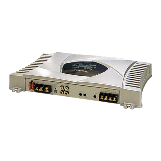
XM-D500X
2 9
8
SPECIFICATIONS
Q Q
3
6 7
1 3
1 5
Low-pass filter
Low boost
Power requirements
Power supply voltage
Current drain
Dimensions
Mass
Supplied accessories
Design and specifications are subject to change without
notice.
Notes on Chip Component Replacement
• Never reuse a disconnected chip component.
• Notice that the minus side of a tantalum capacitor may be
damaged by heat.
MONAURAL POWER AMPLIFIER
co
.
9 4
2 8
US Model
Canadian Model
AEP Model
UK Model
E Model
0 5
8
2 9
9 4
2 8
50 – 300 Hz, –12 dB/oct
0 – 10 dB (40 Hz)
12 V DC car battery
(negative ground)
10.5 – 16 V
at rated output : 50 A (at 2 Ω)
Remote input : 2 mA
Approx. 388 × 53 × 268 mm
(15
× 2
× 10
in.) (w/h/d) not incl.
3/8
1/8
1/8
projecting parts and controls
Approx. 3.3 kg (7 lb. 5 oz.) not incl. accessories
Mounting screws (4)
High level input cord (1)
Protection cap (1)
m
9 9
9 9
1
Advertisement
Table of Contents

Related Manuals for Sony XM-D500X


Summary of Contents for Sony XM-D500X
-
Page 1: Service Manual
• Never reuse a disconnected chip component. • Notice that the minus side of a tantalum capacitor may be damaged by heat. MONAURAL POWER AMPLIFIER u163 Sony Corporation 9-877-561-01 2004A04-1 e Vehicle Company © 2004. 01 Published by Sony Engineering Corporation http://www.xiaoyu163.com... -
Page 2: Table Of Contents
CRITIQUES POUR LA SÉCURITÉ DE FONCTIONNEMENT. NE REPLACE THESE COMPONENTS WITH SONY PARTS WHOSE REMPLACER CES COMPOSANTS QUE PAR DES PIÈCES SONY PART NUMBERS APPEAR AS SHOWN IN THIS MANUAL OR DONT LES NUMÉROS SONT DONNÉS DANS CE MANUEL OU IN SUPPLEMENTS PUBLISHED BY SONY. -
Page 3: General
XM-D500X SECTION 1 GENERAL 3 7 63 1515 0 This section is extracted from instruction manual. Location and Function Emplacement et of Controls fonction des commandes 1 POWER/PROTECTOR indicator Lights up in green during operation. 1 Indicateur POWER/PROTECTOR When the PROTECTOR is activated the indicator will change from green to red. -
Page 4: Connections
XM-D500X 3 7 63 1515 0 Connections Connexions Power Connection Wires Câbles d’alimentation Caution Attention • Before making any connections, disconnect • Avant d’effectuer les connexions, débranchez the ground terminal of the car battery to avoid la borne de masse de la batterie de voiture... -
Page 5: Input Connections
XM-D500X 3 7 63 1515 0 Input Connections Connexions d’entrée For details on the settings of switches and controls, refer to “Location and Function of Controls.” Pour plus de détails sur les réglages des commutateurs et commandes, reportez-vous à... - Page 6 — 2 – 8 Ω. • Do not connect any active speakers (with built-in In such a case, consult your nearest Sony dealer. possible qu’il y ait un dysfonctionnement interne. • Ne raccordez pas de haut-parleurs actifs (avec amplifiers) to the speaker terminals of the unit.
-
Page 7: Disassembly
XM-D500X SECTION 2 DISASSEMBLY 3 7 63 1515 0 Note : This set can be disassemble according to the following sequence. 2-1. BOTTOM PLATE (Page 7) 2-2. MAIN BOARD SECTION, LED BOARD (Page 8) 2-3. MAIN BOARD (Page 8) Note : Follow the disassembly procedure in the numerical order given. - Page 8 XM-D500X 3 7 63 1515 0 2-2. MAIN BOARD SECTION, LED BOARD 1 three screws (+BTP 3 x 14) 5 MAIN board section 2 three screws (+BTP 3 x 14) after unfastening the screw, taping with the screw inserted facilitates the wark.
-
Page 9: Diagrams
XM-D500X SECTION 3 DIAGRAMS 3 7 6 3 1 5 1 5 0 3-1. NOTE FOR PRINTED WIRING BOARD AND 3-2. IC BLOCK DIAGRAM • Semiconductor Location (Main Section) SCHEMATIC DIAGRAM Ref. No. Location Ref. No. Location IC6 TL494CN... - Page 10 XM-D500X 3 7 6 3 1 5 1 5 0 3-3. PRINTED WIRING BOARDS — MAIN SECTION — • Refer to page 9 for Semiconductor Location. MAIN BOARD (SIDE A) R118 R122 R116 R121 R153 C25 R137 R113 R143...
- Page 11 XM-D500X 3 7 6 3 1 5 1 5 0 MAIN BOARD (SIDE B) MC14 EC22 FET1 R101 E B C E B C DC-DC CONVERTER R124 TRANSFORMER R144 EC13 EC31 EC30 E B C E B C R145...
-
Page 12: Schematic Diagram -Main Section (1/2)
XM-D500X 3 7 6 3 1 5 1 5 0 3-4. SCHEMATIC DIAGRAM — MAIN SECTION (1/2) — CNT1 R136 R163 IC4(2/2) IC5(2/2) EC51 R164 IC5(1/2) IC2(2/2) IC2(1/2) R156 R169 EC17 IC4(1/2) R155 2.2k R174 EC52 IC3(1/2) IC3(2/2) MC10... -
Page 13: Schematic Diagram -Main Section (2/2)
XM-D500X 3 7 6 3 1 5 1 5 0 3-5. SCHEMATIC DIAGRAM — MAIN SECTION (2/2) — • Refer to page 9 for IC Block Diagram. R112 EC61 R114 R115 R110 R113 R143 R121 MC13 FET11 FET12 MC11... - Page 14 XM-D500X 3 7 6 3 1 5 1 5 0 MEMO 1 3 9 4 2 2 9 6 5 1 3 w w w u 1 6 3 http://www.xiaoyu163.com...
-
Page 15: Exploded Views
XM-D500X SECTION 4 EXPLODED VIEWS 3 7 63 1515 0 NOTE: • The mechanical parts with no reference • Color Indication of Appearance Parts The components identified by mark 0 or dotted line with mark number in the exploded views are not supplied. -
Page 16: Main Board Section
XM-D500X 3 7 63 1515 0 4-2. MAIN BOARD SECTION not supplied not supplied L 13942296513 Ref. No. Part No. Description Remark Ref. No. Part No. Description Remark A-3283-636-A MAIN BOARD, COMPLETE 3-253-537-01 SCREW (M5X11) u163 3-265-684-01 PANEL (FRONT) 3-912-431-01 SCREW (+–P) -
Page 17: Electrical Parts List
XM-D500X SECTION 5 MAIN ELECTRICAL PARTS LIST 3 7 63 1515 0 NOTE: • Due to standardization, replacements in • Items marked “*” are not stocked since The components identified by mark 0 or dotted line with mark the parts list may be different from the they are seldom required for routine service. - Page 18 XM-D500X MAIN 3 7 63 1515 0 Ref. No. Part No. Description Remark Ref. No. Part No. Description Remark 8-719-076-60 DIODE FCH20A15 < FUSE > 8-719-076-61 DIODE FRH20A15 8-719-989-91 DIODE 1N4148A-T265 0 FUSE1 1-533-743-11 FUSE (BLADE TYPE) (AUTO FUSE) (40A)
- Page 19 XM-D500X MAIN 3 7 63 1515 0 Ref. No. Part No. Description Remark Ref. No. Part No. Description Remark 8-729-034-50 TRANSISTOR KTA1504 1-216-825-11 METAL CHIP 2.2K 1/10W 8-729-034-51 TRANSISTOR KTC3875 1-216-825-11 METAL CHIP 2.2K 1/10W 8-729-034-51 TRANSISTOR KTC3875 1-216-837-11 METAL CHIP...
- Page 20 XM-D500X MAIN 3 7 63 1515 0 Ref. No. Part No. Description Remark Ref. No. Part No. Description Remark R102 1-216-206-00 RES-CHIP 2.2K 1/8W R166 1-216-833-11 METAL CHIP 1/10W R103 1-216-813-11 METAL CHIP 1/10W R167 1-216-825-11 METAL CHIP 2.2K...
- Page 21 XM-D500X 3 7 63 1515 0 Ref. No. Part No. Description Remark ACCESSORIES ************ 3-265-693-11 MANUAL, INSTRUCTION (ENGLISH,FRENCH) 3-265-693-21 MANUAL, INSTRUCTION (ITALIAN,GERMAN) (AEP,UK,E) 3-265-693-31 MANUAL, INSTRUCTION (SPANISH, TRADITIONAL CHINESE) (AEP,UK,E) 3-265-693-41 MANUAL, INSTRUCTION (PORTUGUESE,DUTCH) (AEP,UK,E) 3-265-693-51 MANUAL, INSTRUCTION (SWEDISH,POLISH)
- Page 22 XM-D500X 3 7 63 1515 0 REVISION HISTORY Clicking the version allows you to jump to the revised page. Also, clicking the version at the upper on the revised page allows you to jump to the next revised page.