
Related Manuals for Motorola GM Series


Summary of Contents for Motorola GM Series
- Page 1 Professional Radio GM Series VHF (136-174MHz) Service Information Issue: September 2000...
-
Page 2: Computer Software Copyrights
Accordingly, any copyrighted Motorola computer programs contained in the Motorola products described in this manual may not be copied or reproduced in any manner without the express written permission of Motorola. Furthermore, the purchase of Motorola... -
Page 3: Table Of Contents
Table of Contents Chapter 1 MODEL CHART AND TECHNICAL SPECIFICATIONS 1.0 GM140/GM160 Model Chart................1-1 2.0 GM340/GM360/GM380 Model Chart ..............1-1 3.0 GM640/GM660/GM1280 Model Chart ..............1-2 4.0 Technical Specifications ..................1-3 Chapter 2 THEORY OF OPERATION 1.0 Introduction ......................2-1 2.0 VHF (136-174MHz) Receiver................2-1 2.1 Receiver Front-End ..................2-1 2.1 Front-End Band-Pass Filters &... - Page 4 Chapter 3 TROUBLESHOOTING CHARTS 1.0 Troubleshooting Flow Chart for Receiver (Sheet 1 of 2) ........3-1 1.1 Troubleshooting Flow Chart for Receiver (Sheet 2 of 2) ........3-2 2.0 Troubleshooting Flow Chart for 25W Transmitter (Sheet 1 of 3) ......3-3 2.1 Troubleshooting Flow Chart for 25W Transmitter (Sheet 2 of 3) ......
-
Page 5: Model Chart And Technical Specifications
Chapter 1 MODEL CHART AND TECHNICAL SPECIFICATIONS GM140/GM160 Model Chart GM Series VHF 136-174 MHz Model Description MDM25KKC9AA1_E GM140, 136-174 MHz, 25-45W, 4 Ch MDM25KKF9AA5_E GM160, 136-174 MHz, 25-45W, 128 Ch Item Description GCN6112_ Control Head, GM140 GCN6114_ Control Head, GM160... -
Page 6: Gm340/Gm360/Gm380 Model Chart
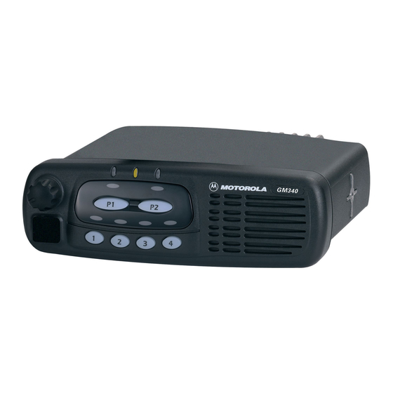
MODEL CHART AND TECHNICAL SPECIFICATIONS GM340/GM360/GM380 Model Chart GM Series VHF 136-174 MHz Model Description MDM25KHC9AN1_E GM340, 136-174 MHz, 1-25W, 6 Ch MDM25KHF9AN5_E GM360, 136-174 MHz, 1-25W, 255 Ch MDM25KHN9AN8_E GM380, 136-174 MHz, 1-25W, 255 Ch Item Description GCN6112_ Control Head GM340... -
Page 7: Gm640/Gm660/Gm1280 Model Chart
GM640/GM660/GM1280 Model Chart GM640/GM660/GM1280 Model Chart GM Series VHF 136-174 MHz Model Description MDM25KHC9CK1_E GM640, 136-174 MHz, 1-25W, 6 Ch MDM25KHF9CK5_E GM660, 136-174 MHz, 1-25W, 255 Ch MDM25KHN9CK8_E GM1280, 136-174 MHz, 1-25W, 255 Ch Item Description GCN6112_ Control Head GM640... -
Page 8: Technical Specifications
MODEL CHART AND TECHNICAL SPECIFICATIONS Technical Specifications Data is specified for +25°C unless otherwise stated. General Specifications Channel Capacity GM140 GM160 GM340 GM360 GM380 GM640 GM660 GM1280 Power Supply 13.2Vdc (10.8 - 15.6Vdc) Dimensions: H x W x D (mm) Depth excluding knobs GM140/340/640 56mm x 176mm x 177mm (1 - 25W) 56mm x 176mm x 189mm (25 - 45W) - Page 9 Technical Specifications Transmitter 136-174 *Frequencies - Full Bandsplit Channel Spacing 12.5/20/25 kHz Frequency Stability ±2.5 ppm (-30°C to +60°C, +25° Ref.) Power 1-25W / 25-45W ±2.5 @ 12.5 kHz Modulation Limiting ±4.0 @ 20 kHz ±5.0 @ 25 kHz -40 dB @ 12.5kHz FM Hum &...
- Page 10 MODEL CHART AND TECHNICAL SPECIFICATIONS...
-
Page 11: Theory Of Operation
Chapter 2 THEORY OF OPERATION Introduction This Chapter provides a detailed theory of operation for the VHF circuits in the radio. For details of the theory of operation and trouble shooting for the the associated Controller circuits refer to the Controller Section of this manual. -
Page 12: Front-End Band-Pass Filters & Pre-Amplifier
THEORY OF OPERATION There are two 2-pole 44.85 MHz crystal filters in the high-IF section and 2 pairs of 455 kHz ceramic filters in the low-IF section to provide the required adjacent channel selectivity. The correct pair of ceramic filters for 12.5 or 25kHz channel spacing is selected via control line BWSELECT. The second IF at 455 kHz is mixed, amplified and demodulated in the IF IC. -
Page 13: Vhf (136-174Mhz) Transmitter Power Amplifier (Pa) 25 W
VHF (136-174MHz) Transmitter Power Amplifier (PA) 25 W low IF signal is amplified and filtered by an external pair of 455 kHz ceramic filters FL3112, FL3114 for 20/25 kHz channel spacing or FL3111, FL3113/F3115 for 12.5 kHz channel spacing. These pairs are selectable via BWSELECT. -
Page 14: Power Controlled Driver Stage
THEORY OF OPERATION Op-amp U3402-1 monitors the drain current of U3401 via resistor R3444 and adjusts the bias voltage of U3401 so that the current remains constant. The PCIC (U3501) provides a DC output voltage at pin 4 (INT) which sets the reference voltage of the current control loop. A raising power output causes the DC voltage from the PCIC to fall, and U3402-1 adjusts the bias voltage for a lower drain current to lower the gain of the stage. -
Page 15: Antenna Switch
VHF (136-174MHz) Transmitter Power Amplifier (PA) 25 W Antenna Switch The antenna switch consists of two PIN diodes, D3471 and D3472. In the receive mode, both diodes are off. Signals applied at the antenna jack J3401 are routed, via the harmonic filter, through network L3472, C3474 and C3475, to the receiver input. -
Page 16: Vhf (136-174Mhz) Frequency Synthesis
THEORY OF OPERATION VHF (136-174MHz) Frequency Synthesis The frequency synthesizer subsystem consists of the reference oscillator (Y3261 or Y3263), the Low Voltage Fractional-N synthesizer (LVFRAC-N, U3201), and the voltage-controlled oscillators and buffer amplifiers (U3301, Q3301-2 and associated circuitry). Reference Oscillator The reference oscillator (Y3263) contains a temperature compensated crystal oscillator with a frequency of 16.8 MHz. -
Page 17: Voltage Controlled Oscillator (Vco)
VHF (136-174MHz) Frequency Synthesis A voltage of 5V applied to the super filter input (U3201 pin 30) supplies an output voltage of 4.5 VDC (VSF) at pin 28. It supplies the VCO, VCO modulation bias circuit (via R3363) and the synthesizer charge pump resistor network (R3251, R3252). -
Page 18: Synthesizer Operation
THEORY OF OPERATION The VCOBIC together with the Fractional-N synthesizer (U3201) generates the required frequencies in both the transmit and receive modes. The TRB line (U3301 pin 19) determines which tank circuits and internal buffers are to be enabled. A high level on TRB enables the TX tank and TX output (pin 10), and a low enables the RX tank and RX output (pin 8). -
Page 19: Vhf (136-174Mhz) Transmitter Power Amplifier (Pa) 45 W
VHF (136-174MHz) Transmitter Power Amplifier (PA) 45 W signal into a digital code that is applied to the loop divider, thereby causing the carrier to deviate. The balance attenuator is used to adjust the VCO’s deviation sensitivity to high frequency modulating signals. -
Page 20: Pre-Driver Stage
2-10 THEORY OF OPERATION Pre-Driver Stage The next stage is an LDMOS device (Q3421) providing a gain of 13 dB. This device requires a positive gate bias and a quiescent current flow for proper operation. The voltage of the line PCIC_MOSBIAS_1 is set during transmit mode by the PCIC pin 24, and fed to the gate of Q3421 via the resistive network R3410, R3415, and R3416. -
Page 21: Antenna Switch
VHF (136-174MHz) Transmitter Power Amplifier (PA) 45 W 2-11 Antenna Switch The antenna switch consists of two PIN diodes, D3471 and D3472. In the receive mode, both diodes are off. Signals applied at the antenna jack J3401 are routed, via the harmonic filter, through network L3472, C3474 and C3475, to the receiver input. - Page 22 2-12 THEORY OF OPERATION...
-
Page 23: Troubleshooting Charts
Chapter 3 TROUBLESHOOTING CHARTS Troubleshooting Flow Chart for Receiver (Sheet 1 of 2) START Bad SINAD Bad 20dB Quieting No Recovered Audio Check Controller Audio at (in the case of no audio) pin 8 of OR ELSE go to “B” U3101 ? Spray or inject 44.85MHz into XTAL Filter FL3101... -
Page 24: Troubleshooting Flow Chart For Receiver (Sheet 2 Of 2)
TROUBLESHOOTING CHARTS Troubleshooting Flow Chart for Receiver (Sheet 2 of 2) Inject RF into J3401 Trace IF signal from C3035 to Q3101. IF Signal at Check for bad XTAL IF signal at Q3102 C3035? filter collector? Before replacing U3101, check U3101 voltages RF Signal at LO level OK? -
Page 25: Troubleshooting Flow Chart For 25W Transmitter (Sheet 1 Of 3)
Troubleshooting Flow Chart for 25W Transmitter (Sheet 1 of 3) Troubleshooting Flow Chart for 25W Transmitter (Sheet 1 of 3) START No or too low Power when keyed Check if Pressure Pad closes S3440 Check Components between Current Q3441 and RF Output, >500mA &... -
Page 26: Troubleshooting Flow Chart For 25W Transmitter (Sheet 2 Of 3)
TROUBLESHOOTING CHARTS Troubleshooting Flow Chart for 25W Transmitter (Sheet 2 of 3) Check PA Stages No or too low Power when keyed DC Voltage If U3201 Pin 2 is high, at U3501 replace PCIC Pin 23 =0? Check Resistive Net- >6 <2V Voltage at... -
Page 27: Troubleshooting Flow Chart For 25W Transmitter (Sheet 3 Of 3)
Troubleshooting Flow Chart for 25W Transmitter (Sheet 1 of 3) Troubleshooting Flow Chart for 25W Transmitter (Sheet 3 of 3 Check Final PA Stage Supply Voltage Bias 2 DC Voltage at Replace Q3441 TP3406? 1-4V Check Components ASFIC RF Voltage between ASFIC and U0221 Pin 6 Check FGU (U3301) -
Page 28: Troubleshooting Flow Chart For 45W Transmitter (Sheet 1 Of 2)
TROUBLESHOOTING CHARTS Troubleshooting Flow Chart for 45W Transmitter (Sheet 1 of 2) START No or too low Power when keyed Current in- Check Components between >500mA & <5A >5A crease when Q3441 and RF Output, Antenna keyed? Switch D3471,D3472 <500mA Control Voltage at Check PA Stages... - Page 29 Troubleshooting Flow Chart for 45W Transmitter (Sheet 1 of 2) Troubleshooting Flow Chart for Transmitter (Sheet 2 of 2) Check PA Stages No or too low Power when keyed Pin 3 Voltage 0.51 Check Voltage at Pin 2 & 3 of U3401 Replace U3401 * Voltage at Pin 1?
-
Page 30: Troubleshooting Flow Chart For Synthesizer
TROUBLESHOOTING CHARTS Troubleshooting Flow Chart for Synthesizer 5V at Check 5V U3201 pins 5, Start Regulator 20, 34 & 36 U3211, R3211 Visual Correct check of the Problem Board OK? Is 16.8MHz 16.8MHz Replace Signal at signal at U3201 Is U3201 U3201 Pin U3201 pin at pin 6 of... -
Page 31: Troubleshooting Flow Chart For Vco
Troubleshooting Flow Chart for VCO Troubleshooting Flow Chart for VCO Low or no RF Signal Low or no RF Signal TX VCO RX VCO at input to PA at TP3001 Visual check Visual check Correct of board of board Problem Make sure U3211 is working correctly and runner 5V DC at U3301... - Page 32 3-10 TROUBLESHOOTING CHARTS...
-
Page 33: Allocation Of Schematics And Circuit Boards
Chapter 4 VHF PCB/SCHEMATICS/PARTS LISTS Allocation of Schematics and Circuit Boards Controller Circuits The VHF circuits are contained on the printed circuit board (PCB) which also contains the Controller circuits. This Chapter shows the schematics for the VHF circuits only, refer to the Controller section for details of the related Controller circuits . - Page 34 VHF PCB/SCHEMATICS/PARTS LISTS Table 4-3 VHF 1-25W Diagrams and Parts Lists PCB : 8486172B07 Main Board Top Side Page 4-23 8486172B07 Main Board Bottom Side Page 4-24 SCHEMATICS Power Amplifier 1 - 25W Page 4-15 Voltage Controlled Oscillator Page 4-17 Receiver Front End Page 4-18 Page 4-25...