Table of Contents
Advertisement
SERVICE MANUAL
Ver 1.1 2001.02
With SUPPLEMENT-1
(9-928-809-81)
Note
CD block, tape deck block and
tuner pack are supplied with
the assembled block.
HCD-CP1 is the Amplifier, CD player,
Tape Deck and Tuner section in
CMT-CP1.
Dolby noise reduction manufactured under license
from Dolby Laboratories Licensing Corporation.
"DOLBY" and the double-D symbol a are trade-
marks of Dolby Laboratories Licensing Corporation.
Sony Corporation
9-928-809-12
2001B0500-1
Audio Entertainment Group
C 2001.2
General Engineering Dept.
HCD-CP1
Model Name Using Similar Mechanism
CD
CD Mechanism Type
Section
Optical Pick-up Name
Model Name Using Similar Mechanism
Tape deck
Section
Tape Transport Mechanism Type
SPECIFICATIONS
MICRO HiFi COMPONENT SYSTEM
US Model
Canadian Model
AEP Model
UK Model
E Model
Australian Model
NEW
KSL-2130CCP/K1N
KSS-213C/K1N
HCD-ED1
CMAL1Z023A
– Continued on next page –
Advertisement
Table of Contents

Related Manuals for Sony HCD-CP1


Summary of Contents for Sony HCD-CP1
- Page 1 Australian Model CD block, tape deck block and tuner pack are supplied with the assembled block. HCD-CP1 is the Amplifier, CD player, Tape Deck and Tuner section in CMT-CP1. Dolby noise reduction manufactured under license Model Name Using Similar Mechanism from Dolby Laboratories Licensing Corporation.
- Page 2 – 2 –...
-
Page 3: Table Of Contents
SECTION 1 SERVICING NOTES TABLE OF CONTENTS SERVICING NOTES ..........3 NOTES ON HANDLING THE OPTICAL PICK-UP BLOCK OR BASE UNIT GENERAL The laser diode in the optical pick-up block may suffer electro- Location of Controls ............5 static break-down because of the potential difference generated Setting the Time .............. - Page 4 SUR LES DIAGRAMMES SCHÉMATIQUES ET LA LISTE DES PIÈCES SONT CRITIQUES POUR LA SÉCURITÉ DE FONCTIONNEMENT. NE REMPLACER CES COM- VOLTAGE SELECTOR POSANTS QUE PAR DES PIÈCES SONY DONT LES Switch NUMÉROS SONT DONNÉS DANS CE MANUEL OU DANS LES SUPPLÉMENTS PUBLIÉS PAR SONY.
-
Page 5: General
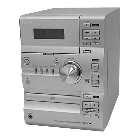
SECTION 2 GENERAL LOCATION OF CONTROLS • Front View 1 2 3 4 5 6 TAPE deck Liquid crystal display TAPE P button TAPE 0 button TAPE œ button TAPE 6 button TAPE p button !º !ª TAPE ) button @º... - Page 6 This section is extracted from instruction manual. – 6 –...
-
Page 7: Disassembly
SECTION 3 DISASSEMBLY Note: Follow the disassembly procedure in the numerical order given. COVER (UPPER) 3 cover (upper) 2 four screws (BTP3 × 8) 1 two screws (case3 TP2) 1 two screws (case3 TP2) TAPE MECHANISM DECK 1 flat wire (12 core) 4 tape mechanism deck 3 two screws... - Page 8 FRONT PANEL SECTION 2 two flat wires (CN802, 804) 1 connector (CN303) 1 connector 2 flat wire (12 core) 1 connector (CN809) 3 screw (KTP3 × 6) 6 connector (CN603) 5 two claws 7 front panel section 3 screw 4 two screws (KTP3 ×...
- Page 9 CD MECHANISM DECK 3 two screws (BTP3 × 8) 2 flat wire (19 core) (CN805) 3 two screws (BTP3 × 8) 1 connector 4 CD mechanism deck BU ASS’Y Note: As 3 coil springs are missed easily, treat them carefully. 3 coil spring (rear) 2 washer...
- Page 10 TRAY 1 two screws (PTPWH2.6 × 7) 2 chucking yoke (K) 6 damper (S) 7 lock lever 4 Pull the tray. 8 Remove the tray. 5 claw 7 lock lever 3 Rotate the control cam in the direction of arrow A . •...
-
Page 11: Service Mode
SECTION 4 SERVICE MODE [Liquid Crystal Display All Lit Check Mode] [CD Aging Mode] This mode can be used for operation check of CD section. Procedure: 1. Set to standby state. Procedure: [MD/VIDEO] 2. Press three buttons of p (TAPE), p (CD), and 1. -
Page 12: Electrical Confirmations And Adjustments
SECTION 5 ELECTRICAL CONFIRMATIONS AND ADJUSTMENTS 2. Turn the adjustment screw and check output peaks. If the peaks DECK SECTION 0 dB=0.775 V do not match for L-CH and R-CH, turn the adjustment screw Note: Confirm each contents of this section first of all. If the results are so that outputs match within 1dB of peak. - Page 13 REC Level Confirmation and Adjustment Playback level Confirmation and Adjustment Procedure: Procedure: 1. Mode: Record Mode: Playback MAIN board test tape MD IN jack (PJ301) WS-48B L-CH, R-CH frequency counter (3 kHz, 0 dB) 315 Hz, 50 mV (–23.8 dB) AF OSC blank tape 600 Ω...
-
Page 14: Diagrams
HCD-CP1 SECTION 6 DIAGRAMS 6-1. BLOCK DIAGRAM – TAPE Section – REC-L (Page 18) DECK PROCESS, RV151 DOLBY NR AMP PLAYBACK IC352 LEVEL (L) DECK A/B PB-L PLAYBACK SELECT DOLBY NR (Page 17) EQ AMP L-CH IC351 CIRCUIT REC/PB REC/PB... -
Page 15: Block Diagram - Main Section
HCD-CP1 6-2. BLOCK DIAGRAM – MAIN Section – REC-L PB-L (Page 16) (Page 16) PJ301 (1/2) INPUT SELECT SWITCH, TONE CONTROL, ELECTRICAL VOLUME MD IN IC301 LINE AMP R-CH PJ301 (2/2) IC307 LINE OUT LIN2 MUTING R-CH Q101 LIN1 VIDEO IN... -
Page 16: Block Diagram - Display/Power Supply Section
HCD-CP1 6-3. BLOCK DIAGRAM – DISPLAY/POWER SUPPLY Section – REC/PB SYSTEM CONTROLLER, D801, 802 (Page 16) BACK UP +5V LCD DRIVER SYSTEM CONTROLLER (IC801) B+ IC801 (3/3) RESET SIGNAL RESET 38 GENERATOR (EXCEPT Hong Kong, Malaysia, Singapore, Thai) IC803 POWER TRANSFORMER... - Page 17 6-4. NOTE FOR PRINTED WIRING BOARDS AND SCHEMATIC DIAGARAMS • Circuit Boards Location Note on Printed Wiring Board: Note on Schematic Diagram: POWER board • X : parts extracted from the component side. • All capacitors are in µF unless otherwise noted. pF: µµF •...
-
Page 18: Printed Wiring Board - Main Section
HCD-CP1 6-5. PRINTED WIRING BOARD – MAIN Section – • See page 22 for Circuit Boards Location. (Page 33) (Page 33) (Page 37) (Page 33) (Page 33) (Page 41) – 23 – – 24 –... -
Page 19: Schematic Diagram – Main Section (1/4)
HCD-CP1 • Voltages and waveforms are dc with respect to ground under no-signal (detuned) conditions. no mark : FM ) : CD PLAY 6-6. SCHEMATIC DIAGRAM – MAIN Section (1/4) – • See page 35 for IC Block Diagram. ] : TAPE PLAY 〈〈... -
Page 20: Schematic Diagram - Main Section (1/4)
HCD-CP1 6-7. SCHEMATIC DIAGRAM – MAIN Section (2/4) – • See page 35 for IC Block Diagrams. (Page 42) (Page (Page 31) (Page 32) • Voltages and waveforms are dc with respect to ground under no-signal (detuned) conditions. no mark : FM... -
Page 21: Schematic Diagram – Main Section (3/4)
HCD-CP1 6-8. SCHEMATIC DIAGRAM – MAIN Section (3/4) – • See page 34 for Waveforms. (Page 25) (Page 31) (Page 32) • Voltages and waveforms are dc with respect to ground under no-signal conditions. no mark : TAPE PLAY ) : TAPE RECORD –... -
Page 22: Schematic Diagram - Main Section (2/4)
HCD-CP1 6-9. SCHEMATIC DIAGRAM – MAIN Section (4/4) – • See page 34 for Waveforms. • See page 36 for IC Block Diagram. (Page 39) (Page 30) (Page 28) (Page 30) (Page 25) (Page 28) (Page 25) (Page 25) • Voltages and waveforms are dc with respect to ground under no-signal (detuned) conditions. -
Page 23: Printed Wiring Boards - Panel/Cd Loading Section
HCD-CP1 6-10. PRINTED WIRING BOARDS – PANEL/CD LOADING Section – • Waveforms – MAIN Board – • See page 22 for Circuit Boards Location. 4 IC804 !§ (RCLK) 1 Q357, 358 collector (REC mode) 13.6 Vp-p 4.4 Vp-p 11.6 µ s 840 µ... - Page 24 • IC Block Diagrams IC804 BU1924F-E2 (AEP, UK models) – MAIN Board – IC101, 201 TDA7296 12 11 10 THERMAL BIPOLAR SHUTDOWN TRANSCONDACTANCE INPUT STAGE CLOCK TEST MOS GAIN & SHORT – LEVEL SHIFTING OUTPUT CIRCUIT STAGE STAGE PROTECTION PLL 57kHz RDS/ARI 1187.5Hz COMPARATOR...
-
Page 25: Printed Wiring Boards - Control Section
HCD-CP1 6-11. PRINTED WIRING BOARDS – CONTROL Section – • See page 22 for Circuit Boards Location. (Page 23) • Semiconductor Location Ref. No. Location D851 D852 D853 D854 D855 D856 D857 IC802 Q852 Q853 Q854 Q855 Q856 Q857 Q858 Q859 –... -
Page 26: Schematic Diagram - Control Section
HCD-CP1 6-12. SCHEMATIC DIAGRAM – CONTROL Section – (Page 32) • Voltages and waveforms are dc with respect to ground under no-signal (detuned) conditions. no mark : FM – 39 – – 40 –... -
Page 27: Printed Wiring Board - Power Section
HCD-CP1 6-13. PRINTED WIRING BOARD – POWER Section – 6-14. SCHEMATIC DIAGRAM – POWER Section – • See page 22 for Circuit Boards Location. (Page (Page 23) The components identified by mark ! or dotted Les composants identifiés par une marque ! sont line with mark ! are critical for safety. -
Page 28: Ic Pin Function Description
6-15. IC PIN FUNCTION DESCRIPTION • MAIN BOARD IC801 CXP83124A-130Q (SYSTEM CONTROLLER, LCD DRIVER) Pin No. Pin Name Description TAPE-END Tape end detect sensor input terminal “H” input when the tape end detected Serial data reading clock signal input from the RDS decoder (IC804) RDS-CLK (Used for the AEP and UK models only) REMOCON... - Page 29 Pin No. Pin Name Description Power supply on/off control signal output of the tuner pack (+7.5V) and RDS decoder (IC804) RDS-ON (RDS decoder: used for the AEP and UK models only) LED drive signal output of the TUNER indicator (D855) “H”: tuner power on (LED on) HP-CHK Headphone check detection signal input terminal TC-SW...
-
Page 30: Exploded Views
SECTION 7 EXPLODED VIEWS NOTE: • -XX and -X mean standardized parts, so they • Items marked “*” are not stocked since they The components identified by mark ! or dotted line with mark may have some difference from the original are seldom required for routine service. - Page 31 (2) FRONT PANEL SECTION supplied supplied with RV801 supplied Ref. No. Part No. Description Remark Ref. No. Part No. Description Remark X-4951-108-1 KNOB ASSY * 62 4-217-320-01 PLATE, BACK LIGHT X-4951-102-1 PANEL SUB ASSY, FRONT (AEP, UK) (CASSETTE HOLDER BACK LIGHT) X-4951-702-1 PANEL SUB ASSY, FRONT (EXCEPT AEP, UK) X-4951-107-1 LOCK (EJECT) ASSY 4-217-318-01 WINDOW (CASSETTE)
- Page 32 (3) CHASSIS SECTION US, CND AEP, MY, UK, HK SP, TH KSL-2130CCP/K1N T901 supplied 103 114 supplied supplied supplied supplied The components identified by Les composants identifiés par une mark ! or dotted line with marque ! sont critiques pour la mark ! are critical for safety.
- Page 33 HCD-CP1 Ver 1.1 2001.02 (4) CD MECHANISM DECK SECTION (KSL-2130CCP/K1N) supplied supplied supplied supplied M901 Ref. No. Part No. Description Remark Ref. No. Part No. Description Remark * 151 2-646-290-01 TRAY (2130) 1-452-493-21 MAGNET 2-167-349-01 PIN (RP), TRAY 2-625-286-03 PULLEY, CHUKING 2-625-279-01 SCREW (B 2.6X2.5), +...
-
Page 34: Electrical Parts List
SECTION 8 CD LIGHT CONTROL ELECTRICAL PARTS LIST NOTE: • Due to standardization, replacements in the • Items marked “*” are not stocked since they The components identified by mark ! or dotted line with mark are seldom required for routine service. parts list may be different from the parts speci- ! are critical for safety. - Page 35 CONTROL LOADING MAIN Ref. No. Part No. Description Remark Ref. No. Part No. Description Remark S802 1-571-760-11 SWITCH, KEY BOARD (CD, ^) < LED > S803 1-571-760-11 SWITCH, KEY BOARD (CD, p) S804 1-571-760-11 SWITCH, KEY BOARD (CD, + )) D657 8-719-075-51 LED SELS6B14C-LF62 (LCD BACK LIGHT) S805...
- Page 36 MAIN Ref. No. Part No. Description Remark Ref. No. Part No. Description Remark C126 1-126-965-11 ELECT 22uF C254 1-104-666-11 ELECT 220uF C127 1-130-495-00 MYLAR 0.1uF C255 1-163-117-00 CERAMIC CHIP 100PF C256 1-130-487-00 MYLAR 0.022uF C128 1-163-005-11 CERAMIC CHIP 470PF C257 1-124-907-11 ELECT 10uF C129...
- Page 37 MAIN Ref. No. Part No. Description Remark Ref. No. Part No. Description Remark C363 1-163-021-11 CERAMIC CHIP 0.01uF C364 1-124-907-11 ELECT 10uF D361 8-719-991-33 DIODE 1SS133T-77 D362 8-719-991-33 DIODE 1SS133T-77 C365 1-163-021-11 CERAMIC CHIP 0.01uF D651 8-719-200-82 DIODE 11ES2 C603 1-164-004-11 CERAMIC CHIP 0.1uF D652...
- Page 38 MAIN Ref. No. Part No. Description Remark Ref. No. Part No. Description Remark JR325 1-216-296-00 SHORT Q658 8-729-900-53 TRANSISTOR DTC114EK JR326 1-216-296-00 SHORT JR327 1-216-296-00 SHORT Q659 8-729-900-53 TRANSISTOR DTC114EK JR328 1-216-296-00 SHORT Q661 8-729-040-76 TRANSISTOR KTA1273-Y-AT Q662 8-729-900-53 TRANSISTOR DTC114EK <...
- Page 39 MAIN Ref. No. Part No. Description Remark Ref. No. Part No. Description Remark R157 1-216-065-00 RES, CHIP 4.7K 1/10W R309 1-216-041-00 METAL CHIP 1/10W R158 1-216-061-00 METAL CHIP 3.3K 1/10W R310 1-216-073-00 METAL CHIP 1/10W R159 1-216-049-11 RES, CHIP 1/10W R311 1-216-073-00 METAL CHIP 1/10W...
- Page 40 MAIN Ref. No. Part No. Description Remark Ref. No. Part No. Description Remark R670 1-216-097-00 RES, CHIP 100K 1/10W R844 1-216-089-00 RES, CHIP 1/10W (AEP, UK) R846 1-216-081-00 METAL CHIP 1/10W R671 1-216-113-00 RES, CHIP 470K 1/10W R847 1-216-073-00 METAL CHIP 1/10W (AEP, UK) R848...
- Page 41 MAIN POWER Ref. No. Part No. Description Remark Ref. No. Part No. Description Remark RV251 1-241-765-11 RES, ADJ, CARBON 22K D911 8-719-046-07 DIODE 2A02M RV252 1-225-231-21 RES, ADJ, CARBON 4.7K D912 8-719-046-07 DIODE 2A02M RV253 1-241-767-21 RES, ADJ, CARBON 100K D913 8-719-046-07 DIODE 2A02M D914...
- Page 42 Ref. No. Part No. Description Remark Ref. No. Part No. Description Remark ************** HARDWARE LIST ************** 7-685-546-14 SCREW +BTP 3X8 TYPE2 N-S 7-685-245-19 SCREW +KTP 3X6 TYPE2 NON-SLIT 7-685-246-14 SCREW +KTP 3X8 TYPE2 NON-SLIT 7-685-659-14 SCREW +BVTP 4X8 TYPE2 N-S (EXCEPT AEP, UK) 7-685-659-79 SCREW +BVTP 4X8 TYPE2 IT-3 (AEP, UK) 7-685-135-19 SCREW +P 2.6X10 TEPE2 NON-SLIT...
- Page 43 HCD-CP1 Ref. No. Part No. Description Remark Ref. No. Part No. Description Remark Sony Corporation 99B0589-1 Printed in Japan © 1999. 2 9-928-809-11 Home A&V Products Company Published by Quality Assurance Dept. – 58 – (Shinagawa)
- Page 44 HCD-CP1 US Model Canadian Model SERVICE MANUAL AEP Model UK Model E Model 2000.11 Australian Model SUPPLEMENT-1 File this supplement with the service manual. Subject: 1. Addition of E, Saudi Arabia, Taiwan, Mexican, Argentine and Australian Models 2. CD Test Mode 1.
- Page 45 1-2. Diagrams : Indicates changed portion. Page Before Change After Change [MAIN BOARD] Location: G-4 EXCEPT US, CND, AEP, UK [MAIN BOARD] (2/4) Location: D-5 R124, 224 2.2k (E, MX, AR) 22k (EXCEPT E, MX, AR) [MAIN BOARD] (2/4) Location: H-9 EXCEPT US, CND, AEP, UK [MAIN BOARD] (4/4) Location: E-13...
- Page 46 : Indicates changed portion. Page Before Change After Change [POWER BOARD] EXCEPT US, CND, AEP, UK US, CND, AEP, UK, TH, MX, AUS [POWER BOARD] Location: B-D, 5-6 E, EA ,MY, SP, HK, TW, AR The components identified by Les composants identifiés par une mark 0 or dotted line with marque 0 sont critiques pour la mark 0 are critical for safety.
- Page 47 1-3. Exploded Views • Abbreviation AR : Argentine model MX : Mexican model AUS : Australian model MY : Malaysia model CND : Canadian model : Singapore model EA : Saudi Arabia model TH : Thai model HK : Hong Kong model TW : Taiwan model : Indicates changed portion.
- Page 48 : Indicates changed portion. Page Before Change After Change Ref. No. Part No. Description Remark Ref. No. Part No. Description Remark 2-625-541-02 DAMPER (S) 2-167-349-01 PIN (RP), TRAY 3-635-387-00 BELT, LM 3-653-387-00 BELT, LM 2-625-285-04 GEAR, DRIVE 2-625-283-05 CAM, CONTROL supplied supplied supplied...
- Page 49 1-4. Electrical Parts List • Abbreviation AR : Argentine model HK : Hong Kong model TH : Thai model AUS : Australian model MX : Mexican model TW : Taiwan model CND : Canadian model MY : Malaysia model EA : Saudi Arabia model : Singapore model Page Before Change...
-
Page 50: Cd Test Mode
2. CD Test Mode 2. STOP Mode [EJECT ] 1. Press the button twice to disc tray open and close. (All servo ON) In the CD test mode, the set works as following sequence. 2. Press the button to move the optical pick-up >... - Page 51 HCD-CP1 4. ALL SERVO ON Mode Connecting Location: 1. Press the button to enter the ALL SERVO ON mode and – BD BOARD (Conductor Side) – display as below. (All servo ON) Display STEREO * * * * 2. Connect an oscilloscope to TP (RF) and TP (VC) on the BD board.
- Page 52 HCD-CP1 MEMO...
-
Page 53: Revision History
HCD-CP1 REVISION HISTORY Clicking the version allows you to jump to the revised page. Also, clicking the version at the upper right on the revised page allows you to jump to the next revised page. Ver. Date Description of Revision 2001.02...