Table of Contents
Advertisement
SERVICE MANUAL
Ver 1.5 2004.09
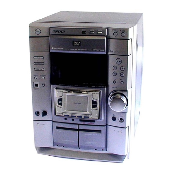
• HCD-DP900D is the tuner, deck,
DVD and amplifier section in MHC-
DP900D.
Amplifier section
The following measured at AC 120, 220, 240 V,
50/60 Hz
DIN power output (rated) 130 + 130 watts
(6 ohms at 1 kHz, DIN)
Continuous RMS power output (reference)
180 + 180 watts
(6 ohms at 1 kHz, 10% THD)
Inputs
GAME IN:
voltage 250 mV,
(phono jacks)
impedance 47 kilohms
MD (VIDEO) IN:
voltage 450 mV/250 mV,
(phono jacks)
impedance 47 kilohms
OPTICAL IN:
(Square optical connector jacks, front panel)
wavelength
——
MIC:
sensitivity 1 mV,
(Except for North
impedance 10 kilohms
American and
European models)
(phone jack)
Sony Corporation
9-873-312-06
Audio Group
2004I02-1
Published by Sony Engineering Corporation
© 2004.09
HCD-DP900D
Model Name Using Similar Mechanism
DVD
DVD Mechanism Type
Section
Base Unit Name
Optical Pick-up Name
Tape deck
Model Name Using Similar Mechanism
Section
Tape Transport Mechanism Type
SPECIFICATIONS
Outputs
MD (VIDEO) OUT:
(phono jacks)
VIDEO OUT:
(phono jack)
S-VIDEO OUT: Y:
(4-pin/mini-DIN jack)
PHONES:
(stereo mini jack)
SPEAKER:
SUB WOOFER:
MINI HI-FI COMPONENT SYSTEM
E Model
NEW
CDM58D-DVBU9
DVBU9
KHM-240AAA/CLNP
HCD-DP800AV
TCM-230AWR41/MWR41
voltage 250 mV
impedance 1 kilohms
max. output level
1 Vp-p, unbalanced, Sync
negative, load impedance
75 ohms
1 Vp-p, unbalanced,
Sync negative,
C: 0.286Vp-p,
load impedance 75 ohms
accepts headphones of
8 ohms or more
accepts impedance of 6 to
16 ohms
Voltage 1 V,
impedance 1 kilohms
— Continued on next page —
Advertisement
Table of Contents

Related Manuals for Sony HCD-DP900D


Summary of Contents for Sony HCD-DP900D
- Page 1 HCD-DP900D SERVICE MANUAL E Model Ver 1.5 2004.09 • HCD-DP900D is the tuner, deck, DVD and amplifier section in MHC- DP900D. Model Name Using Similar Mechanism DVD Mechanism Type CDM58D-DVBU9 Section Base Unit Name DVBU9 Optical Pick-up Name KHM-240AAA/CLNP Tape deck...
- Page 2 CD: λ =780 nm) MARK 0 ON THE SCHEMATIC DIAGRAMS AND IN THE PARTS LIST ARE CRITICAL TO SAFE OPERATION. REPLACE THESE Emission duration: COMPONENTS WITH SONY PARTS WHOSE PART NUMBERS continuous Frequency response DVD (PCM 48 kHz): APPEAR AS SHOWN IN THIS MANUAL OR IN SUPPLEMENTS 2 Hz –...
-
Page 3: Table Of Contents
,Re-insert the disc correctly. To prevent a malfunction, the E XX system has performed the self-diagnosis (XX is a number) function. ,Contact your nearest Sony dealer or local authorized Sony service facility and give the 5-character service number. Example: E 61 10... - Page 4 HCD-DP900D Ver 1.5 SERVICE POSITION • DISC TRAY LOCK The disc tray lock function for the antitheft of an demonstration disc in the store is equipped. Releasing Procedure : Press three buttons of PLAY MODE , x and m simultaneously.
-
Page 5: General
HCD-DP900D SECTION 1 Ver 1.2 2002.07 GENERAL This section is extracted from instruction manual. Parts Identification The items are arranged in alphabetical order. Main unit ea esedefegeh rgrf rdrs 2CH/MULTI rs (24, 46) MIC LEVEL control (Except for Setting the time... -
Page 6: Disassemby
HCD-DP900D SECTION 2 DISASSEMBLY • The equipment can be removed using the following procedure. Case (Top) Loading Panel Front Panel Section Tape Mechanism Deck LEAF SW board, Head (A) board, (TCM-230AWR41/MWR41) Head (B) board Escutcheon pad CD Panel board, Panel board, OPT IN Board... - Page 7 HCD-DP900D 2-2. LOADING PANEL 4 pull-out the disc tray. DVD mechanism deck (CDM58D) 1 turn the pulley to the direction of arrow. loading panel front panel side pulley 2 pull-out the disc tray. 2-3. FRONT PANEL SECTION, DVD MECHANISM DECK (CDM58D) qa connector (CN204) qg three screws (+BVTP 3 ×...
- Page 8 HCD-DP900D 2-4. TAPE MECHANISM DECK (TCM-230AWR41/MWR41) 1 four screws (+BVTP 2.6 × 8) 2 tape mechanism deck (TCM-230AWR41/MWR41) 2-5. CD PANEL BOARD, PANEL BOARD, OPT IN BOARD 1 five screws (+BVTP 2.6 × 8) two claws qf flat type wire (CN108)
- Page 9 HCD-DP900D 2-6. ESCUTCHEON PAD (WITH TOUCH PAD) 1 button (edit) 6 two screws (TPG +P 2 × 8) 8 three screws 3 two screws (+BVTP 2.6 × 8) (+BVTP 2.6 × 8) 9 button (DSP) 2 two screws (+BVTP 2.6 × 8) 5 two screws (TPG +P 2 ×...
- Page 10 HCD-DP900D 2-8. TRANS BOARD, MAIN BOARD 4 two screws 8 two screws 6 TRANS board (+BVTP 3 × 8) (+BVTT 4 × 8) 5 two screws 7 two screws (+BVTT 4 × 8) (+BVTT 3 × 8) 1 connector (CN914) 0 t wo screws (+BVTP 3 ×...
- Page 11 HCD-DP900D 2-10. LEAF SW BOARD, HEAD (A) BOARD, HEAD (B) BOARD (TCM-230AWR41/MWR41) Note: This illustration is for TCM-230MWR, but in case of TCM-230AWR, you can remove them in the same way. 1 five claws 2 LEAF SW board 3 remove the four solderings.
- Page 12 HCD-DP900D 2-12. RF-240 BOARD, OPTICAL PICK-UP (KHM-240AAA) qd optical pick-up (KHM-240AAA) 7 step screw (L) 0 insulator 9 step screw (10) 5 flat type wire (26 core) 6 flat type wire (9 core) qs insulator 8 step screw (10) qa insulator 4 holder (DVD) assy 3 floating screw (+PTPWHM2.6)
-
Page 13: Test Mode
HCD-DP900D SECTION 3 TEST MODE [Cold Reset] [MC Test Mode] • The cold reset clears all data including preset data stored in the • This mode is used to check operations of the respective sections RAM to initial conditions. Execute this mode when returning of Amplifier, Tuner, and Tape. - Page 14 HCD-DP900D [Aging Mode] This mode can for operation check of tape deck section and DVD section. • If an error occurred: The aging operation stops and display then status. • If no error occurs: The aging operation continues repeatedly. Procedure: 1.
- Page 15 HCD-DP900D [DVD Section] 2. CDM Error History <CDM58D Error History Display> • The sequence during the aging mode is following as below. 11 digits are displayed after the M character. Aging mode sequence (DVD section): Example of display : M0FF400220000...
-
Page 16: Mechanical Adjustments
HCD-DP900D SECTION 4 MECHANICAL ADJUSTMENTS [VACS ON/OFF MODE] Precaution • This mode is used to switch ON and OFF the VACS (Variable 1. Clean the following parts with a denatured alcohol-moistened Attenuation Control System). swab: Procedure: record/playback heads pinch rollers... -
Page 17: Electrical Adjustments
HCD-DP900D SECTION 5 ELECTRICAL ADJUSTMENTS 2. Turn the adjustment screw and check output peaks. If the peaks DECK SECTION 0 dB=0.775 V do not match for L-CH and R-CH, turn the adjustment screw so that outputs match within 1dB of peak. - Page 18 HCDDP900D DECK B REC Bias Adjustment DECK B Tape Speed Adjustment Procedure: Note: Start the Tape Speed adjustment as below after setting to the test mode. INTRODUCTION In the test mode, the tape speed is high during pressing When set to the test mode performed in Tape Speed Adjustment, CD SYNC HI-DUB button.
- Page 19 HCD-DP900D FM Tuned Level Adjustment 4. Mode: Record FM RF SSG MD/VIDEO (AUDIO) IN 75 Ω coaxial 315 Hz, 50 mV (–23.8 dB) AF OSC blank tape 600 Ω CS-123 attenuator Carrier frequency : 98 MHz Modulation : AUDIO 1 kHz, 75 kHz...
- Page 20 HCD-DP900D Ver 1.5 S-terminal Output Check DVD SECTION Purpose Check S-video output. RE-ADJUSTMENT OF THE SERVO CIRCUIT The re-adjustment of the servo circuit is necessary Oscilloscope when the part which relates to the servo circuit is replaced. Referring to ”4-9. DRIVE AUTO ADJUSTMENT”...
-
Page 21: Diagrams
HCD-DP900D Ver 1.1 2002.03 SECTION 6 DIAGRAMS 6-1. CIRCUIT BOARD LOCATION THIS NOTE IS COMMON FOR PRINTED WIRING BOARDS AND SCHEMATIC DIAGRAMS. MOTOR board DRIVER board (In addition to this, the necessary note is printed in each block.) Note on Schematic Diagram:... - Page 22 HCD-DP900D WAVEFORMS – PF-240 BOARD – – MAIN BOARD – – MB BOARD – IC001 2 RFIN IC701 2 INA NO303 8 E-HOT IC102 8 XTO 4.0Vp-p 35Vp-p 1.3Vp-p 0.2V/div 0.72Vp-p 27MHz 100nsec/div 80kHz IC001 ra TE T301 4 IC701 4 INB IC102 9 512-2OUT 3.2Vp-p...
-
Page 23: Block Diagrams
HCD-DP900D 6-2. BLOCK DIAGRAMS – TUNER/DVD DSP SECTION – DIGITAL SERVO DIGITAL SIGNAL PROCESSOR OPTICAL PICK-UP DIGITAL AUDIO D/A CONV. BLOCK IC001 INTERFACE IC302 (1/2) (KHM-240AAA) RF AMP IC604 (2/2) IC608 IC1195 IC609 RFIN2 DIGITAL IN DIGITAL 4 DIN1 OPTICAL... - Page 24 HCD-DP900D – DVD SYS SECTION – TRST IC302 (2/2) IC503 (2/2) DIGFITAL SERVO MPEG DECODER DIGITAL SIGNAL PROCESSOR D/A CONV. XSRQ IREQO IC006 HAD0-7 +1.8V +1.8V +3.3V D0-7 A0-7 HD0-7 218-215,213-210 11-15 232-235,237-240 2 - 9 180 29 12 208-205,203-200...
- Page 25 HCD-DP900D J601 – MAIN SECTION – L REC OUT IC607(1/2) SOUND PROCESSOR R-CH IC1201 COUT MD VIDEO L IN1 J1202 MAC IN R-CH RV1201 SLOUT L IN4 MIC-LEVEL TUNER L-CH LIN2 SECTION GAME R-CH J101 L-CH J602 MD/VIDEO (AUDIO) IC801 SWOUT DECK PROC.
-
Page 26: Printed Wiring Board Rf-240 Section
HCD-DP900D 6-3. PRINTED WIRING BOARD – RF-240 SECTION – • See page 21 for Circuit Boards Location. RF–240 BOARD (SIDE A) RF–240 BOARD (SIDE B) BOARD OPTICAL (Page 28) PICK–UP BLOCK KHM–240AAA BOARD (Page 28) 1-681-879- 1-681-879- (11) (11) • Semiconductor Location Ref. -
Page 27: Schematic Diagram Rf-240 Section
HCD-DP900D 6-4. SCHEMATIC DIAGRAM – RF-240 SECTION – • See page 22 for Waveforms. • See page 64 for IC Block Diagrams. -
Page 28: Mb Section
HCD-DP900D 6-5.PRINTED WIRING BOARD – MB SECTION – • See page 21 for Circuit Boards Location. RF–240 RF–240 BOARD BOARD MB BOARD (SIDE A) (Page 26) (Page 26) • Semiconductor Location Ref. No. Location IC006 IC103 IC202 IC302 IC503 CHECK... - Page 29 HCD-DP900D Ver 1.3 2003.01 MB BOARD (SIDE B) • Semiconductor Location Ref. No. Location IC101 IC102 IC106 IC107 IC301 IC303 IC401 IC501 IC502 IC504 IC505 IC701 Q711 Q712 1-682-900- (11)
-
Page 30: Schematic Diagram Mb Section (1/5)
HCD-DP900D Ver 1.3 2003.01 6-6. SCHEMATIC DIAGRAM – MB(1/5) SECTION –... -
Page 31: Schematic Diagram Mb Section (2/5)
HCD-DP900D 6-7. SCHEMATIC DIAGRAM – MB(2/5) SECTION – • See page 61 for IC Block Diagrams. -
Page 32: Schematic Diagram Mb Section (3/5)
HCD-DP900D 6-8. SCHEMATIC DIAGRAM – MB(3/5) SECTION –... - Page 33 HCD-DP900D Ver 1.1 2002.03 6-9. SCHEMATIC DIAGRAM – MB(4/5) SECTION – • See page 22 for Waveforms. • See page 61 for IC Block Diagrams. • See page 54 for IC Pin Function.
-
Page 34: Mb Section (5/5)
HCD-DP900D 6-10. SCHEMATIC DIAGRAM – MB(5/5) SECTION – • See page 22 for Waveforms. • See page 62 for IC Block Diagrams. -
Page 35: Schematic Diagram Driver Section
HCD-DP900D 6-11. SCHEMATIC DIAGRAM – DRIVER SECTION – 6-12.PRINTED WIRING BOARD – DRIVER SECTION – • See page 21 for Circuit Boards Location. SENSOR BOARD MOTOR BOARD • Semiconductor Location Ref. No. Location D701 D731 DRIVER BOARD IC701 Q711 Q712... -
Page 36: Main Section
HCD-DP900D Ver 1.1 2002.03 6-13. PRINTED WIRING BOARD – MAIN SECTION – • See page 21 for Circuit Boards Location. • Semiconductor Location Ref. No. Location BOARD D111 MAIN BOARD (Page 40) D112 D113 D501 D502 BOARD D503 (Page 28) -
Page 37: Main Section (1/3)
HCD-DP900D 6-14. SCHEMATIC DIAGRAM – MAIN (1/3) SECTION – • See page 22 for Waveforms. • See page 61 for IC Block Diagrams. -
Page 38: Main Section (2/3)
HCD-DP900D Ver 1.1 2002.03 6-15. SCHEMATIC DIAGRAM – MAIN (2/3) SECTION – • See page 22 for Waveforms. • See page 56 for IC Pin Function. -
Page 39: Main Section (3/3)
HCD-DP900D 6-16. SCHEMATIC DIAGRAM – MAIN (3/3) SECTION – • See page 22 for Waveforms. • See page 62, 63 for IC Block Diagrams. -
Page 40: Dsp Section
HCD-DP900D 6-17. PRINTED WIRING BOARD – DSP SECTION – • See page 21 for Circuit Boards Location. MAIN BOARD DSP BOARD (SIDE A) DSP BOARD (SIDE B) (Page 36) R761 (CHASSIS) (CHASSIS) R759 R712 C696 JR604 OPT IN BOARD R717... -
Page 41: Schematic Diagram Dsp Section (1/2)
HCD-DP900D 6-18. SCHEMATIC DIAGRAM – DSP (1/2) SECTION – • See page 59 for IC Pin Function. • See page 62 for IC Block Diagrams. -
Page 42: Schematic Diagram Dsp Section (2/2)
HCD-DP900D 6-19. SCHEMATIC DIAGRAM – DSP (2/2) SECTION – • See page 63 for IC Block Diagrams. -
Page 43: Opt/Video Section
HCD-DP900D 6-20. PRINTED WIRING BOARD – OPT SECTION – • See page 21 for Circuit Boards Location. VIDEO BOARD • Semiconductor Location OPT IN BOARD Ref. No. Location D601 D602 D603 D604 D605 D606 BOARD IC1195 (Page 40) 1-682-902- (11) -
Page 44: Schematic Diagram 6-22. Printed Wiring Board Front Amp Section
HCD-DP900D 6-22. PRINTED WIRING BOARD – FRONT AMP SECTION – • See page 21 for Circuit Boards Location. MAIN SURROUND AMP MAIN BOARD BOARD BOARD (Page 36) (Page 46) (Page 36) FRONT AMP BOARD FRONT SPEAKER (IMPEDANSE USE 8–16Ω) 1-680-260- (11) •... -
Page 45: Schematic Diagram Front Amp Section
HCD-DP900D 6-23. SCHEMATIC DIAGRAM – FRONT AMP SECTION –... -
Page 46: Surround Amp Section
HCD-DP900D 6-24. PRINTED WIRING BOARD – SURROUND AMP SECTION – • See page 21 for Circuit Boards Location. FRONT AMP MAIN BOARD BOARD (Page 44) (Page 36) SURROUND AMP BOARD TRANS BOARD (Page 52) 1-680-188- (12) • Semiconductor Location Ref. No. -
Page 47: Surround Amp Section
HCD-DP900D 6-25. SCHEMATIC DIAGRAM – SURROUND AMP SECTION –... -
Page 48: Panel Section
HCD-DP900D 6-26. PRINTED WIRING BOARD – PANEL SECTION – • See page 21 for Circuit Boards Location. • Semiconductor Location Ref. No. Location D1114 D1115 D1116 D1117 Q1114 Q1115 Q1116 PANEL BOARD > > • Semiconductor Location Ref. No. Location... -
Page 49: Schematic Diagram Panel Section (1/2)
HCD-DP900D 6-27. SCHEMATIC DIAGRAM – PANEL (1/2) SECTION – • See page 22 for Waveforms. • See page 58 for IC Pin Function. -
Page 50: Schematic Diagram Panel Section (2/2)
HCD-DP900D 6-28. SCHEMATIC DIAGRAM – PANEL (2/2) SECTION –... -
Page 51: Printed Wiring Board Leaf Sw Section
HCD-DP900D 6-29. PRINTED WIRING BOARD – LEAF SW SECTION – • See page 21 for Circuit Boards Location. 6-30. SCHEMATIC DIAGRAM – LEAF SW SECTION – 1SS119-25 (Page 36) (Page 37) (Page 36) (Page 36) • Semiconductor Location Ref. No. -
Page 52: Trans Section
HCD-DP900D Ver 1.1 2002.03 6-31. PRINTED WIRING BOARD – TRANS SECTION – • See page 21 for Circuit Boards Location. • Semiconductor E C B T911 Location POWER TRANSFORMER Ref. No. Location D911 D912 D913 E,MY,SP,EA Q971 EXCEPT TH E,MY,SP,EA •... -
Page 53: Trans Section
HCD-DP900D Ver 1.1 2002.03 6-32. SCHEMATIC DIAGRAM – TRANS SECTION –... -
Page 54: Ic Pin Function Description
HCD-DP900D 6-33. IC PIN FUNCTIONS DESCRIPTION • IC103 MB91307APFV-G-BND-E1 DVD SYSTEM CONTROL (MB BOARD (4/5)) Pin No. Pin No. Pin Name Description Pin Name Description XIFCS XIFCS signal output to M30622MGA HA17 Address bus to SRAM Ground — HA18 Address bus to SRAM External crystal terminal (16.5MHz) - Page 55 HCD-DP900D Pin No. Pin Name Description Ground — Address bus to SRAM Address bus to SRAM Address bus to SRAM Address bus to SRAM Address bus to SRAM Address bus to SRAM Address bus to SRAM Address bus to SRAM Power supply +3.3V...
- Page 56 HCD-DP900D • IC401 MASTER CONTROL (M30622MGA-A72FP) (MAIN Board (2/3)) Description Pin No. Pin Name AMP-DATA Amp data signal output AMP-CLK Amp clock signal output AMP-LAT Amp latch signal output SIRCS Remote commander signal input DIG-Tx Digital common Tx signal output...
- Page 57 HCD-DP900D Description Pin No. Pin Name NO-USE Not used B TRG B deck trigger control signal output AMS-IN AMS signal input CAPM-H/L Capstan moter highi/low speed control signal output CAPM-CNT 1 Capstan moter REV/FWD/STOP control signal output A PLAY A deck play detect signal input...
- Page 58 HCD-DP900D • IC1101 DISPLAY CONTROL (MB90M407APF-G-115-BND) (PANEL Board (1/2)) Discription Pin No. Pin Name FIP/LED16 Grid drive signal output to the fluorescent indicator 2 to 5 FIP17 - 20 Grid drive signal output to the fluorescent indicator 6 to 10...
- Page 59 HCD-DP900D • IC601 DECODER (CXD9617R) (DSP Board (1/2)) Description Pin No. Pin Name — Ground XRST Reset signal input EXTIN — Sampling frequency switching signal input (Not used) VDDI Power supply Sampling frequency switching signal input (Not used) PLOCK Internal PLL lock signal output (Not used) —...
- Page 60 HCD-DP900D Description Pin No. Pin Name MOD0 Operation mode signal input (Not used) EXLOCK Lock signal input VDDI Power supply — Ground 62, 63 A17, A16 External memory address output (SRAM) (Not used) 64 to 66 A15 - A13 External memory address output (SRAM)
-
Page 61: Ic Block Diagrams
HCD-DP900D 6-34. IC BLOCK DIAGRAMS IC302 CXD9635R (MB BOARD (2/5)) XDSRRST TESTK2 TESTK1 TESTK0 BOUNDARY SCAN VRTA VRTA VDDA0_3.3V A+3.3V TESTAA VSSA0 VDD_3.3V D+3.3V VRBA VRBA VSSD0 DA I/F PDM VDD0_3.3V SERVO DSP A+3.3V ADC7 ADC6 ADC5 PGIN,PGREF,FGIN,FGREF TMC2 TIMER... - Page 62 HCD-DP900D IC605 AK4527 (DSP BOARD (1/2)) IC701 BA7666FS-E2 (MB BOARD (5/5)) 44 43 42 41 40 39 38 37 36 35 34 MUTE AUDIO BIAS MCLK DZF2 75Ω OUT A1 RIN+ SDTO SDOUT RIN– OUT A2 LIN– BIAS FORMAT LIN+ CONVERTER 75Ω...
- Page 63 HCD-DP900D IC11 LA1845 (MAIN BOARD (3/3)) RF.AMP DECODER PILOT BUFF ANTI-BRIDIE CANCEL STEREO P-DET φ LEVEL AM/FM COMP S-CURVE PILOT π BUFF 304KHz 19K∠ 19K∠0 TUNING DRIVE IC604 LC89056W-E (DSP BOARD (2/2)) 8 7 6 3 2 1 XMODE CKSEL1...
- Page 64 HCD-DP900D IC001 SP3728AC (RF-240 BOARD) FULL WAVE CHARG RF IF INPUT PUMP RF IN SDEN BUTTOM SELIAL SCLK PORT DECODER INPUT PROGRAMBLE EQ.FILTER CONTROL SIG CLAMP HOLD – HOLD LEVEL RF HOLD EN RF AGC HOLD – – – PHASE DET.
-
Page 65: Exploded Views
HCD-DP900D SECTION 7 Ver 1.1 2002.03 EXPLODED VIEWS NOTE: • -XX, -X mean standardized parts, so they may • Hardware (# mark) list and accessories are The components identified by have some differences from the original one. given in the last of this parts list. -
Page 66: Front Panel Section
HCD-DP900D Ver 1.4 7-2. FRONT PANEL SECTION Tape mechanism deck FL1101 not supplied supplied not supplied Supplied with S1101 Ref. No. Part No. Description Remarks Ref. No. Part No. Description Remarks 4-231-804-01 KNOB (VOL) A-4727-155-A PANEL BOARD, COMPLETE (including CD... -
Page 67: Chassis Section
HCD-DP900D Ver 1.1 2002.03 7-3. CHASSIS SECTION not supplied not supplied not supplied 110 (E, MX, TH) T911 not supplied not supplied The components identified by mark 0 or dotted line with mark 0 are critical for safety. Replace only with part number specified. -
Page 68: Tape Mechanism Deck Section-1 (Tcm-230Mwr41)
HCD-DP900D Ver 1.1 2002.03 7-4. TAPE MECHANISM DECK SECTION-1 (TCM-230MWR41) • The thing that a part A curves is TCM-230MWR41. Note: Two different types of tape mechanism are used depending on models. They maintain compatibility as an entire mechanism even though there are some different parts are used. -
Page 69: Tape Mechanism Deck Section-2 (Tcm-230Awr41)
HCD-DP900D 7-5. TAPE MECHANISM DECK SECTION-2 (TCM-230AWR41) • The thing that a part A doesn’t curve is TCM-230AWR41. Note: Two different types of tape mechanism are used depending on models. They maintain compatibility as an entire mechanism even though there are some different parts are used. -
Page 70: Dvd Mechanism Deck Section (Cdm58D-Dvbu9)
HCD-DP900D Ver 1.3 2003.01 7-6. DVD MECHANISM DECK SECTION (CDM58D-DVBU9) M721 supplied The components identified by mark 0 or dotted line with mark 0 are critical for safety. Replace only with part number specified. Ref. No. Part No. Description Remarks Ref. -
Page 71: Electrical Parts List
HCD-DP900D SECTION 8 Ver 1.3 2003.01 ELECTRICAL PARTS LIST CD PANEL DIODE Ref. No. Part No. Description Remarks Ref. No. Part No. Description Remarks NOTE: DRIVER • Due to standardization, replacements in the • COILS parts list may be different from the parts uH: µH... - Page 72 HCD-DP900D Ref. No. Part No. Description Remarks Ref. No. Part No. Description Remarks C626 1-162-915-11 CERAMIC CHIP 10PF 0.5PF C709 1-126-964-11 ELECT 10uF C627 1-164-156-11 CERAMIC CHIP 0.1uF C710 1-126-964-11 ELECT 10uF C628 1-164-156-11 CERAMIC CHIP 0.1uF C711 1-162-962-11 CERAMIC CHIP...
- Page 73 HCD-DP900D Ref. No. Part No. Description Remarks Ref. No. Part No. Description Remarks FB606 1-216-805-11 METAL CHIP 1/16W R629 1-216-809-11 METAL CHIP 1/16W FB607 1-500-445-21 FERRITE R630 1-216-809-11 METAL CHIP 1/16W FB608 1-500-445-21 FERRITE R631 1-216-809-11 METAL CHIP 1/16W FB609...
- Page 74 HCD-DP900D Ver 1.1 2002.03 FRONT AMP Ref. No. Part No. Description Remarks Ref. No. Part No. Description Remarks R705 1-216-845-11 METAL CHIP 100K 1/16W A-4727-102-A FRONT AMP BOARD, COMPLETE (TH) *************************************** R706 1-216-841-11 METAL CHIP 1/16W R707 1-216-841-11 METAL CHIP...
- Page 75 HCD-DP900D FRONT AMP HEAD (A) Ref. No. Part No. Description Remarks Ref. No. Part No. Description Remarks D871 8-719-510-68 DIODE D5SBA204101 R826 1-249-426-11 CARBON 5.6K 1/4W D881 8-719-911-19 DIODE 1SS119-25 R827 1-249-431-11 CARBON 1/4W D891 8-719-911-19 DIODE 1SS119-25 R828 1-249-435-11 CARBON...
- Page 76 HCD-DP900D Ver 1.1 2002.03 HEAD (B) MAIN LEAF SW Ref. No. Part No. Description Remarks Ref. No. Part No. Description Remarks A-2007-840-A HEAD (B) BOARD, COMPLETE 1-162-974-11 CERAMIC CHIP 0.01uF ********************* 1-162-974-11 CERAMIC CHIP 0.01uF 1-162-974-11 CERAMIC CHIP 0.01uF 1-564-722-11 PIN, CONNECTOR (SMALL TYPE) 6P...
- Page 77 HCD-DP900D MAIN Ref. No. Part No. Description Remarks Ref. No. Part No. Description Remarks C277 1-126-767-11 ELECT 1000uF C373 1-130-487-00 MYLAR 0.022uF C301 1-126-960-11 ELECT C374 1-126-964-11 ELECT 10uF C302 1-130-479-00 MYLAR 0.0047uF 5% C375 1-126-965-91 ELECT 22uF C303 1-136-165-00 FILM 0.1uF...
- Page 78 HCD-DP900D MAIN Ref. No. Part No. Description Remarks Ref. No. Part No. Description Remarks CN502 1-779-291-11 CONNECTOR,FFC(LIF(NON-ZIF))23P JR19 1-216-864-11 METAL CHIP 1/16W JR22 1-216-864-11 METAL CHIP 1/16W < DIODE > JR24 1-216-864-11 METAL CHIP 1/16W JR25 1-216-864-11 METAL CHIP 1/16W...
- Page 79 HCD-DP900D MAIN Ref. No. Part No. Description Remarks Ref. No. Part No. Description Remarks Q507 8-729-422-57 TRANSISTOR UN4111 R174 1-216-837-11 METAL CHIP 1/16W R175 1-216-826-11 METAL CHIP 2.7K 1/16W < RESISTOR > R301 1-216-837-11 METAL CHIP 1/16W 1-216-864-11 METAL CHIP...
- Page 80 HCD-DP900D Ver 1.1 2002.03 MAIN Ref. No. Part No. Description Remarks Ref. No. Part No. Description Remarks R368 1-216-827-11 METAL CHIP 3.3K 1/16W R451 1-216-833-11 METAL CHIP 1/16W R369 1-216-827-11 METAL CHIP 3.3K 1/16W R453 1-216-833-11 METAL CHIP 1/16W R371...
- Page 81 HCD-DP900D Ver 1.1 2002.03 MAIN Ref. No. Part No. Description Remarks Ref. No. Part No. Description Remarks < COMPOSITION CIRCUIT BLOCK > C301 1-107-826-11 CERAMIC CHIP 0.1uF C304 1-126-246-11 ELECT CHIP 220uF RB41 1-234-575-11 ENCAPSULATED COMPONENT C305 1-162-970-11 CERAMIC CHIP 0.01uF...
- Page 82 HCD-DP900D Ref. No. Part No. Description Remarks Ref. No. Part No. Description Remarks C501 1-126-193-11 ELECT CN011 1-778-867-11 CONNECTOR, FFC/FPC 6P C502 1-117-370-11 CERAMIC CHIP 10uF CN101 1-784-371-21 CONNECTOR, FFC/FPC 12P C503 1-162-970-11 CERAMIC CHIP 0.01uF CN103 1-793-687-11 PIN, CONNECTOR (1.5MM) (SMD)5P...
- Page 83 HCD-DP900D Ver 1.3 2003.01 Ref. No. Part No. Description Remarks Ref. No. Part No. Description Remarks Q711 8-729-027-23 TRANSISTOR DTA114EKA-T146 R154 1-216-843-11 METAL CHIP 1/16W Q712 1-801-806-11 TRANSISTOR DTC144EKA (EA) R155 1-216-829-11 METAL CHIP 4.7K 1/16W < RESISTOR > R156...
- Page 84 HCD-DP900D Ver 1.1 2002.03 MOTOR OPT IN PANEL Ref. No. Part No. Description Remarks Ref. No. Part No. Description Remarks R337 1-216-809-11 METAL CHIP 1/16W R525 1-216-833-11 METAL CHIP 1/16W R338 1-218-879-11 METAL CHIP 0.5% 1/10W R532 1-216-833-11 METAL CHIP...
- Page 85 HCD-DP900D PANEL Ref. No. Part No. Description Remarks Ref. No. Part No. Description Remarks C1107 1-162-306-11 CERAMIC 0.01uF D1107 8-719-072-76 DIODE SEL5E23C-TP15 C1108 1-124-589-11 ELECT 47uF (MULTI CHANNEL DECODING) C1109 1-162-294-31 CERAMIC 0.001uF D1108 8-719-063-93 DIODE SLR325VC-N-T32 (ENTER) C1110 1-162-306-11 CERAMIC 0.01uF...
- Page 86 HCD-DP900D PANEL Ref. No. Part No. Description Remarks Ref. No. Part No. Description Remarks R1116 1-247-807-31 CARBON 1/4W R1189 1-249-441-11 CARBON 100K 1/4W R1117 1-247-807-31 CARBON 1/4W R1190 1-249-441-11 CARBON 100K 1/4W R1118 1-247-807-31 CARBON 1/4W R1191 1-260-083-11 CARBON 1/2W...
- Page 87 HCD-DP900D PANEL RF-240 SENSOR Ref. No. Part No. Description Remarks Ref. No. Part No. Description Remarks S1133 1-762-875-21 SWITCH, KEYBOARD (CLOCK/TIMER SET) < CONNECTOR > S1134 1-762-875-21 SWITCH, KEYBOARD (SPECTRUM) CN001 1-766-835-21 CONNECTOR, FFC/FPC (ZIF) 26P S1135 1-762-875-21 SWITCH, KEYBOARD (DISPLAY)
- Page 88 HCD-DP900D Ver 1.1 2002.03 SUB TRANS SURROUND AMP TRANS Ref. No. Part No. Description Remarks Ref. No. Part No. Description Remarks R711 1-249-417-11 CARBON 1/4W F A-4727-081-A SURROUND AMP BOARD, COMPLETE (SP,MY, R712 1-249-417-11 CARBON 1/4W F R713 1-249-429-11 CARBON...
- Page 89 HCD-DP900D Ver 1.3 2003.01 TRANS VIDEO Ref. No. Part No. Description Remarks Ref. No. Part No. Description Remarks ************* C911 1-128-576-11 ELECT 100uF C912 1-126-960-11 ELECT MISCELLANEOUS ************* C913 1-126-968-11 ELECT 100uF C915 1-164-159-11 CERAMIC 0.1uF 1-823-367-11 WIRE (FLAT TYPE) (9 CORE) <...
- Page 90 HCD-DP900D MEMO...
- Page 91 HCD-DP900D E Model SERVICE MANUAL Ver 1.5 SUPPLEMENT-1 File this supplement with the service manual. Subject: 1. DVD test Mode 9-873-312-81...
-
Page 92: General Description
HCD-DP900D TEST MODE ### Syscon Diagnosis ### 1-1. GENERAL DESCRIPTION Diag All Check The Test Mode allows you to make diagnosis and adjustment eas- No. 2 Version ily using the remote commander and monitor TV. The instructions, diagnostic results, etc. are given on the on-screen display (OSD). - Page 93 HCD-DP900D Selecting 2 and subsequent items executes respective menus and 4. Servo outputs the results. For the contents of each submenu, see “Check Items List”. (4-2) Servo DSP Check Data write → read, and accord check General Description of Checking Method Error 12: Read data discord 2.
- Page 94 HCD-DP900D (5-4) ARP to RAM Address Bus 6. AV Decoder Data write → other address read discord check Error 10: ARP → RAM address bus error (6-2) 1930 RAM Data write → read, and accord check Caution: Address and data display in case of an error is...
- Page 95 HCD-DP900D Check Items List Error Codes List 00: Error not detected 01: RAM write/read data discord 2) Version 02: Gate array NG (2-2) Revision 03: EEPROM NG (2-3) ROM Check Sum 08: ARP register read data discord (2-4) Model Type 09: ARP ←→...
- Page 96 HCD-DP900D 1-4. DRIVE AUTO ADJUSTMENT 1. DVD-SL (single layer) [ENTER] Select , insert DVD single layer disc, and press key, On the Test Mode Menu screen, press key on the remote com- and the adjustment will be made through the following steps, then mander, and the Adjustment Menu will be displayed.
- Page 97 HCD-DP900D 2. CD 3. DVD-DL (dual layer) [ENTER] [ENTER] Select , insert CD disc, and press key, and the adjust- Select , insert DVD dual layer disc, and press key, ment will be made through the following steps, then adjusted val- and the adjustment will be made through the following steps, then ues will be written to the EEPROM.
- Page 98 HCD-DP900D 4. SACD 1-5. DRIVE MANUAL OPERATION [ENTER] Select , insert SACD disc, and press key, and the On the Test Mode Menu screen, select , and the Operation Menu adjustment will be made through the following steps, then adjusted will be displayed.
- Page 99 HCD-DP900D On this screen, the mirror time is measured to judge the disc and it [10/0] Reset SLED TILT Reset the Sled and Tilt to initial posi- is written to the EEPROM. First load DVD SL disc and press tion.
- Page 100 HCD-DP900D [10/0] Reset Reset the Sled and Tilt to initial posi- 1-6. MECHA AGING SLED TILT tion. ### Aging Test MENU ### Turn ON/OFF the laser. Operation Menu Turn ON/OFF the spindle. 1. Changer Open/Close Test Focus Search the focus and turn on the focus.
- Page 101 HCD-DP900D How to see Emergency History DA: The “ACK” for command from AV Decoder IC401 (MB board) and Audio DSP IC501 (MB board) are no return. DC: AV Decoder IC401 (MB board) can not operate inside. DD: It is time out to operate by inside of AV Decoder IC401 (MB board).
- Page 102 HCD-DP900D REVISION HISTORY Clicking the version allows you to jump to the revised page. Also, clicking the version at the upper right on the revised page allows you to jump to the next revised page. Ver. Date Description of Revision 2001.09...