Table of Contents
Advertisement
SERVICE MANUAL
Ver 1.0 2001.03
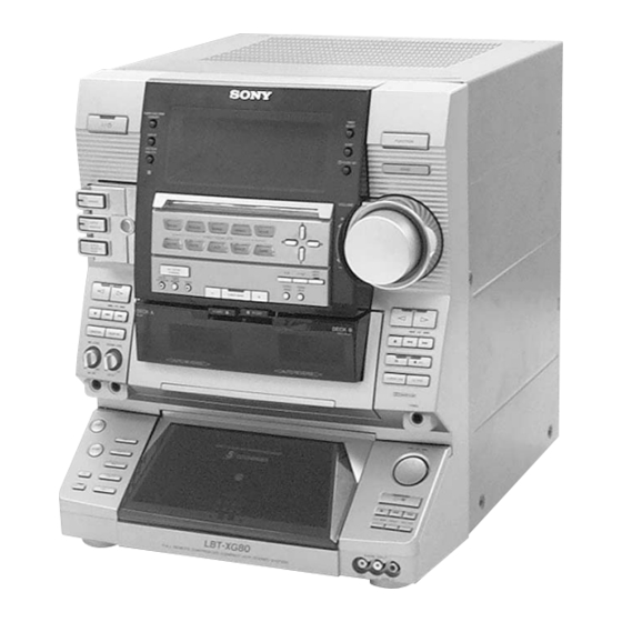
HCD-XG80/XG700 is the amplifier, CD
player, tape deck and tuner section in
LBT-XG80/XG700.
Dolby noise reduction manufactured under license
from Dolby Laboratories Licensing Corporation.
"DOLBY" and the double-D symbol ; are trade-
marks of Dolby Laboratories Licensing Corporation.
Amplifier section
AEP, UK models:
DIN power output (rated) 200 + 200 watts
(6 ohms at 1 kHz, DIN)
Continuous RMS power output (reference)
250 + 250 watts
(6 ohms at 1 kHz, 10% THD)
Music power output (reference)
430 + 430 watts
(6 ohms at 1 kHz, 10% THD)
Other models:
The following measured at AC 120/220/240V, 50 Hz
DIN power output (rated) 240 + 240 watts
(4 ohms at 1 kHz, DIN)
Continuous RMS power output (reference)
320 + 320 watts
(4 ohms at 1 kHz, 10% THD)
Inputs
DJ MIX*:
(phono jacks)
sensitivity 250 mV,
impedance 47 kilohms
GUITAR IN:
(phone jack)
sensitivity 75 mV,
impedance 470 kilohms
PHONO IN:
(phono jacks)
sensitivity 3 mV,
impedance 47 kilohms
MIX MIC:
(phone jack)
sensitivity 1 mV,
impedance 10 kilohms
Sony Corporation
9-929-596-11
2001C0500-1
Audio Entertainment Group
C 2001.3
General Engineering Dept.
HCD-XG80/XG700
Photo: HCD-XG80
CD
Section
TAPE
Section
SPECIFICATIONS
VIDEO IN:
(phono jacks)
sensitivity 250 mV,
impedance 47 kilohms
GAME IN:
(phono jacks)
sensitivity 250 mV,
impedance 47 kilohms
MD IN:
(phono jack)
sensitivity 450 mV,
impedance 47 kilohms
Outputs
DJ MIX*:
(phono jacks)
sensitivity 250 mV,
impedance 1 kilohms
PHONES:
(stereo phone jack)
accepts headphones of 8
ohms or more
VIDEO OUT:
(phono jack)
voltage 250 mV
impedance 1 kilohm
MD OUT:
(phono jacks)
voltage 250 mV
impedance 1 kilohm
FRONT SPEAKER:
HCD-XG80:
accepts impedance of 4 to
16 ohms
HCD-XG700:
accepts impedance of 6 to
16 ohms
* AEP, UK and Mexican models only
Model Name Using Similar Mechanism
CD Mechanism Type
Base Unit Name
Optical Pick-up Name
Model Name Using Similar Mechanism
Tape Transport Mechanism Type
CD player section
System
Laser
Wavelength
Frequency response
Signal-to-noise ratio
Dynamic range
CD OPTICAL DIGITAL OUT
(Square optical connector jack, rear panel)
Wavelength:
Output level
Tape player section
Recording system
Frequency response
(DOLBY NR OFF)
COMPACT DISC DECK RECEIVER
AEP Model
UK Model
HCD-XG700
E Model
HCD-XG80
HCD-LX6/LX50/LX70
CDM37M-5BD32L
BU-5BD32L
KSS-213DH
NEW
TCM-230PWR42
Compact disc and digital
audio system
Semiconductor laser
( =780nm), Emission
duration: continuous
780 – 790 nm
2 Hz – 20 kHz ( 0.5 dB)
More than 90 dB
More than 90 dB
660 nm
–18 dBm
4-track 2-channel stereo
40 – 13,000 Hz ( 3 dB),
using Sony TYPE I cassette
40 – 14,000 Hz ( 3 dB),
using Sony TYPE II cassette
– Continued on next page –
Advertisement
Table of Contents

Related Manuals for Sony HCD-XG80


Summary of Contents for Sony HCD-XG80
- Page 1 SERVICE MANUAL AEP Model UK Model Ver 1.0 2001.03 HCD-XG700 E Model HCD-XG80 HCD-XG80/XG700 is the amplifier, CD player, tape deck and tuner section in LBT-XG80/XG700. Photo: HCD-XG80 Dolby noise reduction manufactured under license Model Name Using Similar Mechanism HCD-LX6/LX50/LX70 from Dolby Laboratories Licensing Corporation.
- Page 2 LINE WITH MARK 0 ON THE SCHEMATIC DIAGRAMS AND IN THE PARTS LIST ARE CRITICAL TO SAFE OPERATION. REPLACE THESE COMPONENTS WITH SONY PARTS WHOSE PART NUMBERS APPEAR AS SHOWN IN THIS MANUAL OR IN SUPPLEMENTS PUB- LISHED BY SONY.
-
Page 3: Table Of Contents
HCD-XG80/XG700 TABLE OF CONTENTS SERVICING NOTES EXPLODED VIEWS ..........4 8-1. Case, Back Panel Section ..........55 GENERAL 8-2. Front Panel Section-1 ............56 8-3. Front Panel Section-2 ............57 Location of Controls ............5 8-4. Chassis Section ............... 58 Setting the Time .............. -
Page 4: Servicing Notes
HCD-XG80/XG700 SECTION 1 SERVICING NOTES • MODEL IDENTIFICATION NOTES ON HANDLING THE OPTICAL PICK-UP – Rear Panel – BLOCK OR BASE UNIT The laser diode in the optical pick-up block may suffer electro- PART No. static break-down because of the potential difference generated by the charged electrostatic load, etc. -
Page 5: General
HCD-XG80/XG700 SECTION 2 This section is extracted from instruction manual. GENERAL LOCATION OF CONTROLS – Front Panel – 2 3 4 5 6 789 w;ql A EJECT Z/Z B EJECT wg (15) FLAT qd (18) SPECTRUM ANALYZER 4 (20) AUDIO L w; (23) FUNCTIONq;... -
Page 6: Setting The Time
HCD-XG80/XG700 – Rear Panel – 1 ANTENNA terminal 2 DJ MIX RETURN/SEND jack (AEP, UK, Mexican models) 3 PHONO IN jack 4 MD IN/OUT jack 5 VIDEO/AUDIO IN jack 6 VIDEO OUT jack 7 FRONT SPEAKER terminal 8 CD DIGITAL OUT OPTICAL terminal... -
Page 7: Disassembly
HCD-XG80/XG700 SECTION 3 DISASSEMBLY • This set can be disassembled in the order shown below. 3-1. DISASSEMBLY FLOW 3-2. CASE (Page 7) 3-3. FRONT PANEL SECTION (Page 8) 3-4. COVER (TC), 3-5. MAIN BOARD, TAPE MECHANISM DECK FAN, D.C. (M901) -
Page 8: Front Panel Section
HCD-XG80/XG700 3-3. FRONT PANEL SECTION 1 wire (flat type) (15 core) (CN303) 1 wire (flat type) 2 two connectors (17 core) (CN304) (CN452, 702) 1 wire (flat type) 3 two screws (13 core) (CN431) (BVTP3 3 screw (BVTP3 4 two lugs... -
Page 9: Main Board, Fan, D.c. (M901)
HCD-XG80/XG700 3-5. MAIN BOARD, FAN, D.C. (M901) 1 wire (flat type) (13 core) (CN441) AEP, UK, Mexican models 3 eight screws (BVTP3 2 jumper plug 8 back panel 3 screw (BVTP3 3 three screws (BVTP3 7 fan, D.C. 9 wire (flat type) (19 core) -
Page 10: Cd Mechanism Deck (Cdm37M-5Bd32L)
HCD-XG80/XG700 3-6. CD MECHANISM DECK (CDM37M-5BD32L) 1 wire (flat type) (19 core) (CN411) 4 three screws (BVTP3 3 four screws (BVTP3 7 Open the cable clamp. 2 connector (CN412) 4 two screws (BVTP3 8 five screws (BVTP3 9 CD mechanism deck... -
Page 11: Base Unit (Bu-5Bd32L)
HCD-XG80/XG700 3-7. BASE UNIT (BU-5BD32L) 3 base unit (BU-5BD32L) 2 boss 1 BU fitting screw 3-8. DISC TABLE Note: When the disc table is installed, adjust the positions of roller cam and mark B as shown in the figure, then set to the groove of disc table. -
Page 12: Test Mode
HCD-XG80/XG700 SECTION 4 TEST MODE [MC Cold Reset] [CD Delivery Mode] • The cold reset clears all data including preset data stored in the • This mode moves the optical pick-up to the position durable to RAM to initial conditions. Execute this mode when returning vibration. - Page 13 HCD-XG80/XG700 [Aging Mode] 2. Tape Deck Section This mode can be used for operation check of tape deck section. • The sequence during the aging mode is following as below. Tape deck section work in parallel. • If an error occurred, stop display that step.
-
Page 14: Mechanical Adjustments
HCD-XG80/XG700 SECTION 5 SECTION 6 MECHANICAL ADJUSTMENTS ELECTRICAL ADJUSTMENTS Precaution DECK SECTION 0 dB = 0.775 V 1. Clean the following parts with a denatured alcohol-moistened swab: Precaution record/playback heads pinch rollers 1. Demagnetize the record/playback head with a head demagne-... - Page 15 HCD-XG80/XG700 Record/Playback Head Azimuth Adjustment Adjustment Location: Playback Head (Deck A). Record/Playback/Erase Head (Deck B). DECK A DECK B Note: Perform this adjustments for both decks Procedure: 1. Mode: Playback (FWD) test tape MAIN board P-4-A100 MD OUT jack (J701) (10 kHz, –...
- Page 16 HCD-XG80/XG700 Specification values: DECK B REC Bias Adjustment J101 PB level: 47.2 to 53.0 mV (– 24.3 to – 23.3 dB) Procedure: 1. Mode: Record Adjustment Location: MAIN board FUNCTION: VIDEO MAIN board – MAIN BOARD (Conductor Side) – VIDEO AUDIO IN jack (J701)
-
Page 17: Cd Section
HCD-XG80/XG700 E-F Balance (1 Track Jump) Check CD SECTION oscilloscope Note: (DC range) 1. CD Block is basically designed to operate without adjustment. There- fore, check each item in order given. BD board 2. Use YEDS-18 disc (3-702-101-01) unless otherwise indicated. - Page 18 HCD-XG80/XG700 MEMO...
-
Page 19: Diagrams
HCD-XG80/XG700 SECTION 7 DIAGRAMS 7-1. BLOCK DIAGRAM – CD SERVO Section – (XG80 : Mexican/XG700) FILTER DIGITAL SIGNAL PROCESSOR, J705 DIGITAL FILTER, D/A CONVERTER IC101 (1/2) RF AMP, 56 53 SEND FOCUS/TRACKING ERROR AMP R-CH IC103 DETECTOR CD D+5V DJ MIX... -
Page 20: Block Diagram - Tuner/Tape Deck Section
HCD-XG80/XG700 7-2. BLOCK DIAGRAM – TUNER/TAPE DECK Section – DECK PROCESS, DECK A/B SELECT, PB/REC EQ AMP, • R-ch is omitted due to same as L-ch. DOLBY NR AMP, ALC, AMS IC301 • SIGNAL PATH RV311 : TUNER (FM/AM) PB LEVEL (L) -
Page 21: Block Diagram - Main Section
HCD-XG80/XG700 7-3. BLOCK DIAGRAM – MAIN Section – DISTORTION DISTORTION (Page 22) ON/OFF SWITCH GUITAR AMP REC-L Q880 – 883 IC853 (Page 20) J802 SPEANA GUITAR AMP MIC AMP (Page 22) GUITAR IC852 IC850 (2/2) RV601 GUITAR LEVEL MD OUT... -
Page 22: Block Diagram - Display/Key Control/Power Supply Section
HCD-XG80/XG700 7-4. BLOCK DIAGRAM – DISPLAY/KEY CONTROL/POWER SUPPLY Section – (Page 21) (Page 21) (Page 21) FLUORESCENT INDICATOR TUBE DRIVER, SUB POWER KEY CONTROL BAND-PASS FILTER TRANSFORMER IC601 IC602 T901 EVER +5V RECT SYSTEM CONTROLLER (IC501) , REGULATOR BPF 0 D902 –... -
Page 23: Note For Printed Wiring Boards And Schematic Diagrams
HCD-XG80/XG700 7-5. NOTE FOR PRINTED WIRING BOARDS AND SCHEMATIC DIAGRAMS • Circuit Boards Location Note on Printed Wiring Board: Note on Schematic Diagram: • X : parts extracted from the component side. TRANS board SUB TRANS board • All capacitors are in F unless otherwise noted. pF: •... -
Page 24: Printed Wiring Board - Bd Board
HCD-XG80/XG700 7-6. PRINTED WIRING BOARD – BD Board – • See page 23 for Circuit Boards Location. TP(GND) TP(VC) TP(RF) (AGCCON) TP(FE) TP(TE) MAIN BOARD TP(FE1) CN411 (Page 34) KSS-213DH • Semiconductor • Semiconductor Location Location Ref. No. Location Ref. No. -
Page 25: Schematic Diagram - Bd Board
HCD-XG80/XG700 7-7. SCHEMATIC DIAGRAM – BD Board – • • See page 35 for Waveforms. See page 47 for IC Block Diagrams. OPTICAL PICK-UP BLOCK (KSS-213DH) D+5V (SW) L-CH R-CH A+5V (SW) CD-DATA CD-CLK MAIN BOARD CN411 SQ-DATA (Page 32) -
Page 26: Printed Wiring Boards - Cd Motor Section
HCD-XG80/XG700 7-8. PRINTED WIRING BOARDS – CD MOTOR Section – • See page 23 for Circuit Boards Location. MAIN BOARD CN412 (Page 34) -
Page 27: Schematic Diagram - Cd Motor Section
HCD-XG80/XG700 7-9. SCHEMATIC DIAGRAM – CD MOTOR Section – • See page 47 for IC Block Diagram. TABLE MOTOR DRIVER LED DRIVE (Page 32) MAIN BOARD CN412 DISC TABLE SENSOR • Voltages and waveforms are dc with respect to ground under no-signal conditions. -
Page 28: Printed Wiring Board - Audio Board
HCD-XG80/XG700 7-10. PRINTED WIRING BOARD – AUDIO Board – • See page 23 for Circuit Boards Location. MAIN BOARD (Page 34) CN303 AUDIO BOARD (24) 1-675-753- (CHASSIS) – B DECK – HPRE101 – A DECK – RECORD/PLAYBACK HP101 ERASE (PLAYBACK) -
Page 29: Schematic Diagram - Audio Board
HCD-XG80/XG700 7-11. SCHEMATIC DIAGRAM – AUDIO Board – • See page 47 for IC Block Diagram. (PALYBACK) PB EQ AMP (DECK A) PB LEVEL (L) (DECK A) R492 1.5K –7 R491 820 PB EQ AMP (DECK B) PB LEVEL (L) (DECK B) R482 1.5K... -
Page 30: Printed Wiring Board - Leaf Sw Board
HCD-XG80/XG700 7-12. PRINTED WIRING BOARD – LEAF SW Board – • See page 23 for Circuit Boards Location. DECK B DECK A PLUNGER PLUNGER (DECK B PLAY) (DECK B 120/70) (DECK A PLAY) (DECK B HALF) (DECK A REC) (DECK A 120/70) -
Page 31: Schematic Diagram - Main Board (1/3)
HCD-XG80/XG700 7-14. SCHEMATIC DIAGRAM – MAIN Board (1/3) – • See page 47 for IC Block Diagram. (Page 33) (Page 32) (Page 32) (Page 39) (Page 32) (Page 33) • Voltages and waveforms are dc with respect to ground under no-signal (detuned) conditions. -
Page 32: Schematic Diagram - Main Board (2/3)
HCD-XG80/XG700 7-15. SCHEMATIC DIAGRAM – MAIN Board (2/3) – • See page 35 for Waveforms. (Page 33) (Page 31) (Page 33) (Page 31) (Page 41) (Page 25) (Page 27) (Page 33) (Page 29) (Page 30) (Page 33) (Page 31) • Voltages and waveforms are dc with respect to ground <... -
Page 33: Schematic Diagram - Main Board (3/3)
HCD-XG80/XG700 7-16. SCHEMATIC DIAGRAM – MAIN Board (3/3) – (Page 32) (Page 39) (Page 31) (Page 32) (Page 32) (Page 37) (Page 32) (Page 31) (Page 37) • Voltages and waveforms are dc with respect to ground under no-signal (detuned) conditions. -
Page 34: Printed Wiring Board - Main Board
HCD-XG80/XG700 7-17. PRINTED WIRING BOARD – MAIN Board – • See page 23 for Circuit Boards Location. J705 J701 DJ MIX VIDEO J702 M901 AUDIO IN RETURN SEND PHONO IN MD IN MD OUT (FAN) VIDEO VIDEO IN VIDEO OUT... - Page 35 HCD-XG80/XG700 • Semiconductor • Waveforms Location – BD Board – – MAIN Board – Ref. No. Location 1 IC101 yj (XTAO) 5 IC101 wh (MDP) (CD Play Mode) 1 IC501 0 (XC-IN) D191 D192 D193 D194 D501 D534 3.1 Vp-p 2.5 Vp-p...
-
Page 36: Printed Wiring Board - Pa Board
HCD-XG80/XG700 7-18. PRINTED WIRING BOARD – PA Board – • See page 23 for Circuit Boards Location. • Semiconductor Location (Page 34) (Page 34) Ref. No. Location MAIN BOARD MAIN BOARD CN902 CN901 D401 D402 D405 PA BOARD D406 (XG700) -
Page 37: Schematic Diagram - Pa Board
HCD-XG80/XG700 7-19. SCHEMATIC DIAGRAM – PA Board – (Page 39) (Page 46) (Page 46) (Page 46) (Page 33) (Page 33) The components identified by mark 0 or dotted • Voltages and waveforms are dc with respect to ground line with mark 0 are critical for safety. -
Page 38: Printed Wiring Boards - Mic/Front Input/Headphones Boards
HCD-XG80/XG700 7-20. PRINTED WIRING BOARDS – MIC/FRONT INPUT/HEADPHONES Boards – • See page 23 for Circuit Boards Location. MIC BOARD (Page 44) • Semiconductor TC-A BOARD Location NO805 Ref. No. Location (Page 34) MAIN BOARD IC850 CN452 IC852 IC853 Q880... -
Page 39: Schematic Diagram - Mic/Front Input/Headphones Boards
HCD-XG80/XG700 7-21. SCHEMATIC DIAGRAM – MIC/FRONT INPUT/HEADPHONES Boards – (Page 45) (Page 33) (Page 31) (Page 37) • Voltages and waveforms are dc with respect to ground under no-signal (detuned) conditions. no mark : TUNER (FM/AM) -
Page 40: Printed Wiring Board - Panel Fl Board
HCD-XG80/XG700 7-22. PRINTED WIRING BOARD – PANEL FL Board – • See page 23 for Circuit Boards Location. PANEL FL BOARD FL601 FLUORESCENT INDICATOR TUBE D601, S608 TIMER POWER SAVE/DEMO SELECT (STANDBY) FUNCTION SLEEP DISPLAY c/CLOCK SET SPECTRUM GAME ANALYZER... -
Page 41: Schematic Diagram - Panel Fl Board
HCD-XG80/XG700 7-23. SCHEMATIC DIAGRAM – PANEL FL Board – • • See page 35 for Waveform. See page 47 for IC Block Diagram. (Page 45) (Page 45) (Page 32) • Voltages and waveforms are dc with respect to ground (Page 43) under no-signal (detuned) conditions. -
Page 42: Printed Wiring Boards - Panel Vr/Illumination Boards
HCD-XG80/XG700 7-24. PRINTED WIRING BOARDS – PANEL VR/ILLUMINATION Boards – • See page 23 for Circuit Boards Location. (Page 40) ILLUMINATION BOARD PANEL FL BOARD CN602 D791 (ILLUMINATION) (11) PANEL VR BOARD (CHASSIS) D717, S713 GROOVE S736 ROTARY ENCODER D708, S719... -
Page 43: Schematic Diagram - Panel Vr/Illumination Boards
HCD-XG80/XG700 7-25. SCHEMATIC DIAGRAM – PANEL VR/ILLUMINATION Boards – • See page 47 for IC Block Diagram. (Page 41) • Voltages and waveforms are dc with respect to ground under no-signal (detuned) conditions. no mark : TUNER (FM/AM) -
Page 44: Printed Wiring Boards - Tc-A/Tc-B/Cd-L/Cd-R (1)/Cd-R (2) Boards
HCD-XG80/XG700 7-26. PRINTED WIRING BOARDS – TC-A/TC-B/CD-L/CD-R (1)/CD-R (2) Boards – • See page 23 for Circuit Boards Location. (Page 40) (Page 40) PANEL FL PANEL FL BOARD BOARD NO601 NO602 CD-L BOARD TC-A BOARD TC-B BOARD LID (CD) OPEN/CLOSE... -
Page 45: Schematic Diagram - Tc-A/Tc-B/Cd-L/Cd-R (1)/Cd-R (2) Boards
HCD-XG80/XG700 7-27. SCHEMATIC DIAGRAM – TC-A/TC-B/CD-L/CD-R (1)/CD-R (2) Boards – (Page 41) (Page 39) (Page 41) -
Page 46: Printed Wiring Boards - Transformer Section
HCD-XG80/XG700 7-28. PRINTED WIRING BOARDS – TRANSFORMER Section– 7-29. SCHEMATIC DIAGRAM – TRANSFORMER Section – • See page 23 for Circuit Boards Location. PA BOARD NO702 (Page 36) (Page 37) TRANS BOARD (Page 37) PA BOARD CN801 (Page 36) (MX) - Page 47 HCD-XG80/XG700 • IC Block Diagrams – BD Board – IC101 CXD2587Q ERROR DIGITAL CORRECTOR ASYMMETRY DIGITAL CORRECTOR OPERATIONAL LRCK AMPLIFIER ANALOG SWITCH PCMD INTERFACE DEMODULATOR CONVERTER EMPH XVDD XTAI TIMING CLOCK LOGIC XTAO XTSL GENERATOR XVSS TES1 AVDD1 TEST AOUT1...
- Page 48 HCD-XG80/XG700 IC103 CXA2568M-T6 HOLD APC PD AMP LC/PD APC LD AMP – LD ON – – – HOLD SW AGC CONT AGC VTH 50 A – RF BOT – – – – RFTC RF SUMMING AMP RF EQ AMP RF I RF O –...
-
Page 49: Main Board
HCD-XG80/XG700 – CD MOTOR Board – IC201 TA8409S VREF BLOCK STANDBY BLOCK HEAT CUT OFF BLOCK OUT2 OUT1 VREF – AUDIO Board – – MAIN Board – IC602 PC1330HA IC191 BA7615N MUTE INVERTER LOGIC COMPARATER SW P1 CONT GND SW R1 GND... -
Page 50: Ic Pin Function Description
HCD-XG80/XG700 7-30. IC PIN FUNCTION DESCRIPTION MAIN BOARD IC501 M30622MAA-A92FP (SYSTEM CONTROLLER (CD MECHANISM CONTROL)) Pin No. Pin Name Description STK-POWER Power amplifier on/off selection signal output “L”: standby mode, “H”: power amplifier on Power on/off control signal output for the audio system (+5V) and deck, panel, audio system POWER (+7V) and FM/AM tuner unit (+10V) “L”: standby mode, “H”: power on... - Page 51 HCD-XG80/XG700 Pin No. Pin Name Description CLOCK-OUT Not used (open) 40, 41 NO-USE Not used (open) Filament on/off selection signal output for the fluorescent indicator tube (FL601) FL OFF “L”: filament off, “H”: filament on Not used in this set STBY RELAY Main power on/off control signal output “L”: standby mode, “H”: power on...
- Page 52 HCD-XG80/XG700 Pin No. Pin Name Description Line muting on/off selection signal output to the HA12215F (IC301) TC-MUTE “L”: muting off, “H”: muting on Recording/playback/pass selection signal output to the HA12215F (IC301) R/PB/PAS “L”: recording mode, “H”: pass, “Hi-z”: playback mode...
- Page 53 HCD-XG80/XG700 PANEL FL BOARD IC601 TMP88CP76F-1B71 (FLUORESCENT INDICATOR TUBE DRIVER, KEY CONTROL) Pin No. Pin Name Description SIRCS Remote control signal input from the remote control receiver (IC702) KEY POWER Power save/demonstration switch (S609 POWER SAVE/DEMO (STANDBY)) input terminal SAVE/DEMO “L”...
- Page 54 HCD-XG80/XG700 Pin No. Pin Name Description 44 to 66 SEG-1 to SEG-23 Segment drive signal output to the fluorescent indicator tube (FL601) LED STANDBY LED drive signal output of the I/1 indicator (D601) “H”: LED on — Power supply terminal (–35V) (for fluorescent indicator tube drive) —...
-
Page 55: Exploded Views
HCD-XG80/XG700 SECTION 8 EXPLODED VIEWS NOTE: • -XX and -X mean standardized parts, so they • Items marked “*” are not stocked since they The components identified by mark 0 or dotted line with mark 0 are may have some difference from the original are seldom required for routine service. -
Page 56: Front Panel Section-1
HCD-XG80/XG700 8-2. FRONT PANEL SECTION-1 TCM-230PWR42 not supplied not supplied supplied supplied supplied not supplied not supplied not supplied Front panel section-2 Ref. No. Part No. Description Remark Ref. No. Part No. Description Remark 4-232-080-01 COVER (TC) 4-959-229-11 DETENT, CASSETTE... -
Page 57: Front Panel Section-2
HCD-XG80/XG700 8-3. FRONT PANEL SECTION-2 not supplied not supplied (PANEL VR board) not supplied (ILLUMINATION board) not supplied supplied with S736 supplied not supplied Ref. No. Part No. Description Remark Ref. No. Part No. Description Remark 4-951-620-01 SCREW (2.6X8), +BVTP... -
Page 58: Chassis Section
HCD-XG80/XG700 8-4. CHASSIS SECTION not supplied not supplied T951 not supplied not supplied not supplied not supplied CDM37M-5BD32L supplied The components identified by mark 0 or dotted line with mark 0 are critical for safety. Replace only with part number not supplied specified. -
Page 59: Tape Mechanism Deck Section-1
HCD-XG80/XG700 8-5. TAPE MECHANISM DECK SECTION-1 (TCM-230PWR42) Tape mechanism deck section-2 HP101 HRPE101 Ref. No. Part No. Description Remark Ref. No. Part No. Description Remark 3-376-464-11 SCREW (+PTT 2.6X6), GROUND POINT 3-017-366-01 BASE (PINCH LEVER REV) 3-911-116-42 RIVET, PUSH 3-016-567-02 SPRING (CASSETTE), LEAF... -
Page 60: Tape Mechanism Deck Section-2 (Tcm-230Pwr42)
HCD-XG80/XG700 8-6. TAPE MECHANISM DECK SECTION-2 (TCM-230PWR42) Ref. No. Part No. Description Remark Ref. No. Part No. Description Remark X-4952-881-1 CHASSIS ASSY, MAIN 4-228-450-01 SPRING (REVERSE SLIDER), TORSION 3-041-946-01 BELT (CAPSTAN B) 3-019-208-01 WASHER, STOPPER 4-227-239-01 BELT (CAPSTAN C) A-2004-795-A CHASSIS (A) ASSY, SUB... -
Page 61: Cd Mechanism Deck Section (Cdm37M-5Bd32L)
HCD-XG80/XG700 8-7. CD MECHANISM DECK SECTION (CDM37M-5BD32L) supplied M201 supplied Ref. No. Part No. Description Remark Ref. No. Part No. Description Remark 4-987-976-01 SCREW, STEP * 514 A-4673-765-A CD MOTOR BOARD, COMPLETE 4-944-490-01 BELT (TIMING) 4-978-426-01 INDICATOR (NO.) A-4660-978-A GEAR (PULLEY) ASSY... -
Page 62: Base Unit Section (Bu-5Bd32L)
HCD-XG80/XG700 8-8. BASE UNIT SECTION (BU-5BD32L) M101 M102 The components identified by mark 0 or dotted line with mark 0 are critical for safety. Replace only with part number specified. Ref. No. Part No. Description Remark Ref. No. Part No. -
Page 63: Electrical Parts List
HCD-XG80/XG700 SECTION 9 ELECTRICAL PARTS LIST AUDIO NOTE: • Due to standardization, replacements in the • Items marked “*” are not stocked since they The components identified by mark 0 or dotted line with mark parts list may be different from the parts speci- are seldom required for routine service. - Page 64 HCD-XG80/XG700 AUDIO Ref. No. Part No. Description Remark Ref. No. Part No. Description Remark R609 1-249-433-11 CARBON 1/4W C157 1-163-009-11 CERAMIC CHIP 0.001uF R611 1-249-409-11 CARBON 1/4W C159 1-163-019-00 CERAMIC CHIP 0.0068uF 10% R612 1-249-409-11 CARBON 1/4W C161 1-126-206-11 ELECT CHIP 100uF 6.3V...
- Page 65 HCD-XG80/XG700 CD MOTOR CD-L CD-R (1) Ref. No. Part No. Description Remark Ref. No. Part No. Description Remark R162 1-216-101-00 METAL CHIP 150K 1/10W < LED > R171 1-216-078-00 RES-CHIP 1/10W R172 1-216-073-00 METAL CHIP 1/10W D741 8-719-058-04 LED SEL5223S-TP15 (NON-STOP)
- Page 66 HCD-XG80/XG700 CD-R (2) FRONT INPUT HEADPHONES ILLUMINATION LEAF SW Ref. No. Part No. Description Remark Ref. No. Part No. Description Remark ILLUMINATION BOARD 1-680-183-11 CD-R (2) BOARD ******************* ************** < CAPACITOR > < CAPACITOR > C791 1-162-974-11 CERAMIC CHIP 0.01uF...
- Page 67 HCD-XG80/XG700 LEAF SW MAIN Ref. No. Part No. Description Remark Ref. No. Part No. Description Remark S1006 1-771-333-11 SWITCH, LEAF (DECK B HALF) C171 1-126-964-11 ELECT 10uF S1008 1-771-205-11 SWITCH, LEAF (DECK B 120/70) C172 1-164-363-11 CERAMIC CHIP 560PF S1009...
- Page 68 HCD-XG80/XG700 MAIN Ref. No. Part No. Description Remark Ref. No. Part No. Description Remark C601 1-162-959-11 CERAMIC CHIP 330PF C602 1-162-927-11 CERAMIC CHIP 100PF C914 1-126-916-11 ELECT 1000uF 6.3V C603 1-162-927-11 CERAMIC CHIP 100PF C932 1-126-964-11 ELECT 10uF C604 1-126-961-11 ELECT 2.2uF...
- Page 69 HCD-XG80/XG700 MAIN Ref. No. Part No. Description Remark Ref. No. Part No. Description Remark FL503 1-233-289-21 FILTER, EMI (SMD) Q332 8-729-029-86 TRANSISTOR DTC124ESA < IC > Q333 8-729-140-04 TRANSISTOR 2SB1116A-L Q334 8-729-029-86 TRANSISTOR DTC124ESA IC101 8-759-571-54 IC M62493FP Q335 8-729-029-86 TRANSISTOR...
- Page 70 HCD-XG80/XG700 MAIN Ref. No. Part No. Description Remark Ref. No. Part No. Description Remark R163 1-216-847-11 METAL CHIP 150K 1/16W R358 1-216-829-11 METAL CHIP 4.7K 1/16W (XG700) R163 1-216-848-11 METAL CHIP 180K 1/16W R359 1-216-839-11 METAL CHIP 1/16W (XG80) R371...
- Page 71 HCD-XG80/XG700 MAIN Ref. No. Part No. Description Remark Ref. No. Part No. Description Remark R653 1-216-841-11 METAL CHIP 1/16W R559 1-216-809-11 METAL CHIP 1/16W R654 1-216-820-11 METAL CHIP 1/16W R561 1-216-809-11 METAL CHIP 1/16W (XG700) R563 1-216-809-11 METAL CHIP 1/16W...
- Page 72 HCD-XG80/XG700 MAIN Ref. No. Part No. Description Remark Ref. No. Part No. Description Remark RV351 1-238-600-11 RES, ADJ, CARBON 10K R807 1-249-429-11 CARBON 1/4W R809 1-249-417-11 CARBON 1/4W < VIBRATOR > R850 1-249-417-11 CARBON 1/4W R852 1-249-441-11 CARBON 100K 1/4W X501 1-567-098-41 VIBRATOR, CRYSTAL (32.768kHz)
- Page 73 HCD-XG80/XG700 Ref. No. Part No. Description Remark Ref. No. Part No. Description Remark C811 1-130-491-00 MYLAR 0.047uF D406 8-719-991-33 DIODE 1SS133T-77 D801 8-719-991-33 DIODE 1SS133T-77 C812 1-130-491-00 MYLAR 0.047uF C813 1-162-306-11 CERAMIC 0.01uF D802 8-719-110-49 DIODE RD18ESB2 C814 1-162-294-31 CERAMIC 0.001uF...
- Page 74 HCD-XG80/XG700 Ref. No. Part No. Description Remark Ref. No. Part No. Description Remark R828 1-247-903-00 CARBON 1/4W < RESISTOR > R831 1-249-441-11 CARBON 100K 1/4W R832 1-249-441-11 CARBON 100K 1/4W 0 R401 1-215-867-00 METAL OXIDE (XG80) R833 1-247-856-00 CARBON 1/4W...
- Page 75 HCD-XG80/XG700 PANEL FL Ref. No. Part No. Description Remark Ref. No. Part No. Description Remark A-4475-589-A PANEL FL BOARD, COMPLETE < RESISTOR > ************************ R601 1-249-429-11 CARBON 1/4W 4-225-511-01 HOLDER FL TUBE R602 1-249-437-11 CARBON 1/4W 4-949-935-81 CUSHION (FL) R603...
- Page 76 HCD-XG80/XG700 PANEL FL PANEL VR Ref. No. Part No. Description Remark Ref. No. Part No. Description Remark R661 1-249-410-11 CARBON 1/4W IC702 8-759-827-68 IC NJL62H400A-1 (REMOTE CONTROL RECEIVER) < SWITCH > < COIL > S601 1-762-875-21 SWITCH, KEYBOARD (DISPLAY) S602...
- Page 77 HCD-XG80/XG700 PANEL VR SUB TRANS TABLE SENSOR TC-A Ref. No. Part No. Description Remark Ref. No. Part No. Description Remark < RELAY > R786 1-249-407-11 CARBON 1/4W R787 1-249-407-11 CARBON 1/4W 0 RY901 1-755-276-11 RELAY, POWER R788 1-249-407-11 CARBON 1/4W...
- Page 78 HCD-XG80/XG700 TC-B TRANS Ref. No. Part No. Description Remark Ref. No. Part No. Description Remark 1-680-172-11 TC-B BOARD 0 F962 1-533-949-31 FUSE, CYLINDRICAL (TIME LUG) (T8AL/250V) 0 F963 1-532-506-31 FUSE (T6.3AL/250V) *********** 0 F964 1-532-506-31 FUSE (T6.3AL/250V) < LED >...
- Page 79 HCD-XG80/XG700 Ref. No. Part No. Description Remark Ref. No. Part No. Description Remark ACCESSORIES & PACKING MATERIALS ******************************* 1-569-008-21 ADAPTOR, CONVERSION (EA, SP) 1-770-019-11 ADAPTOR, CONVERSION PLUG 3P (UK) The components identified by mark 0 or dotted line with mark 0 are critical for safety.
- Page 80 HCD-XG80/XG700 REVISION HISTORY Clicking the version allows you to jump to the revised page. Also, clicking the version at the upper right on the revised page allows you to jump to the next revised page. Ver. Date Description of Revision...