Advertisement
Table of Contents
- 1 Specifications
- 2 Panel Layout
- 3 Block Diagram
- 4 Circuit Board Layout
- 5 Wiring
- 6 Disassembly Procedure
- 7 Lsi Pin Description
- 8 IC Block Diagram
- 9 Circuit Boards
- 10 Test Program
- 11 Error Messages
- 12 MIDI Implementation Chart
- 13 Parts List
- 14 Guitar Pre-Amplifier with Effects
- 15 Overall Assembly
- 16 Electrical Parts
- Download this manual
See also:
Owner's Manual
GUITAR PRE-AMPLIFIER WITH EFFECTS
This document is printed on chlorine free (ECF) paper with soy ink.
GA
011537
20001001-39800
SERVICE MANUAL
CONTENTS
SPECIFICATIONS
PANEL LAYOUT
BLOCK DIAGRAM
CIRCUIT BOARD LAYOUT
WIRING
................................................................... 11
DISASSEMBLY PROCEDURE
LSI PIN DESCRIPTION
IC BLOCK DIAGRAM
CIRCUIT BOARDS
TEST PROGRAM
ERROR MESSAGES
MIDI IMPLEMENTATION CHART ......................................... 32
PARTS LIST
OVERALL CIRCUIT DIAGRAM
................................................ 3/4
.................................... 5
............................ 8
............... 10
............................ 12
.............................. 15
................................... 18
........................................ 20
................................. 28
............................. 31
HAMAMATSU, JAPAN
1.57K-786 I.T
Printed in Japan 2000.09
DG-Stomp
1
Advertisement
Table of Contents

Related Manuals for Yamaha DG-Stomp


Summary of Contents for Yamaha DG-Stomp
- Page 1 DG-Stomp GUITAR PRE-AMPLIFIER WITH EFFECTS SERVICE MANUAL CONTENTS SPECIFICATIONS ..........3/4 PANEL LAYOUT ........5 BLOCK DIAGRAM ......8 CIRCUIT BOARD LAYOUT ....10 WIRING ..............11 DISASSEMBLY PROCEDURE ......12 LSI PIN DESCRIPTION ......15 IC BLOCK DIAGRAM ........18 CIRCUIT BOARDS ........
- Page 2 IMPOR TANT NOTICE This manual has been provided for the use of authorized Yamaha Retailers and their service personnel. It has been assumed that basic service procedures inherent to the industry, and more specifically Yamaha Products, are already known and under- stood by the users, and have therefore not been restated.
-
Page 3: Specifications
DG-Stomp SPECIFICATIONS Digital Section Connections/Jacks • Full Digital Signal Processing INPUT: Standard Monaural Phone Jack • 8 Channel Preamp OUTPUT L/MONO, R: Standard Monaural Phone Jack • Digital Effects PHONES: Standard Stereo Phone Jack • Compressor EXP. PEDAL: Standard Stereo Phone Jack •... - Page 4 DG-Stomp...
-
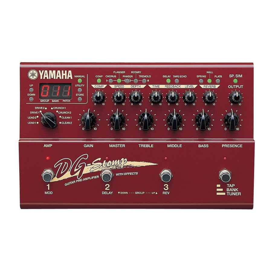
Page 5: Panel Layout
DG-Stomp PANEL LAYOUT Top Panel Display & Main Section Amp Section Effect Section Foot Switch Section Display & Main Section Up Button (UP) Down Button (DOWN) Manual Button (MANUAL) Utility Button (UTILITY) Store Button (STORE) Display... - Page 6 DG-Stomp Amp Section Amp Select Switch (LEAD1-CLEAN2) Gain Control (GAIN) Master Volume (MASTER) Tone Controls Output Level Control (OUTPUT) Speaker Simulator Button (SP. SIM) Effect Section Compressor Button (COMP) Compressor Knob (COMP) Modulation Group Effect Buttons (CHORUS/FLANGER/PHASER/ROTARY/TREMOLO) Speed Knob (SPEED)
- Page 7 DG-Stomp Foot Switch Section Foot Switches 1, 2, 3 Bank Switch (TAP/BANK/TUNER) Rear Panel Power Switch (STAND-BY ON/OFF) Power Adaptor Jack (AC IN 12V 700mA) MIDI OUT Jack MIDI IN Jack Digital Out Jack (DIGITAL OUT) EXP Pedal Jack (EXP. PEDAL)
-
Page 8: Block Diagram
DG-Stomp BLOCK DIAGRAM CN301 IC101 IC102 IC102 CN301 IC103 IC104 IC103 IC2 , IC3 IC10 , IC11 AN0~AN3 , SELECT-A , SELECT-B PB0~PB7 , SW-R0~R3 ( DM-CN3 ) ( DM-CN1 ) ( PN-CN304 ) ( PN-CN302 ) IC308 IC309... - Page 9 DG-Stomp IC105 IC105 IC106 IC106 15 , 17 LED-FOOT TXDO , RXDO LED-REV LED-MOD CLD , CIN , CCK SW-001 , SW-010 , SW-100 , SW-LINE 18 , 19 , ( DM-CN2 ) ( PN-CN303 ) IC112 IC113 IC114 KEC-54203...
-
Page 10: Circuit Board Layout
DG-Stomp CIRCUIT BOARD LAYOUT... -
Page 11: Wiring
DG-Stomp WIRING CN301 CN302 CN305 CN304 CN303 V610850 CN306 V611470 V611450 V611460 Note) When installing the DM circuit board, use care not to have the wire assembly caught by the bottom case. CN103 V611480... -
Page 12: Disassembly Procedure
DG-Stomp DISASSEMBLY PROCEDURE Bottom Case Remove the six (6) screws marked [30]. The bottom case can then be removed. (Fig. 1) [30] Bottom [30] [30]: Bind Head Tapping Screw-B 3.0x8 MFZN2BL (EP600190) Fig.1 DM Circuit Board 2-1. Remove the bottom case. (See Procedure 1.) 2-2. - Page 13 DG-Stomp Topcover Battery VN103500 VN103600(Battery holder for VN103500) • Notice for back-up battery removal Push the battery as shows in figure, then the battery will pop up. [10c-b] [10c]: Bind Head Tapping Screw-B 3.0x8 MFZN2BL (EP600190) [10e]: Hexagonal Nut 9.0 12x2 MFNI33 (LX200060) Fig.2...
- Page 14 DG-Stomp Heat Sink 4-1. Remove the two (2) screws marked [A-a] from the soldered face of the DM circuit board and the three (3) screws marked [A-b] from IC112, IC113 and IC114. The heat sink can then be removed from the DM circuit board.
-
Page 15: Lsi Pin Description
DG-Stomp LSI PIN DESCRIPTION HD6413002FP16 (XQ375A00) CPU DM: IC12 NAME FUNCTION NAME FUNCTION Port A Address bus Power supply Address bus Port B Ground P60//WAIT PB6//DREQ0 P61//BREQ Port 6 PB7//DREQ1 /RESO Reset P62//BACK Ground Ø Øout P90/TXD0 Transmit data (MIDI OUT) - Page 16 DG-Stomp YSS910-S (XV988A00) DSP6 (Digital Signal Processor) DM: IC8, IC9 NAME FUNCTION NAME FUNCTION Power supply (3.3 V) Ground Ground DB13 System master clock input (60 MHz or 30 MHz) DB14 System master clock output (High or 30 MHz) DB15...
- Page 17 DG-Stomp YM3437C-F (XM530A00) DIT2 (Digital Format Interface Transmitter) DM: IC17 NAME FUNCTION NAME FUNCTION Ground MUTE Mute MCLK Master clock input Validity flag DIN/BCLK/WCLK format select C,U bit clock input/C bit data input DM1,DM0=0,0 DSP,LDSP (64 bit,LSB first) C,U bit data input/U bit data input...
-
Page 18: Ic Block Diagram
DG-Stomp IC BLOCK DIAGRAM MB3790PF(XR967A00) DM: IC4 ASSP CONTROL N.C. CONTROL 590k Reference 2.65V BAT1 N.C. Voltage ALARM1 1.24V Power Supply Circuit 2.37V ALARM2 SENSE BAT2 SENSE ALARM1 RESET ALARM1 RESET 240k V th:3V RESET RESET V th:1.5V 74AHC32DT XZ103A00... - Page 19 DG-Stomp 74HC374DT(XZ102A00) 74HC4052DT(XZ101A00) NJM072M(XC458A00) PN: IC301~IC307 PN: IC308, IC309 DM: IC101 D-FF Multiplexer OP AMP +DC Voltage Output A OUT PUT Supply CONTROL – + Inverting Output B Input A – Non-Inverting Inverting D CK Input A Input B –DC Voltage Non-Inverting –V...
-
Page 20: Circuit Boards
DG-Stomp CIRCUIT BOARDS DM Circuit Board CN101: N.C. CN103: to PN1/2-CN301 CN102: N.C. to PN Battery VN103500 VN103600(Battery holder for VN103500) • Notice for back-up battery removal Push the battery as shows in figure, then the battery will pop up. - Page 21 DG-Stomp to PN1/2-CN302 to PN1/2-CN303 to PN1/2-CN304 CN104: N.C. Component side DM: CNA-V588000...
- Page 22 DG-Stomp DM Circuit Board...
- Page 23 DG-Stomp Pattern side...
- Page 24 DG-Stomp PN 1/2 Circuit Board to PN2/2-CN306 to DM-CN3 PN 2/2 Circuit Board LD302, LD303, LD304 and LD306 installation Anode PN: CNA-V587990...
- Page 25 DG-Stomp to DM-CN103 to DM-CN2 to DM-CN1 Component side Component side...
- Page 26 DG-Stomp PN 1/2 Circuit Board PN 2/2 Circuit Board to SW to SW...
- Page 27 DG-Stomp Pattern side to PN1/2-CN305 to SW to SW Pattern side...
-
Page 28: Test Program
DG-Stomp TEST PROGRAM A. Connect each terminal as follows • INPUT Monaural input • OUT L/MONO Monaural output (RL47Kohm) • OUT R Monaural output (RL47Kohm) • HEAD PHONES Stereo output (323ohm each) • EXP. PEDAL Connect VR of B50K. Pin 1 of JK: MIN of VR, Pin 2 of JK: MAX of VR, Pin3 of JK: CENTER of VR •... - Page 29 DG-Stomp SW Check • Using the UP and DOWN switches, select “1” and then press the STORE switch. • Starting with the UP switch, press the switches whose LED lights up one after another. After “SP .SIM”, “BANK”, “3”, “2” and “1”, all LED segments should light up and then go out.
- Page 30 DG-Stomp 6: DSP Electric Characteristic • Using the UP and DOWN switches, select “6” and then press the STORE switch.The output level becomes the same when the right end No. is “0” and when it is “1”. • The output level, noise level and distortion rate can be checked by inputting the signal for measurement (by shorting the input with GND for the noise level check).
-
Page 31: Error Messages
DG-Stomp ERROR MESSAGES If an error occurs during operation, one of the following error message numbers will appear on the display. : MIDI Receive Buffer Full CAUSE: Too much MIDI data is being received by the DG amplifier at one time. -
Page 32: Midi Implementation Chart
DG-Stomp YAMAHA [ Guitar Pre Amplifier with Multi Effects] Date:30-Jun-2000 Model DG stomp MIDI Implementation Chart Version : 1.0 +----------------------------------------------------------------------+ Transmitted Recognized Remarks Function ... : :-------------------+----------------+----------------+----------------: :Basic Default : 1 - 16 : 1 - 16, off : memorized... -
Page 33: Parts List
GUITAR PRE-AMPLIFIER WITH EFFECTS PARTS LIST CONTENTS OVERALL ASSEMBLY ..........2 ELECTRICAL PARTS ..........4 Notes : DESTINATION ABBREVIATIONS A : Australian model M : South African model B : British model O : Chinese model C : Canadian model Q : South-east Asia model D : German model T : Taiwan model... -
Page 34: Overall Assembly
DG-Stomp OVERALL ASSEMBLY P10-1 P10-2 10d-2 10d-1... - Page 35 DG-Stomp PART NO. DESCRIPTION REMARKS REF NO. RANK OVERALL ASSEMBLY DG-STOMP Overall Assembly (V573350) Top Cover Assembly (V573420) V 5 7 3 4 3 0 0 Top Cover V 5 7 3 4 5 0 0 Meter Cover EP600190 Bind Head Tapping Screw-B 3.0X8 MFZN2BL...
-
Page 36: Electrical Parts
DG-Stomp ELECTRICAL PARTS PART NO. DESCRIPTION REMARKS REF NO. RANK ELCTRIC PARTS V 5 8 8 0 0 0 0 Circuit Board AAX19500 Circuit Board AAX19510 Circuit Board (Foot SW Sheet) V 5 8 8 0 0 0 0 Circuit Board... - Page 37 DG-Stomp PART NO. DESCRIPTION REMARKS REF NO. RANK C135 V 6 1 9 7 0 0 0 Electrolytic Cap.-BP 47.00 25.0V C136 UX063100 Electrolytic Cap.(chip) 1000P 50V K C137 V 6 1 9 7 1 0 0 Electrolytic Cap.-BP 10.00 35.0V...
- Page 38 DG-Stomp PART NO. DESCRIPTION REMARKS REF NO. RANK IC10 XV839A00 SDM4260CLU-6S IC11 XV077A00 MSM514260C-60JS IC11 XV839A00 SDM4260CLU-6S IC12 XQ375A00 HD6413002FP16 IC13 VN686000 Photo Coupler PC410T IC13 VR903700 Photo Coupler HCPL-M600 IC14 XZ109A00 74HC244DT BUS BUFFER IC15 74HC244DT BUS BUFFER XZ109A00...
- Page 39 DG-Stomp PART NO. DESCRIPTION REMARKS REF NO. RANK R105 RG007220 Carbon Resistor (chip) 22K 0.1 J R106 RG007120 Carbon Resistor (chip) 12K 0.1 J R108 RG107100 Carbon Resistor (chip) 10K 0.1 F R109 RG107220 Carbon Resistor (chip) 22K 0.1 F...
- Page 40 DG-Stomp PART NO. DESCRIPTION REMARKS REF NO. RANK VU682100 Quartz Crystal Unit 30.00M HZ DOC-49S2 VE463500 Quartz Crystal Unit AT-49/12.0000MHZ X101 VN277000 Quartz Crystal Unit 24.576M AF3817CQA ZD101 VU170900 Zener Diode UDZ 2.0BTE-17 2.0V ZD102 VU170900 Zener Diode UDZ 2.0BTE-17 2.0V...
- Page 41 DG-Stomp OVERALL CIRCUIT DIAGRAM 1/2 ( DM ) DG-Stomp PHOTO COUPLER ASSP 256K RAM 256K RAM 8M ROM BUFFER BUFFER BUFFER DSP6 DSP6 4M ROM R27 R28 : installed : not installed INVERTER REGULATOR 3.3V 4M ROM DIT2 OPAMP OPAMP ADC &...
- Page 42 DG-Stomp OVERALL CIRCUIT DIAGRAM 2/2 ( PN 1/2 , PN 2/2 ) DG-Stomp D-FF D-FF D-FF D-FF D-FF D-FF OUTPUT to DM-CN103 to DM-CN1 to DM-CN2 D-FF AMP SELECT GAIN MASTER TREBLE MIDDLE BASS PRESENCE COMP SPEED DEPTH TIME FEEDBACK...