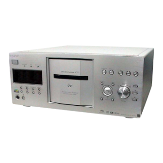
Sony DVP-CX777ES Service Manual
Cd/dvd player
Hide thumbs
Also See for DVP-CX777ES:
- Operating instructions manual (113 pages) ,
- Integration notes (4 pages) ,
- Specifications (2 pages)
Table of Contents
Advertisement
Quick Links
SERVICE MANUAL
Ver 1.1 2004.09
E
S
R
NERGY
TAR
is a U.S. registered mark.
E
S
R
As an
NERGY
TAR
Partner, Sony
Corporation has determined that this product
E
S
R
meets the
NERGY
TAR
guidelines for
energy efficiency.
System
Laser: Semiconductor laser
λ = 780 nm for CD
λ = 650 nm for SA-CD and DVD
Emission duration: continuous
Signal format system: NTSC
Audio characteristics
Frequency response: DVD VIDEO (PCM
96 kHz): 2 Hz to 44 kHz (44 kHz: –2 dB
±1 dB), Super Audio CD: 2 Hz to
100 kHz (50 kHz: –3 dB ±1 dB), CD:
2 Hz to 20 kHz (±0.5 dB)
Signal-to-noise ratio (S/N ratio): 115 dB
(LINE OUT AUDIO L/R 1/2 jacks only)
Harmonic distortion: 0.003 %
Dynamic range: DVD VIDEO/Super Audio
CD: 103 dB, CD: 99 dB
Wow and flutter: Less than detected value
(±0.001% W PEAK)
Sony Corporation
9-961-043-02
2004I05-1
Audio Group
C 2004.09
Published by Sony Engineering Corporation
DVP-CX777ES
Model Name Using Similar Mechanism NEW
CD/DVD Mechanism Type
Base Unit Name
Optical Pick-up Name
SPECIFICATIONS
Outputs
(Jack name: Jack type/Output level/Load
impedance)
LINE OUT AUDIO L/R 1/2: Phono jack/
2 Vrms/10 kilohms
DIGITAL OUT (OPTICAL): Optical
output jack/–18 dBm (wave length:
660 nm)
DIGITAL OUT (COAXIAL): Phono jack/
0.5 Vp-p/75 ohms
5.1CH OUTPUT: Phono jack/2 Vrms/
10 kilohms
COMPONENT VIDEO OUT (Y, P
P
/C
): Phono jack/Y: 1.0 Vp-p/P
R
R
P
/C
: interlace*=0.648 Vp-p,
R
R
progressive or interlace**=0.7 Vp-p/
75 ohms
* BLACK LEVEL is ON
** BLACK LEVEL is OFF
LINE OUT VIDEO 1/2: Phono jack/
1.0 Vp-p/75 ohms
S VIDEO OUPUT 1/2: 4-pin mini DIN/
Y: 1.0 Vp-p/C: 0.286 Vp-p /75 ohms
S-LINK (CONTROL S IN): Mini jack
Canadian Model
General
Power requirements:
120 V AC, 60 Hz
Power consumption: 24 W
Dimensions (approx.): 430 × 189 × 545 mm
(17 × 7
× 21
1
/
2
depth) incl. projecting parts
Mass (approx.): 10 kg (22 lb 1 oz)
Operating temperature: 5 ° C to 35 ° C
°
°
(41
F to 95
F)
Operating humidity: 25 % to 80 %
Supplied accessories
/C
,
B
B
• Audio/video cord (pinplug × 3 y pinplug
/C
,
B
B
× 3) (1)
• Remote commander (remote) (1)
• Size AA (R6) batteries (2)
Specifications and design are subject to
change without notice.
CD/DVD PLAYER
US Model
CDM62-DVBU26
DVBU26
KHM-290AAA
in.) (width/height/
1
/
2
Advertisement
Table of Contents

Related Manuals for Sony DVP-CX777ES


Summary of Contents for Sony DVP-CX777ES
- Page 1 LINE OUT VIDEO 1/2: Phono jack/ 1.0 Vp-p/75 ohms S VIDEO OUPUT 1/2: 4-pin mini DIN/ Y: 1.0 Vp-p/C: 0.286 Vp-p /75 ohms S-LINK (CONTROL S IN): Mini jack CD/DVD PLAYER Sony Corporation 9-961-043-02 2004I05-1 Audio Group C 2004.09 Published by Sony Engineering Corporation...
-
Page 2: Self Diagnosis Function
To prevent a malfunction, the (xx is a number) player has performed the self-diagnosis function. , Contact your nearest Sony dealer or local authorized Sony service facility and give the 5- character service number. Example: E 61 10 Note: Refer to the “4. TEST MODE” (page 23) - Page 3 OPERATION. REPLACE THESE COMPONENTS WITH DE FONCTIONNEMENT. NE REMPLACER CES COM- SONY PARTS WHOSE PART NUMBERS APPEAR AS POSANTS QUE PAR DES PIÈCES SONY DONT LES SHOWN IN THIS MANUAL OR IN SUPPLEMENTS PUB- NUMÉROS SONT DONNÉS DANS CE MANUEL OU LISHED BY SONY.
-
Page 4: This Player Can Play The
DVP-CX777ES • Music discs encoded with copyright protection Example of discs that the player This Player Can Play the technologies This product is designed to playback discs that cannot play Following Discs conform to the Compact Disc (CD) standard. Recently, various music discs encoded with... -
Page 5: Table Of Contents
DVP-CX777ES TABLE OF CONTENTS SELF DIAGNOSIS FUNCTION 7-24. Printed Wiring Board – DRIVER Board – ....74 ........7-25. Schematic Diagram – DRIVER Board – ....... 75 7-26. Printed Wiring Boards SERVICING NOTES ..........6 – MOTOR/SWITCH Section – ........76 7-27. -
Page 6: Servicing Notes
DVP-CX777ES Ver 1.1 SECTION 1 SERVICING NOTES CHECK OF POWER BOARD WITH THE POWER ON NOTES ON HANDLING THE OPTICAL PICK-UP It is possible to analyze the defect with only POWER board power BLOCK OR BASE UNIT The laser diode in the optical pick-up block may suffer electro-... - Page 7 DVP-CX777ES ALIGNMENT OF GEAR (CAM) PHASE WITH DOOR CLEANING OF OPTICAL PICK-UP ASSY door assy gear (cam) optical pick-up pulley assy Remove the pulley assy, and Align a slit of door assy with a marking on clean the lens of optical pick-up the bottom land of gear tooth when the gear through this hole.
- Page 8 DVP-CX777ES When installing the cables, it is made to make it crawl in a chassis. cables driver board cables It is made to contact and for there not to be a power block and cables. AV board AV board cables...
- Page 9 DVP-CX777ES SERVICE POSITION – MB board – Connect the jig (J-2501-086-A) to MB board (CN102) and panel-L board (CN1005). MB board (CN102) panel-L board (CN1005) – Optical pick-up block – optical pick-up (DVBU26)
-
Page 10: General
DVP-CX777ES SECTION 2 This section is extracted from instruction manual. GENERAL Front panel display Front panel When playing back a DVD VIDEO/DVD-RW Current play All discs mode mode Lights up when you can Disc type Playing status change the angle... -
Page 11: Disassembly
DVP-CX777ES SECTION 3 DISASSEMBLY • This set can be disassembled in the order shown below. 3-1. DISASSEMBLY FLOW Note 1: The process described in can be performed in any order. Note 2: Without completing the process described in , the next process can not be performed. -
Page 12: Case (Es) Assy
DVP-CX777ES Note: Follow the disassembly procedure in the numerical order given. 3-2. CASE (ES) ASSY 5 case (ES) assy 3 three flat head screws 4 two flat head screws 1 two flat head screws 2 two flat head screws 3-3. -
Page 13: Av Board
DVP-CX777ES 3-4. AV BOARD 5 +BV sumitite (B3) 9 connector (CN201) 4 screw (BVTP 3 × 8) 6 harness qd AV board 8 two wires (flat type) qs connector (CN204) (23 core: CN202, 27 core: CN203) 2 wire (flat type) -
Page 14: Front Panel Section
DVP-CX777ES 3-6. FRONT PANEL SECTION 2 screw (BVTP 3 × 8) 3 two screws (BVTP 3 × 8) 4 claw 5 claw 6 front panel section 1 five screws (BV/ring) 3-7. COVER (PT)/(CDM) 1 screw 4 six screws (BVTP 3 × 8) -
Page 15: Dvbu26 Assy
DVP-CX777ES 3-8. DVBU26 ASSY 1 three screws (BVTP 3 × 8) 2 screw (BVTP 3 × 8) 5 bracket (top 400) block 3 two screws (BVTP 3 × 8) 6 torsion holder (magnet) block 9 DVBU26 assy q; 8 washer... -
Page 16: Table (400) Assy
DVP-CX777ES 3-10. TABLE (400) ASSY 3 table (400) assy 1 screw (M3 × 14) 2 guide block (door) Note for installation When installing the guide (door), align the positions as shown. 4 10 washer 3-11. DOOR BLOCK, BASE (DOOR) ASSY 2 three screws (BVTP 3 ×... -
Page 17: Dc Motor (Door) (M603)
DVP-CX777ES 3-12. DC MOTOR (DOOR) (M603) 1 belt 5 DC motor (door) (M603) 4 door motor board 3 Remove two solderings. 2 two screws (BVTP 3 × 8) 3-13. HOLDER (TABLE SENSOR 400) 2 connector (CN83) 1 four screws (BVTP 3 × 8) -
Page 18: Sens Out Board, D. Sens In Board
DVP-CX777ES 3-14. D. SENS OUT BOARD, D. SENS IN BOARD 6 screw (PTTWH 3 × 6) 1 screw (PTTWH 3 × 6) 7 D. sens in board 2 two step screws (T1) 4 screw (PSW 3 × 8) 5 D. sens out board 3 bracket (sensor 400) 3-15. -
Page 19: Door Sw Board
DVP-CX777ES 3-16. DOOR SW BOARD 3 screw (PTPWH 2.6 × 8) 1 screw (PTPWH 2.6 × 8) 5 two screws (BVTP 2.6 × 8) 2 gear (cam) 6 door SW board 4 gear (B) Precaution during the gear (cam) installation... -
Page 20: Lock Sw Board, Loading Sw Board
DVP-CX777ES 3-17. LOCK SW BOARD, LOADING SW BOARD 2 screw (BVTP3 × 8) 1 Rotate the pulley (400) in the direction of the arrow A fully. 3 Rotate the pulley (400) in the direction of the arrow B fully. 7 gear (center) -
Page 21: Cd/Dvd Mechanism Deck Block (Cdm62-Dvbu26)
DVP-CX777ES 3-18. CD/DVD MECHANISM DECK BLOCK (CDM62-DVBU26) 6 CD/DVD mechanism deck block (CDM62-DVBU26) 5 seven screws (BVTP 3 × 8) 1 connector (CN905) 2 connector (CN903) 4 four screws (BVTP 3 × 8) 3 screw (PSW 3 × 8) 3-19. MOTOR (400) ASSY (LOADING) (M602)/(TABLE) (M601), LOADING MOTOR BOARD... -
Page 22: Optical Pick-Up (Khm-290Aaa)
DVP-CX777ES 3-20. OPTICAL PICK-UP (KHM-290AAA) 1 step screw (M) 8 optical pick-up 5 insulator (KHM-290AAA) 3 step screw (M) 2 step screw (M) 7 insulator 6 insulator 4 holder (BU) block... -
Page 23: Test Mode
DVP-CX777ES SECTION 4 TEST MODE 4-1. GENERAL DESCRIPTION 4-3. SYSCON DIAGNOSIS The Test Mode allows you to make diagnosis and adjustment eas- The same contents as board detail check by serial interface can be ily using the remote commander and monitor TV. The instructions, checked from the remote commander. - Page 24 DVP-CX777ES To quit the diagnosis and return to the Check Menu screen, General Description of Checking Method [ENTER] press key. If an error occurred, the diagnosis is 2. Version suspended and the error code is displayed as shown below. (2-2) Revision ROM revision number is displayed.
- Page 25 DVP-CX777ES (3-6) VENC Check (5-4) ARP to RAM Address Bus Data write t read, and accord check Data write t other address read discord check Error 52: Write/read data discord Error 10: ARP Tt RAM address bus error Error may occur due to defect of access with syscon.
- Page 26 DVP-CX777ES 6. AV Decoder 8. Audio Output (6-2) 1935 RAM (8-2) ARP t 1935 Data write t read, and accord check Data flow from supply system DRAM to SDRAM of AV Error 14: AVD RAM read data discord Decoder is tested.
- Page 27 DVP-CX777ES Error Codes List 4-4. DRIVE AUTO ADJUSTMENT 00: Error not detected 01: RAM write/read data discord DVD reference disc 03: EEPROM NG Single Layer 04: Flash memory clear error HLX-503 (J-6090-069-A) (NTSC) OR 05: Flash memory write error HLX-504 (J-6090-088-A) (NTSC)
- Page 28 DVP-CX777ES 1. DVD Single Layer Disc 3. DVD Dual Layer Disc [ENTER] [ENTER] Select , insert DVD single layer disc, and press key, Select , insert DVD dual layer disc, and press key, and the adjustment will be made through the following steps, then and the adjustment will be made through the following steps, then adjusted values will be written to the EEPROM.
- Page 29 DVP-CX777ES 4-5. DRIVE MANUAL OPERATION 0. Disc Check Memory On the Test Mode Menu screen, select , and the manual opera- Disc Check tion menu will be displayed. For the manual operation, each servo on/off control and adjustment can be executed manually.
- Page 30 DVP-CX777ES Once the disc type has been selected, the sector address or time 2. Servo Control code display field will appear as shown below. These values are displayed when PLL is locked. Servo Control 1. LD R. Sled FWD 2. SP L.
- Page 31 DVP-CX777ES 3. Track/Layer Jump 4. Manual Adjustment Track/Layer Jump Manual Adjustment:Up/Down R. Fj (L1->L0) 1. TRK. Offset L. Fj (L0->L1) 2. Focus Gain U. Lj (L1->L0) 3. TRK. Gain D. Lj (L0->L1) 4. Focus Offset 5. Focus Balance 6. L.F.
- Page 32 DVP-CX777ES 5. Auto Adjustment 6. Memory Check The display image is shown below and three screens in total can be selected. Auto Adjustment 1. Auto TRK. Offset 2. Auto FCS Balance EEPROM Data 1 -- DL -- 3. Auto Focus Offset LCD SL 4.
- Page 33 DVP-CX777ES 7. Changer Manual Move Display when the Sensor Status is selected in the Changer Manual Move. On this test mode screen, selecting enables the machine opera- tion such as disc loading. The following screen appears. ## 400CHG Sensor Check ##...
- Page 34 DVP-CX777ES [PAUSE] 8. Changer Mecha Check Display when is selected in the Changer Mecha Check. On this test mode screen, selecting enables the table sensor ## 400CHG Mecha Adjust ## : Load in and the disc sensor adjustment. The following screen appears.
- Page 35 DVP-CX777ES 4-6. MECHA AGING 4-8. VERSION INFORMATION The mechanism aging is not supported. ### Version Information ### 4-7. EMERGENCY HISTORY IF con. Ver:x.xxx(xxxx) Group ### EMG. History ### SYScon. Ver:x.xxx(xxxx) Laser Hours CD xxh xxm Model xxh xxm Region 1. 00 00 00 00 00 00 00 00 Servo DSP Ver: x.xxx...
- Page 36 DVP-CX777ES 4-10. IF CON SELF DIAGNOSTIC FUNCTION 2. OPERATION OF SELF CHECK MODE The Self Check mode is the function to conduct the basic test to the FL display and panel section. 1. PANEL-L BOARD (IF CON) TEST MODE The PANEL-L board test mode is the IF CON self diagnostic mode.
- Page 37 DVP-CX777ES 2-3. IF CON information display Upon transition to the IF CON information display, the display of (1) to (4) shown below is repeated. (1) FLD all ON (for 2 seconds) MULTI ANGLE ANGLE NTSC AUDIO AUDIO PROGRESSIVE DISC VIDEO...
- Page 38 DVP-CX777ES 2-4. FL tube GRID and SEGMENT check 2-6. KEY check First, a grid lights up one after another, and when grid 16 lights After the SIRCS reception check finished, the KEY check is ex- up, all grids light up.
- Page 39 DVP-CX777ES 2-7. JOG and LED check 2-8. KEYBOARD check After the Key check finished, the JOG and LED check is executed After the JOG and LED check finished, the KEYBOARD check is as follows. executed. Upon start of the JOG and LED check, “JOG AND LED” is dis- Once a signal is received from the keyboard, the KEYBOARD played on the FL tube.
- Page 40 DVP-CX777ES 2-10. Operation at completion of Self Check Mode After the CIS check finished, characters indicating the comple- tion of Self Check mode are displayed. At this time, even if a signal from a key on the set, remote com- mander, or keyboard is received, nothing changes.
- Page 41 DVP-CX777ES MULTI ANGLE NTSC AUDIO PROGRESSIVE DISC VIDEO SHUFFLE ALL DISCS SACD Digital REPEAT 1 M P 3 PGM A- B TRACK INDEX GROUP TITLE CHAP HOUR M I N S E C ( 5G,3G ) ( 15G,14G,12G~2G ) ( 15G~1G )
- Page 42 DVP-CX777ES 4-11. TROUBLESHOOTING 1-3. Clock signal check Measure the clock signal frequency at CPUCK (CL102) of 4-11-1. Cannot Enter Test Mode SYSCON (IC104) with an oscilloscope. You cannot enter the Test mode when either button has been pressed If the 8.25 MHz signal appears. t Check the machine ac- by any reason with the board assembled in the front panel.
- Page 43 DVP-CX777ES 1-3-2. When the 33 MHz signal appears at CPUCK 3. If the message “SDSP No Ack” appears after the • WAIT signal check menu is displayed. Observe XWAIT (pin-yj) of SYSCON (IC104) with an oscil- 3-1. ARP & SERVO (IC301) clock signal check loscope.
- Page 44 DVP-CX777ES 4-11-4. The product itself is defective. 2-3. Check XIFBUSY (pin-3), XIFCS (pin-4), SI0 (pin- • If MB does not have any problem, 5), SO0 (pin-6) and SC0 (pin-7) at CN102 The board other than MB board is defective or connection is If they are fixed to “H”...
-
Page 45: Mechanical Adjustments
DVP-CX777ES SECTION 5 MECHANICAL ADJUSTMENTS POP UP MECHANISM ADJUSTMENT TABLE SENSOR ADJUSTMENT 1. Connect the AC plug of the set to AC consent, then the set After the Pop Up Mechanism Adjustment, perform this adjust- enters standby mode. ment continuously. -
Page 46: Electrical Adjustments
DVP-CX777ES SECTION 6 ELECTRICAL ADJUSTMENTS 6-2. POWER SUPPLY CHECK In making adjustment, refer to 5-5. Adjustment Related Parts Arrangement. 1. POWER Board Mode This section describes procedures and instructions necessary for adjusting electrical circuits in this unit. Instrument Digital voltmeter EVER +3.3 V Check... - Page 47 DVP-CX777ES 6-3. ADJUSTMENT OF VIDEO SYSTEM 3. Checking S Video Output S-Y <Purpose> Check S-terminal video output. If it is incorrect, pictures will not 1. Video Level Adjustment (MB Board) be displayed correctly in spite of connection to the TV with a S- <Purpose>...
- Page 48 DVP-CX777ES 5. Checking Component Video Output Y 7. Checking Component Video Output R-Y <Purpose> <Purpose> This checks component video output Y. If it is incorrect, correct This checks component video output R-Y. If it is incorrect, correct brightness will not be attained when connected to, for instance, colors will not be displayed when connected to, for instance, pro- projector.
- Page 49 DVP-CX777ES 6-4. DISC DETECT SENSOR ADJUSTMENT Adjustment Location: Be sure to perform this adjustment after sensor adjustment in ME- D. sens (out) board – MB Board (Component Side) – CHANICAL ADJUSTMENT. Connection: RV602 oscilloscope MB board Progressive Video Output CN701...
-
Page 50: Diagrams
DVP-CX777ES SECTION 7 DIAGRAMS 7-1. BLOCK DIAGRAM – RF Section – • SIGNAL PATH (Page 52) : AUDIO : CD PLAY SDI0 – SDI7 AV DATA BUS (Page 52) : DVD PLAY : VIDEO CDDOUT (Page 52) : SACD PLAY... -
Page 51: Block Diagram - Servo/Changer Section
DVP-CX777ES 7-2. BLOCK DIAGRAM – SERVO/CHANGER Section – XDRVMUTE XRD, XWRH XRD 70 (Page 50) (Page 50) XWRH XWRH 71 153 GIO0/INT2 XWRL 72 FOCUS/TRACKING COIL DRIVE, XSRWE 84 SPINDLE/SLED MOTOR DRIVE +3.3V XSDSPINT HINT IC202 XSDSPCS XRAMCS 59 OPTICAL PICK-UP BLOCK... -
Page 52: Block Diagram - Audio Section
DVP-CX777ES 7-3. BLOCK DIAGRAM – AUDIO Section – J301 WAVE SHAPER COAXIAL Q221 DIGITAL OUT DSADML 77 DMLI DMLO 23 DSDL4 PCM/DIS/ RF BUFFER DOLBY DIGITAL (Page 50) 126 WARFI DSADMR 78 DMRI DMRO 24 DSDR4 IC906 83 DLI 25 DSDL1... -
Page 53: Block Diagram - Video Section
DVP-CX777ES 7-4. BLOCK DIAGRAM – VIDEO Section – J103 LINE OUT VIDEO 3 VIDEO IN VIDEO OUT 8 Y IN Y OUT VIDEO AMP 6 C IN C OUT IC102 J101 DVD0 – DVD7 S VIDEO (Page 50) VIDEO DATA BUS... -
Page 54: Block Diagram - Panel/Power Supply Section
DVP-CX777ES 7-5. BLOCK DIAGRAM – PANEL/POWER SUPPLY Section – D102 +5V REGULATOR +5V ES Q305 D101 T1081 –5V REGULATOR –5V ES DC/DC Q303 CONVERTER REGULATOR CONTROL SWITCH IC302, Q311 Q1081,1082 TO FLUORESCENT –30V INDICATOR TUBE VIDEO ON/OFF RECT VDISP–30V REGULATOR... -
Page 55: Note For Printed Wiring Boards And Schematic Diagrams
DVP-CX777ES 7-6. NOTE FOR PRINTED WIRING BOARDS AND SCHEMATIC DIAGRAMS Note on Printed Wiring Board: Note on Schematic Diagram: • All capacitors are in µF unless otherwise noted. pF: µµF • X : parts extracted from the component side. • Y : parts extracted from the conductor side. - Page 56 DVP-CX777ES • Circuit Boards Location AV board PANEL-L board RS-232C board POWER block KEY board MB board PANEL-R board LOCK SW board LOADING SW board LED board LOADING MOTOR board D. SENS IN board D. SENS OUT board DRIVER board...
-
Page 57: Schematic Diagram - Mb Board (1/15)
DVP-CX777ES 7-7. SCHEMATIC DIAGRAM – MB Board (1/15) – • See page 94 for Waveform. +3.3V (1/15) (Page 60) FL102 (Page 66) +3.3V (Page 61) C109 (Page 71) C108 C102 C115 C120 R173 R166 C132 C121 0.01 0.01 0.01 0.01... -
Page 58: Schematic Diagram - Mb Board (2/15)
DVP-CX777ES 7-8. SCHEMATIC DIAGRAM – MB Board (2/15) – CN104 (2/15) FL105 HAI0 R172 HAI1 (NC) +3.3V (Page 62) HAI2 IC106 MBM29DL324BE90TN HAI3 -E11572 RF MON RB103 HAI16 HAI17 (Page 63) HAI15 HAI14 RFMON (Page 61) HAI13 HDI15 CN107 (Page 70) -
Page 59: Schematic Diagram - Mb Board (3/15)
DVP-CX777ES 7-9. SCHEMATIC DIAGRAM – MB Board (3/15) – • • See page 94 for Waveforms. See page 98 for IC Block Diagrams. (Page 57) (3/15) FB121 R109 R184 27MAVD (Page 63) FB122 R110 R185 (Page 65) 27M38 512FS38 R141... -
Page 60: Schematic Diagram - Mb Board (4/15)
DVP-CX777ES 7-10. SCHEMATIC DIAGRAM – MB Board (4/15) – (4/15) +3.3V R259 (Page 57) S+5V (Page 59) R250 R254 C249 C258 R261 100k 100k 0.01 0.01 C259 R262 SPFG 0.001 R232 C216 R253 (Page 62) 220p SLDA SLDB R218 120k... -
Page 61: Schematic Diagram - Mb Board (5/15)
DVP-CX777ES 7-11. SCHEMATIC DIAGRAM – MB Board (5/15) – • See page 94 for Waveforms. (Page 60) (5/15) +3.3V (Page 57) C263 C247 R260 C260 0.01 0.01 C248 C262 S+5V (Page 59) R211 C202 FL201 0.01 C244 C252 RFMON C201 (Page 58) 0.01... -
Page 62: Schematic Diagram - Mb Board (6/15)
DVP-CX777ES 7-12. SCHEMATIC DIAGRAM – MB Board (6/15) – • See page 94 for Waveforms. • See page 98 for IC Block Diagram. (Page (Page 63) (Page 69) (Page 63) (Page 65) (6/15) RAMD0 RAMD15 S+5V RAMD1 RAMD14 RAMD2 RAMD13... -
Page 63: Schematic Diagram - Mb Board (7/15)
DVP-CX777ES 7-13. SCHEMATIC DIAGRAM – MB Board (7/15) – • See page 98 for IC Block Diagram. (Page 57) C429 0.01 (7/15) R407 C417 C423 C424 C427 XAVDCS3 0.01 0.01 0.01 0.01 R430 C408 (Page 57) 0.01 XAVDCS2 27MAVD (Page 59) -
Page 64: Schematic Diagram - Mb Board (8/15)
DVP-CX777ES 7-14. SCHEMATIC DIAGRAM – MB Board (8/15) – (8/15) IC404 GLT5160L16P -7TCT 16Mbit SD-RAM ADDT0 ADDT15 C438 0.01 ADDT1 ADDT14 ADDT2 ADDT13 ADDT3 ADDT12 C439 C450 0.01 0.01 ADDT4 ADDT11 ADDT5 ADDT10 ADDT6 ADDT9 ADDT7 ADDT8 ADAD11 ADAD9 ADAD10... -
Page 65: Schematic Diagram - Mb Board (9/15)
DVP-CX777ES 7-15. SCHEMATIC DIAGRAM – MB Board (9/15) – • See page 94 for Waveforms. LRCK (9/15) ACH12 ACH34 ACH56 (Page 63) X38CS FB501 FB502 SC1R R528 X38IT (Page 57) C510 C514 C516 C517 XRST 0.01 0.01 0.01 0.01 C501 0.01... -
Page 66: Schematic Diagram - Mb Board (10/15)
DVP-CX777ES 7-16. SCHEMATIC DIAGRAM – MB Board (10/15) – • See page 94 for Waveforms. • See page 98 for IC Block Diagram. 512FS8CH (Page 59) (10/15) R541 R546 C543 0.001 C532 R536 C528 A-MUTE 0.47 6.3V (Page 58) D503... -
Page 67: Schematic Diagram - Mb Board (11/15)
DVP-CX777ES 7-17. SCHEMATIC DIAGRAM – MB Board (11/15) – • • See page 94 for Waveforms. See page 98 for IC Block Diagram. (11/15) (Page 68) C609 C611 C608 C617 C616 C612 C613 C605 0.01 0.01 0.01 0.01 0.01 0.01... -
Page 68: Schematic Diagram - Mb Board (12/15)
DVP-CX777ES 7-18. SCHEMATIC DIAGRAM – MB Board (12/15) – • • See page 94 for Waveforms. See page 98 for IC Block Diagrams. V-OFF (12/15) V-MUTE (Page 58) SLINK C636 C634 SIRCS_MODE 0.22 0.22 CN601 S-LINK SIRCS_MODE WIDE IPSW V-OFF... -
Page 69: Schematic Diagram - Mb Board (13/15)
DVP-CX777ES 7-19. SCHEMATIC DIAGRAM – MB Board (13/15) – • See page 94 for Waveforms. • See page 98 for IC Block Diagram. (Page 62) (13/15) PCLK R922 R921 S+5V C935 0.033 R907 C921 C923 C926 C928 FL905 0.01 0.01 0.01... -
Page 70: Schematic Diagram - Mb Board (14/15)
DVP-CX777ES 7-20. SCHEMATIC DIAGRAM – MB Board (14/15) – • See page 94 for Waveform. (14/15) TDIKT DIMM (Page 62) (Page 58) Q701 DTC114EKA-T146 LED DRIVE CN701 XADYCS DSENS_OUT (FOR ADJUSTMENT) (Page 71) HH_OUT C701 C705 C709 C711 C712 C713 0.01... -
Page 71: Schematic Diagram - Mb Board (15/15)
DVP-CX777ES 7-21. SCHEMATIC DIAGRAM – MB Board (15/15) – • • See page 94 for Waveforms. See page 98 for IC Block Diagram. LRCKA (15/15) BCKA SPDIFAO ACH12AO ACH34AO ACH56AO ACH78AO DSADMLO DSADMRO (Page 66) DSALO DSARO DSACO DSASWO DSALSO... -
Page 72: Mb Board (Component Side)
DVP-CX777ES 7-22. PRINTED WIRING BOARD – MB Board (Component Side) – • :Uses unleaded solder. See page 56 for Circuit Boards Location. • Semiconductor Location Ref. No. Location OPTICAL PICK-UP BLOCK AV BOARD (Page 80) AV BOARD (Page 80) IC103... -
Page 73: Mb Board (Conductor Side)
DVP-CX777ES 7-23. PRINTED WIRING BOARD – MB Board (Conductor Side) – • :Uses unleaded solder. See page 56 for Circuit Boards Location. • Semiconductor Location Ref. No. Location D101 H-14 MB BOARD (CONDUCTOR SIDE) D501 D502 D503 D501 IC101 H-15... -
Page 74: Printed Wiring Board - Driver Board
DVP-CX777ES 7-24. PRINTED WIRING BOARD – DRIVER Board – • :Uses unleaded solder. See page 56 for Circuit Boards Location. DRIVER BOARD DRIVER BOARD (COMPONENT SIDE) (CONDUCTOR SIDE) DOOR R934 R910 R915 MOTOR C905 C903 BOARD R916 CNP602 C902 R909... -
Page 75: Schematic Diagram - Driver Board
DVP-CX777ES 7-25. SCHEMATIC DIAGRAM – DRIVER Board – • See page 98 for IC Block Diagrams. CN903 CN902 LD_IN LD_OUT T_LOCK (Page 77) (Page 58) TABLE C907 MOTOR DRIVE LOADING/DOOR IC941 LA6510 MOTOR DRIVE IC961 CN904 LA6510 DOOR MOTOR R930... -
Page 76: Printed Wiring Boards - Motor/Switch Section
DVP-CX777ES 7-26. PRINTED WIRING BOARDS – MOTOR/SWITCH Section – • :Uses unleaded solder. See page 56 for Circuit Boards Location. LOCK SW BOARD LOADING SW BOARD S621 (LOADING) CNP621 S622 (LOCK) JW823 (11) 1-688-448- DRIVER BOARD CNP603 CN903 (Page 74) -
Page 77: Schematic Diagram - Motor/Switch Section
DVP-CX777ES 7-27. SCHEMATIC DIAGRAM – MOTOR/SWITCH Section – S621 (LOADING) CNP621 CN621 CNP603 S622 T_LOCK T_LOCK (LOCK) LD_IN LD_OUT T_LOCK (Page 75) M603 (DOOR) S612 (POP) CNP602 DOOR MOTOR DOWN CNP611 CN611 DOOR MOTOR POPUP POPUP POPUP S611 POPDOWN POPDOWN... -
Page 78: Printed Wiring Boards - Sensor Section
DVP-CX777ES 7-28. PRINTED WIRING BOARDS – SENSOR Section – • :Uses unleaded solder. See page 56 for Circuit Boards Location. • Semiconductor Location Ref. No. Location SENSOR BOARD MB BOARD (CONDUCTOR SIDE) IC81 CN105 IC82 (Page 72) IC83 D-10 SENSOR BOARD... -
Page 79: Schematic Diagram - Sensor Section
DVP-CX777ES 7-29. SCHEMATIC DIAGRAM – SENSOR Section – CN83 D.SENS(OUT) IC81 IC82 IC83 IC84 RPI-1391 RPI-1391 RPI-1391 RPI-1391 CN82 S+5V D.SENS CN81 TSENS4 DSENS IC81-84 TABLE POSITION SENSOR1-4 TSENS3 TSENS2 TSENS1 (Page 58) PT483F1 CNP82 CNP83 DISC GL528V DETECT DISC D.SENS... -
Page 80: Printed Wiring Board - Av Board (Component Side)
DVP-CX777ES 7-30. PRINTED WIRING BOARD – AV Board (Component Side) – • See page 56 for Circuit Boards Location. :Uses unleaded solder. • Semiconductor Location Ref. No. Location D101 M-13 D102 M-13 D201 D301 D302 AV BOARD (COMPONENT SIDE) D303... -
Page 81: Printed Wiring Board - Av Board (Conductor Side)
DVP-CX777ES 7-31. PRINTED WIRING BOARD – AV Board (Conductor Side) – • See page 56 for Circuit Boards Location. :Uses unleaded solder. • Semiconductor Location J104 Ref. No. Location LINE OUT 5.1CH OUTPUT J102 AUDIO DIGITAL OUT J201 J103 D103... -
Page 82: Printed Wiring Board - Rs-232C Board
DVP-CX777ES 7-32. PRINTED WIRING BOARD – RS-232C Board – • :Uses unleaded solder. See page 56 for Circuit Boards Location. RC-232C BOARD (COMPONENT SIDE) C808 C810 C811 C813 FB801 CN801 IC804 R820 FB802 D802 AV BOARD FL801 R809 C801 CN201... -
Page 83: Schematic Diagram - Av (1/3)/Rs-232C Boards
DVP-CX777ES 7-33. SCHEMATIC DIAGRAM – AV (1/3)/RS-232C Boards – • See page 94 for Waveforms. • See page 98 for IC Block Diagram. J104 (1/3) RGND L101 D102 22µH 1SR154-400TE-25 LINE OUT AUDIO LGND CN202 VIDEO AMP IC102 R110 LA73053-TLM-E... -
Page 84: Schematic Diagram - Av Board (2/3)
DVP-CX777ES 7-34. SCHEMATIC DIAGRAM – AV Board (2/3) – (2/3) C209 R153 Q210 2SB709A-QRS-TX Q206,209,212 MUTING Q212 R135 R151 2SB709A Q211 4.7k CONTROL C206 -QRS-TX 2SB709A R155 SWITCH -QRS-TX R133 Q205,208,211 Q204,207,210 CN203 4.7k MUTING R142 C205 MUTING CONTROL SWITCH... -
Page 85: Schematic Diagram - Av Board (3/3)
DVP-CX777ES 7-35. SCHEMATIC DIAGRAM – AV Board (3/3) – (3/3) E+3.3V (Page 83) R295 R269 CN208 CN205 +1.8V REGULATOR IC301 (Page 59) µPC2918T-E1 C303 C310 C301 C307 C309 0.01 0.01 0.01 C313 C320 C306 C316 C324 0.01 0.01 0.01 C305 0.01... -
Page 86: Printed Wiring Board - Panel-L Board (Component Side)
DVP-CX777ES 7-36. PRINTED WIRING BOARD – PANEL-L Board (Component Side) – • See page 56 for Circuit Boards Location. :Uses unleaded solder. • Semiconductor Location Ref. No. Location AV BOARD MB BOARD CN206 CN102 D1002 PANEL-L BOARD (COMPONENT SIDE) (Page 80) -
Page 87: Panel-L Board (Conductor Side)
DVP-CX777ES 7-37. PRINTED WIRING BOARD – PANEL-L Board (Conductor Side) – • See page 56 for Circuit Boards Location. :Uses unleaded solder. • Semiconductor Location Ref. No. Location D1011 PANEL-L BOARD (CONDUCTOR SIDE) D1013 D1014 D1015 D1081 L1081 R1069 D1082... -
Page 88: Schematic Diagram - Panel-L Board (1/2)
DVP-CX777ES 7-38. SCHEMATIC DIAGRAM – PANEL-L Board (1/2) – • See page 94 for Waveform. (1/2) CN1004 R1085 R1086 R1087 R1088 2PIN (NC) R1089 RESET R1090 R1001 CN1005 RESET SIGNAL VOUT VOUT PON_CHECK GENERATOR PON_CHECK(3.3V_MNT) IC1006 R1079 SYSCONRST IC1008 IC1009... -
Page 89: Schematic Diagram - Panel-L Board (2/2)
DVP-CX777ES 7-39. SCHEMATIC DIAGRAM – PANEL-L Board (2/2) – • See page 98 for IC Block Diagram. FL1001 (2/2) FLUORESCENT INDICATOR TUBE Q1083 -30V Q1071 2SC2412K REGULATOR R1073 GRID DRIVE L1082 Q1083 D1081 47µH 2SB1122-ST-TD MA113-(TX) T1081 D1086 DC/DC C1088... -
Page 90: Printed Wiring Boards - Panel Section
DVP-CX777ES 7-40. PRINTED WIRING BOARDS – PANEL Section – • See page 56 for Circuit Boards Location. :Uses unleaded solder. J821 PANEL-L BOARD CN1102 KEYBOARD (Page 86) KEY BOARD PANEL-R BOARD CN1101 LP1101 JW821 C821 C822 R1118 R1110 R1102 R1101... -
Page 91: Schematic Diagram - Panel Section
DVP-CX777ES 7-41. SCHEMATIC DIAGRAM – PANEL Section – J821 R1118 R1101 R1102 KEYBOARD 3.3k 2.2k 4.7k S1103 S1101 S1102 OPEN/CLOSE C821 DISC EJECT R1103 R1104 R1105 2.2k 2.2k C822 R1106 4.7k S1104 S1105 S1106 TOP MENU DISPLAY MENU R1107 CNP503... -
Page 92: Printed Wiring Board - Power Board
DVP-CX777ES 7-42. PRINTED WIRING BOARD – POWER Board – • See page 56 for Circuit Boards Location. • Semiconductor Location Ref. No. Location D101 POWER BOARD D102 D103 D104 D106 D107 D108 (CHASSIS) R308 D211 D212 R309 D213 (CHASSIS) D301... -
Page 93: Schematic Diagram - Power Board
DVP-CX777ES 7-43. SCHEMATIC DIAGRAM – POWER Board – L211 D211 T101 20µH D2L20U FG001 MAIN POWER TRANSFORMER (CHASSIS) Q201 R211 2SJ525 R212 Q201,202 C113 C107 C108 R102 B+ SWITCH 1000p 1000p D101 D104 100k 250V 200V IN4005L IN4005L C212 CN201... - Page 94 DVP-CX777ES • Waveforms – MB Board – 1 IC201 1 (RFIP) (DVD Play Mode) 3 IC201 rs (FE) (DVD Play Mode) 5 IC301 <zzz (RFIN1) (DVD Play Mode) 8 IC301 <zxb (ADC1) (DVD Play Mode) qs IC103 9 (512-2OUT), q; (512-1OUT) qh IC602 <z/c (MCLK)
- Page 95 DVP-CX777ES wa IC604 rs (C) Color Bars Play Mode) wg IC501 ws (SCLKI) wk IC501 yl (DSP2BCKI), <zvm (DSP1BCKI) (DVD Play Mode) 800 mVp-p 3.8 Vp-p 3.2 Vp-p 37 ns ws IC604 rd (Y) (Color Bars Play Mode) 322.6 ns wh IC501 rs (DSP2LRCKO) (DVD Play Mode) wk IC501 yl (DSP2BCKI), <zvm (DSP1BCKI)
- Page 96 DVP-CX777ES e; IC502 q; (MCLK) (DVD Play Mode) ed IC905 qa (MCKI) ej IC801 qg (CKE) (DVD Play Mode) 3.2 Vp-p 4 Vp-p 3.6 Vp-p 40.7 ns 29.5 ns 40.7 ns e; IC502 q; (MCLK) (CD Play Mode) ef IC905 <zvz (DCLK) ej IC801 qg (CKE) (CD Play Mode) 3.2 Vp-p...
- Page 97 DVP-CX777ES el IC801 y; (BCKI) (DVD Play Mode) rs IC801 ia (BCKAI) rh IC102 wl (Y_OUT) (Color Bars Play Mode) 3.4 Vp-p 3.2 Vp-p 2.2 Vp-p 322.6 ns 177 ns el IC801 y; (BCKI) (CD Play Mode) rj IC102 ea (C_OUT) (Color Bars Play Mode) 3.4 Vp-p...
- Page 98 DVP-CX777ES • IC Block Diagrams – MB Board – IC102, 302, 803 TK11133CSCL-G IC401 TK11118CSCL-G IC601, 605 TK11125CSCL-G IC502 AK4358VQ-L 36 35 34 33 32 OVER HEAT & OVER CURRENT PROTECTION DATT CONTROL CIRCUIT LOUT4– DATT LOUT4+ 24 DSDR4 BANDGAP ROUT3–...
- Page 99 DVP-CX777ES IC604 ADV7310KST 64 63 62 61 60 59 58 57 56 55 54 53 52 51 50 49 48 S_BLANK TIMING 47 RSET1 GENERATOR 46 VREF 45 COMP1 44 V 43 Y 42 C 41 VAA 40 GND MATRIX...
- Page 100 DVP-CX777ES – DRIVER Board – IC941, 961 LA6510 – – 1 2 3 4 5 6 7 8 9 10 – AV Board – IC102 LA73053-TLM-E N. C. 36 N. C. N. C. 35 N. C. VIN1 34 +VCC1 +VCC...
- Page 101 DVP-CX777ES – PANEL-L Board – IC1007 MSM9201-04GS-K COM23 COM2 COM24 COM1 DUTY CONTROL GRID VFL1 DRIVER VDISP1 DIGIT CONTROL OSC0 TIMING TIMING OSCILLATOR GENERATOR1 GENERATOR2 OSC1 RESET CONTROL PORT CIRCUIT DRIVER 8BIT COMMAND SHIFT WRITE READ DECODER REGISTER ADDRESS ADDRESS...
-
Page 102: Ic Pin Function Description
DVP-CX777ES 7-44. IC PIN FUNCTION DESCRIPTION • MB BOARD IC104 MB91307RPFV-G-BND-E1 (SYSTEM CONTROLLER) Pin No. Pin Name Description 1 to 5 HA17 to HA21 Address signal output terminal (NOT_USED) Not used Write protect signal output to the EEPROM XSACS Chip select signal output to the DSD decoder AVCC —... - Page 103 DVP-CX777ES Pin No. Pin Name Description AVDREQ1 Request signal input from the AV decoder AVDDACK1 Acknowledge signal output to the AV decoder XIFCS Chip select signal output to the interface controller — Ground terminal System clock output terminal (16.5 MHz) System clock input terminal (16.5 MHz)
- Page 104 DVP-CX777ES • MB BOARD IC201 SP3726A (CD/DVD/SACD RF AMP, FOCUS/TRACKING ERROR AMP) Pin No. Pin Name Description 1, 2 RFIP, RFIN RF signal input from the optical pick-up block — Tracking low-pass filter terminal Wobble detection signal input terminal Not used Wobble push-pull signal output terminal Not used —...
- Page 105 DVP-CX777ES Pin No. Pin Name Description — Ground terminal (for RF block and serial port) FNN, FNP 54, 55 Differential filter normal signal output terminal DIP, DIN 56, 57 Analog signal input terminal for RF single buffer — RF AGC gain control terminal...
- Page 106 DVP-CX777ES • MB BOARD IC301 CXD9703R (DIGITAL SIGNAL PROCESSOR, DIGITAL SERVO PROCESSOR) Pin No. Pin Name Description — Ground terminal (for digital system) 2 to 9 A0 to A7 Address signal input terminal VDD1.8V — Power supply terminal (+1.8V) (for digital system)
- Page 107 DVP-CX777ES Pin No. Pin Name Description 77 to 84 SD0 to SD7 Stream data output to the AV decoder and DSD decoder JITPWM Jitter PWM signal output terminal Not used RF binary data input/output terminal Not used PLCKO Operation clock signal output for PSP physical disc mark detection to the DSD decoder —...
- Page 108 DVP-CX777ES Pin No. Pin Name Description 134 to141 D0 to D7 Two-way data bus terminal VDD3.3V — Power supply terminal (+3.3V) (for digital system) 143, 144 PWM0, PWM1 Sled motor drive signal output terminal — Ground terminal (for digital system)
- Page 109 DVP-CX777ES • MB BOARD IC403 CXD1935Q (AV DECODER) Pin No. Pin Name Description IOVDD00 — Power supply terminal (+3.3V) (for digital system) HDATA0 to 2 to 5 Two-way data bus terminal HDATA3 CVS00 — Ground terminal (for digital system) HDATA4 to...
- Page 110 DVP-CX777ES Pin No. Pin Name Description BOUT Blue analog video signal output terminal Not used AVDD02 — Power supply terminal (+3.3V) (for analog system) COUT C (chroma) analog video signal output terminal Not used AVSS02 — Ground terminal (for analog system)
- Page 111 DVP-CX777ES Pin No. Pin Name Description IOVSS06 — Ground terminal (for digital system) SDAD11O Address signal output to the SD-RAM SDCS0ON, 121, 122 Chip select signal output to the SD-RAM SDCS1ON IOVDD07 — Power supply terminal (+3.3V) (for digital system)
- Page 112 DVP-CX777ES Pin No. Pin Name Description 186 to 189 HAD4I to HAD7I Address signal input terminal CVS08 — Ground terminal (for digital system) 191 to 194 HAD3I to HAD0I Address signal input terminal IOVSS12 — Ground terminal (for digital system)
- Page 113 DVP-CX777ES • MB BOARD IC501 CXD1938AR (AUDIO DIGITAL SIGNAL PROCESSOR) Pin No. Pin Name Description CVD00 — Power supply terminal (+1.8V) (digital system) DSP1ACKO2 Acknowledge signal output terminal Not used DSP1ACKO0, 3, 4 Acknowledge signal output to the AV decoder...
- Page 114 DVP-CX777ES Pin No. Pin Name Description DSP2CH12O Audio data (for front) output to the digital audio processor DSP2CH34O Audio data (for rear) output to the digital audio processor DSP2CH56O Audio data (for center and woofer) output to the digital audio processor...
- Page 115 DVP-CX777ES Pin No. Pin Name Description IOVDD12 — Power supply terminal (+3.3V) (digital system) GND23 — Ground terminal (digital system) SRM_WRNO Write enable signal output terminal Not used CMD_ACKNO Interrupt signal output to the system controller CMD_REQNO Request signal output terminal Not used...
- Page 116 DVP-CX777ES Pin No. Pin Name Description DSP1NMII Non-maskable interrupt signal input terminal Not used GND35 — Ground terminal (digital system) DSP1REQI Request signal input terminal Not used IOVDD18 — Power supply terminal (+3.3V) (digital system) GND36 — Ground terminal (digital system) CVD13 —...
- Page 117 DVP-CX777ES • MB BOARD IC602 CXD9698R (INTERLACE/PROGRESSIVE CONVERTER) Pin No. Pin Name Description OVDD — Power supply terminal (+3.3V) CLKI Digital video clock signal (27 MHz) input from the AV decoder PLL_TEST Input terminal for the test (normally: fixed at “L”)
- Page 118 DVP-CX777ES Pin No. Pin Name Description OVDD — Power supply terminal (+3.3V) OVSS — Ground terminal (for digital system) MA0, MA1, 86 to 89 Address signal output to the SD-RAM MA6, MA7 OVSS — Ground terminal (for digital system) IVSS —...
- Page 119 DVP-CX777ES • MB BOARD IC701 CXD9705R (MECHANISM CONTROLLER) Pin No. Pin Name Description HD15 Two-way data bus terminal — Ground terminal 3 to 9 HD14 to HD8 Two-way data bus terminal 10, 11 HA19, HA4 Address signal output terminal —...
- Page 120 DVP-CX777ES Pin No. Pin Name Description (NC) Not used XADYCS Chip select signal output to the digital audio processor XESCS Chip select signal output terminal Not used 59, 60 (NC) Not used TESTI Input terminal for the test (normally: fixed at “L”)
- Page 121 DVP-CX777ES • MB BOARD IC801 CXD9722ATQ (DIGITAL AUDIO PROCESSOR) Pin No. Pin Name Description 1 to 5 D1 to D5 Two-way data bus with the SD-RAM — Power supply terminal (+3.3V) 7, 8 D6, D7 Two-way data bus with the SD-RAM —...
- Page 122 DVP-CX777ES Pin No. Pin Name Description — Power supply terminal (+3.3V) — Ground terminal DLDRI Audio data input from the audio DSP CSWI Audio data (for center and woofer) input from the audio DSP SLSRI Audio data (for rear) input from the audio DSP...
- Page 123 DVP-CX777ES • MB BOARD IC905 CXD2753R (DSD DECODER) Pin No. Pin Name Description — Ground terminal (for core) XMSLAT Chip select signal input from the system controller MSCK Serial clock signal input from the system controller MSDATI Serial data input from the system controller —...
- Page 124 DVP-CX777ES Pin No. Pin Name Description VSDSD — Ground terminal (for DSD data output) BCKAI Bit clock signal input terminal for DSD data output Not used BCKAO Bit clock signal output for DSD data output to the digital audio processor...
- Page 125 DVP-CX777ES Pin No. Pin Name Description Operation clock signal input for PSP physical disc mark detection from the DSP WAVDD0, 124, 125 — A/D power supply terminal (+2.5V) (for PSP physical disc mark detection) WAVDD1 WARFI Analog RF signal input for PSP physical disc mark detection from the RF amplifier...
- Page 126 DVP-CX777ES • PANEL-L BOARD IC1003 µPD70F3259YGF-S05-JBT-A (INTERFACE CONTROLLER) Pin No. Pin Name Description 1, 2 KEY1, KEY0 Front panel key input terminal (A/D input) AVDD — Power supply terminal (+3.3V) AVSS — Ground terminal 5, 6 — Not used AVREF Reference voltage (+3.3V) input terminal...
- Page 127 DVP-CX777ES Pin No. Pin Name Description CLKOUT Clock signal output terminal Not used — Not used KBCOUT Serial clock signal input stop signal output to the KEYBOARD KBDOUT Serial data input stop signal output to the KEYBOARD AMUTE Audio muting control signal output terminal...
-
Page 128: Exploded Views
DVP-CX777ES SECTION 8 EXPLODED VIEWS NOTE: • -XX and -X mean standardized parts, so they • Items marked “*” are not stocked since they The components identified by mark 0 or dotted line with mark may have some difference from the original are seldom required for routine service. -
Page 129: Front Panel Section
DVP-CX777ES 8-2. FRONT PANEL SECTION not supplied not supplied Ref. No. Part No. Description Remark Ref. No. Part No. Description Remark X-4955-695-1 KNOB (R28) ASSY A-4733-701-A PANEL-L BOARD, COMPLETE A-4738-462-A PANEL ASSY, FRONT 4-985-553-21 CUSHION 1-688-454-11 KEY BOARD A-4733-713-A PANEL-R BOARD, COMPLETE... -
Page 130: Power Block Section
DVP-CX777ES 8-3. POWER BLOCK SECTION supplied with S801 not supplied T102 not supplied not supplied table section The components identified by Les composants identifiés par une mark 0 or dotted line with marque 0 sont critiques pour la mark 0 are critical for safety. -
Page 131: Table Section
DVP-CX777ES 8-4. TABLE SECTION base (door) section CD/DVD mechanism deck section-1 (pop-up block) chassis section Ref. No. Part No. Description Remark Ref. No. Part No. Description Remark X-4955-915-1 PANEL (DOOR) ASSY A-4733-705-A DRIVER BOARD, COMPLETE 4-226-834-01 COVER (TABLE) 3-356-601-11 SCREW, STEP X-4952-500-2 TABLE (400) ASSY 4-951-620-01 SCREW (2.6X8), +BVTP... -
Page 132: Chassis Section
DVP-CX777ES 8-5. CHASSIS SECTION not supplied not supplied not supplied CD/DVD mechanism deck section-2 (pulley block) not supplied Ref. No. Part No. Description Remark Ref. No. Part No. Description Remark 3-703-249-01 SCREW, S TIGHT, +PTTWH 3X6 4-216-093-01 ROLLER 1-688-453-11 D. SENS OUT BOARD... -
Page 133: Base (Door) Section
DVP-CX777ES 8-6. BASE (DOOR) SECTION supplied M603 Ref. No. Part No. Description Remark Ref. No. Part No. Description Remark 4-226-827-02 BASE (DOOR DRIVING) 4-226-831-01 GEAR (B) 4-216-093-01 ROLLER 4-226-830-01 GEAR (A) 4-226-832-01 LEVER (PU JOINT) 1-688-450-11 DOOR SW BOARD 4-933-134-11 SCREW (+PTPWH M2.6X8) 1-688-451-11 DOOR MOTOR BOARD 4-951-620-01 SCREW (2.6X8), +BVTP... -
Page 134: Cd/Dvd Mechanism Deck Section-1
DVP-CX777ES 8-7. CD/DVD MECHANISM DECK SECTION-1 (POP-UP BLOCK) Ref. No. Part No. Description Remark Ref. No. Part No. Description Remark 4-216-100-02 HOLDER (POP-UP) 4-216-104-01 SPRING (POP-UP), TENSION 4-216-103-01 SPRING (POP-UP), COMPRESSION 4-228-352-01 LEVER (POP-UP 400) 3-701-441-21 WASHER 4-216-099-02 SLIDER (POP-UP) 7-624-106-04 STOP RING 3.0, TYPE -E... -
Page 135: Cd/Dvd Mechanism Deck Section-2 (Pulley Block)
DVP-CX777ES 8-8. CD/DVD MECHANISM DECK SECTION-2 (PULLEY BLOCK) not supplied optical pick-up section (DVBU26) CD/DVD mechanism deck section-3 (lever, holder block) Ref. No. Part No. Description Remark Ref. No. Part No. Description Remark 4-245-983-01 PULLEY (A) 3-701-441-21 WASHER 4-216-082-11 HOLDER (MAGNET), TORSION... -
Page 136: (Lever, Holder Block)
DVP-CX777ES 8-9. CD/DVD MECHANISM DECK SECTION-3 (LEVER, HOLDER BLOCK) CD/DVD mechanism deck section-4 (gear, motor block) Ref. No. Part No. Description Remark Ref. No. Part No. Description Remark X-4952-499-1 LEVER (LOCK 400) ASSY 4-225-871-03 HOLDER (F400) X-4950-900-1 BRACKET (LEVER) ASSY... -
Page 137: Cd/Dvd Mechanism Deck Section-4
DVP-CX777ES 8-10. CD/DVD MECHANISM DECK SECTION-4 (GEAR, MOTOR BLOCK) not supplied not supplied M602 M601 Ref. No. Part No. Description Remark Ref. No. Part No. Description Remark 4-951-620-01 SCREW (2.6X8), +BVTP 4-225-865-01 SLIDER (400) 1-688-448-11 LOCK SW BOARD 1-688-446-11 LOADING SW BOARD... -
Page 138: Optical Pick-Up Section (Dvbu26)
DVP-CX777ES 8-11. OPTICAL PICK-UP SECTION (DVBU26) The components identified by Les composants identifiés par une mark 0 or dotted line with marque 0 sont critiques pour la mark 0 are critical for safety. sécurité. Replace only with part num- Ne les remplacer que par une pièce ber specified. -
Page 139: Electrical Parts List
DVP-CX777ES SECTION 9 ELECTRICAL PARTS LIST NOTE: • Due to standardization, replacements in the • Items marked “*” are not stocked since they The components identified by mark 0 or dotted line with mark 0 are parts list may be different from the parts speci- are seldom required for routine service. - Page 140 DVP-CX777ES Ref. No. Part No. Description Remark Ref. No. Part No. Description Remark C281 1-126-947-11 ELECT 47uF C283 1-136-817-11 FILM 0.0033uF 5% 100V D106 8-719-071-15 DIODE HZM6.8ZWA1TL C301 1-162-970-11 CERAMIC CHIP 0.01uF D201 8-719-914-43 DIODE DAN202K C303 1-119-800-11 ELECT 100uF...
- Page 141 DVP-CX777ES Ref. No. Part No. Description Remark Ref. No. Part No. Description Remark Q208 8-729-027-53 TRANSISTOR DTC124TKA-T146 Q209 8-729-027-53 TRANSISTOR DTC124TKA-T146 R152 1-216-841-11 METAL CHIP 1/10W Q210 8-729-424-02 TRANSISTOR 2SB709A-QRS-TX R153 1-216-833-11 METAL CHIP 1/10W Q211 8-729-424-02 TRANSISTOR 2SB709A-QRS-TX R154...
- Page 142 DVP-CX777ES D.SENS IN D.SENS OUT DOOR MOTOR DOOR SW Ref. No. Part No. Description Remark Ref. No. Part No. Description Remark R210 1-208-790-11 METAL CHIP 2.2K 0.5% 1/10W R211 1-216-649-11 METAL CHIP 0.5% 1/10W R271 1-208-822-11 METAL CHIP 0.5% 1/10W...
- Page 143 DVP-CX777ES DRIVER Ref. No. Part No. Description Remark Ref. No. Part No. Description Remark A-4733-705-A DRIVER BOARD, COMPLETE R913 1-216-848-11 METAL CHIP 180K 1/10W R914 1-216-848-11 METAL CHIP 180K 1/10W *********************** R915 1-218-291-11 METAL CHIP 1/10W < CAPACITOR > R916...
- Page 144 DVP-CX777ES LOADING MOTOR LOADING SW LOCK SW Ref. No. Part No. Description Remark Ref. No. Part No. Description Remark < RESISTOR > C216 1-164-230-11 CERAMIC CHIP 220PF C218 1-162-965-11 CERAMIC CHIP 0.0015uF 10% R801 1-216-805-11 METAL CHIP 1/10W C219 1-107-826-11 CERAMIC CHIP 0.1uF...
- Page 145 DVP-CX777ES Ref. No. Part No. Description Remark Ref. No. Part No. Description Remark C450 1-162-970-11 CERAMIC CHIP 0.01uF C317 1-107-826-11 CERAMIC CHIP 0.1uF C501 1-162-970-11 CERAMIC CHIP 0.01uF C318 1-162-968-11 CERAMIC CHIP 0.0047uF 10% C502 1-162-970-11 CERAMIC CHIP 0.01uF C319 1-162-970-11 CERAMIC CHIP 0.01uF...
- Page 146 DVP-CX777ES Ref. No. Part No. Description Remark Ref. No. Part No. Description Remark C931 1-162-970-11 CERAMIC CHIP 0.01uF C633 1-164-733-11 CERAMIC CHIP 820PF C932 1-162-970-11 CERAMIC CHIP 0.01uF C634 1-115-467-11 CERAMIC CHIP 0.22uF C933 1-162-970-11 CERAMIC CHIP 0.01uF C635 1-126-206-11 ELECT CHIP 100uF 6.3V...
- Page 147 DVP-CX777ES Ref. No. Part No. Description Remark Ref. No. Part No. Description Remark FL201 1-234-177-21 FILTER, CHIP EMI < RESISTOR > FL402 1-234-177-21 FILTER, CHIP EMI R021 1-216-833-11 METAL CHIP 1/10W FL403 1-234-177-21 FILTER, CHIP EMI R022 1-216-864-11 SHORT CHIP...
- Page 148 DVP-CX777ES Ref. No. Part No. Description Remark Ref. No. Part No. Description Remark R179 1-216-809-11 METAL CHIP 1/10W R256 1-216-809-11 METAL CHIP 1/10W R180 1-216-809-11 METAL CHIP 1/10W R181 1-216-801-11 METAL CHIP 1/10W R259 1-216-833-11 METAL CHIP 1/10W R182 1-216-801-11 METAL CHIP...
- Page 149 DVP-CX777ES Ref. No. Part No. Description Remark Ref. No. Part No. Description Remark R426 1-216-833-11 METAL CHIP 1/10W R701 1-216-833-11 METAL CHIP 1/10W R430 1-216-833-11 METAL CHIP 1/10W R434 1-216-797-11 METAL CHIP 1/10W R702 1-216-833-11 METAL CHIP 1/10W R506 1-216-864-11 SHORT CHIP...
- Page 150 DVP-CX777ES PANEL-L Ref. No. Part No. Description Remark Ref. No. Part No. Description Remark < VARIABLE RESISTOR > D1015 8-719-046-39 LED SEL5821A-TP15 (VIDEO OFF) D1081 8-719-041-97 DIODE MA113-(TX) RV101 1-223-587-11 RES, ADJ, CARBON 22K D1082 8-719-041-97 DIODE MA113-(TX) RV601 1-223-583-41 RES, ADJ, CARBON (3 TYPE) 1K...
- Page 151 DVP-CX777ES PANEL-L PANEL-R Ref. No. Part No. Description Remark Ref. No. Part No. Description Remark R1013 1-216-295-00 SHORT CHIP R1084 1-216-833-11 METAL CHIP 1/10W R1014 1-216-833-11 METAL CHIP 1/10W R1015 1-216-809-11 METAL CHIP 1/10W R1085 1-216-801-11 METAL CHIP 1/10W R1016...
- Page 152 DVP-CX777ES PANEL-R POWER Ref. No. Part No. Description Remark Ref. No. Part No. Description Remark R1112 1-216-825-11 METAL CHIP 2.2K 1/10W < DIODE > R1113 1-216-829-11 METAL CHIP 4.7K 1/10W R1114 1-216-833-11 METAL CHIP 1/10W 0 D101 9-885-020-72 DIODE 1N4005L...
- Page 153 DVP-CX777ES POWER RS-232C SENSOR Ref. No. Part No. Description Remark Ref. No. Part No. Description Remark R211 1-216-833-11 METAL CHIP 1/10W R815 1-216-801-11 METAL CHIP 1/10W R212 1-216-821-11 METAL CHIP 1/10W R816 1-216-809-11 METAL CHIP 1/10W R213 1-216-825-11 METAL CHIP 2.2K...
-
Page 154: Revision History
DVP-CX777ES REVISION HISTORY Clicking the version allows you to jump to the revised page. Also, clicking the version at the upper right on the revised page allows you to jump to the next revised page. Ver. Date Description of Revision 2003.08...