Table of Contents
Advertisement
Quick Links
Download this manual
See also:
Installation Manual
Advertisement
Table of Contents

Related Manuals for Motorola MVME167 Series


Summary of Contents for Motorola MVME167 Series
- Page 1 MVME167 Single Board Computer User’s Manual...
-
Page 3: Table Of Contents
General Purpose Readable Jumpers on Header J1..........2-2 System Controller Header J2 ................2-2 Serial Port 4 Clock Configuration Select Headers J6 and J7......2-4 SRAM Backup Power Source Select Header J8..........2-5 Installation Instructions....................2-6 MVME167 Module Installation................2-6 System Considerations..................2-7 CHAPTER 3 OPERATING INSTRUCTIONS Introduction........................3-1 Controls and Indicators ....................3-1... - Page 4 Software Initialization ....................3-30 Multi-MPU Programming Considerations ............3-30 Local Reset Operation ..................3-30 CHAPTER 4 FUNCTIONAL DESCRIPTION Introduction ........................4-1 MVME167 Functional Description ................4-1 Data Bus Structure....................4-1 MC68040 MPU ......................4-2 EPROM ........................4-2 SRAM........................4-2 Onboard DRAM .....................4-3 Battery Backed Up RAM and Clock ..............4-4 VMEbus Interface ....................4-4...
- Page 5 APPENDIX A EIA-232-D INTERCONNECTIONS Introduction........................A-1 Levels of Implementation .................... A-3 Signal Adaptations....................A-3 Sample Configurations ..................A-4 Proper Grounding ....................A-6...
- Page 7 List of Figures Figure 2-1. MVME167 Switches, Headers, Connectors, Fuses, and LEDs ....2-3 Figure 4-1. MVME167 Main Module Block Diagram ..........4-11 Figure 4-2. Parity DRAM Mezzanine Module Block Diagram.......4-12 Figure 4-3. ECC DRAM Mezzanine Module Block Diagram ........4-13 Figure A-1. Middle-of-the-Road EIA-232-D Configuration ........A-4...
- Page 9 List of Tables Table 1-1. MVME167 Model Designations...............1-1 Table 1-2. MVME167 Specifications ................1-4 Table 3-1. Local Bus Memory Map ................3-4 Table 3-2. Local I/O Devices Memory Map ..............3-5 Table 3-3. VMEchip2 Memory Map (Sheet 1 of 3)...........3-8 Table 3-4. PCCchip2 Memory Map .................3-14 Table 3-5.
-
Page 11: General Information
Single Board Computers (referred to as the MVME167 throughout this manual). Model Designations The MVME167 is available in several models, which are listed in Table 1-1. MVME167 Model Designations on page 1-1. Table 1-1. MVME167 Model Designations Model Number... -
Page 12: Features
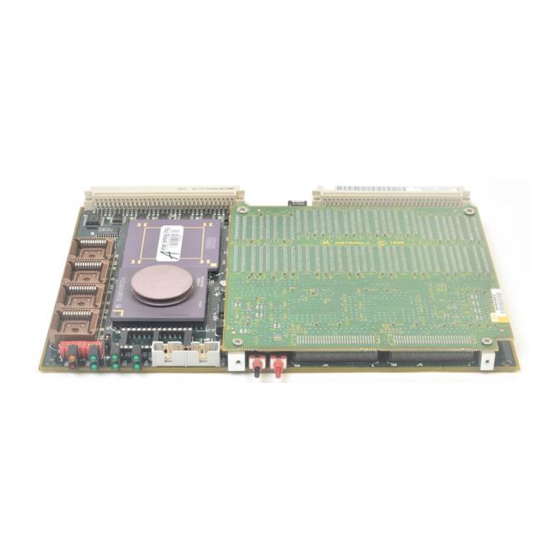
General Information Features Features of the MVME167 are listed below. MC68040 Microprocessor at 25 MHz (-00X models), or 33 MHz (-03X models) 4/8/16/32/64MB of 32-bit DRAM with parity protection or 4/8/16/32/64/128/256MB of DRAM with ECC protection Four 44-pin PLCC ROM sockets (organized as two banks of 32 bits) -
Page 13: Specifications
Specifications Specifications General specifications for the MVME167 are listed in Table 1-2. MVME167 Specifications on page 1-4. The following sections detail cooling requirements and FCC compliance. Cooling Requirements The Motorola MVME167 VMEmodule is specified, designed, and tested to operate reliably with an incoming air temperature range from 0° to 55° C (32°... -
Page 14: Fcc Compliance
Thickness 0.80 inches (20.32 mm) FCC Compliance The MVME167 was tested in an FCC-compliant chassis, and meets the requirements for Class A equipment. FCC compliance was achieved under the following conditions: Shielded cables on all external I/O ports. Cable shields connected to earth ground via metal shell connectors bonded to a conductive module front panel. -
Page 15: General Description
VMEbus master/slave interface, 128KB of static RAM (with optional battery backup), and VMEbus system controller. The I/O on the MVME167 is connected to the VMEbus P2 connector. The main board is connected through a P2 transition board and cables to the transition boards. The... -
Page 16: Equipment Required
General Information Equipment Required The following equipment is required to make a complete system using the MVME167: Terminal Disk drives and controllers Transition module MVME712-12, MVME712-13, MVME712M, MVME712A, MVME712AM, or MVME712B, and connecting cables and P2 adapter Operating system The MVME167Bug debug monitor firmware (167Bug) is provided in two of the four EPROM sockets on the MVME167 main module. -
Page 17: Related Documentation
Related Documentation Related Documentation The following publications are applicable to the MVME167 and may provide additional helpful information. If not shipped with this product, they may be purchased by contacting your local Motorola sales office. Non-Motorola documents may be purchased from the sources listed. -
Page 18: Support Information
Support Information The SIMVME167 manual contains the connector interconnect signal information, parts lists, and the schematics for the MVME167. This manual may be obtained free of charge by contacting your local Motorola sales office. MVME167 Single Board Computer User’s Manual... -
Page 19: Manual Terminology
A byte is eight bits, numbered 0 through 7, with bit 0 being the least significant. A word is 16 bits, numbered 0 through 15, with bit 0 being the least significant. A longword is 32 bits, numbered 0 through 31, with bit 0 being the least significant. MVME167/D3... - Page 20 General Information 1-10 MVME167 Single Board Computer User’s Manual...
-
Page 21: Hardware Preparation And Installation
Some options can not be done in software, so are done by jumpers on headers. Most other modifications are done by setting bits in control registers after the MVME167 has been installed in a system. (The MVME167 registers are described in Chapter 4, and/or in the MVME166/MVME167/MVME187 Single Board Computers Programmer’s Reference... -
Page 22: General Purpose Readable Jumpers On Header J1
SRAM backup power source select (J8) (optional) General Purpose Readable Jumpers on Header J1 Each MVME167 may be configured with readable jumpers. These jumpers can be read as a register (at $FFF40088) in the VMEchip2 LCSR. The bit values are read as a one when the jumper is off, and as a zero when the jumper is on. -
Page 23: Figure 2-1. Mvme167 Switches, Headers, Connectors, Fuses, And Leds
Hardware Preparation MVME FAIL HALT RUN SCON +12V SCSI VME ABORT RESET Figure 2-1. MVME167 Switches, Headers, Connectors, Fuses, and LEDs MVME167/D3... -
Page 24: Serial Port 4 Clock Configuration Select Headers J6 And J7
Serial port 4 can be configured to use clock signals provided by the RTXC4 and TRXC4 signal lines. Headers J6 and J7 on the MVME167 configure serial port 4 to drive or receive RTXC4 and TRXC4, respectively. Factory configuration is with port 4 set to receive both signals. -
Page 25: Sram Backup Power Source Select Header J8
SRAM Backup Power Source Select Header J8 Header J8 is an optional header that is used to select the power source used to back up the SRAM on the MVME167, if the optional battery and circuitry is present. Backup Power Disabled... -
Page 26: Installation Instructions
P1 and P2. It may be installed in any double-height unused card slot, if it is not configured as system controller. If the MVME167 is configured as system controller, it must be installed in the leftmost card slot (slot 1) to correctly initiate the bus-grant daisy-chain and to have proper operation of the IACK-daisy-chain driver. -
Page 27: System Considerations
Connect power cable to ac power source and turn equipment power ON. System Considerations The MVME167 needs to draw power from both P1 and P2 of the VMEbus backplane. P2 is also used for the upper 16 bits of data for 32-bit transfers, and for the upper 8 address lines for extended addressing mode. - Page 28 The MVME167 provides +12 Vdc power to the Ethernet LAN transceiver interface through a 1 amp fuse F2 located on the MVME167 module. The +12V LED lights when +12 Vdc is available. The fuse is socketed, and located near diode CR1. If the Ethernet transceiver fails to operate, check the fuse.
-
Page 29: Operating Instructions
OPERATING INSTRUCTIONS Introduction This chapter provides necessary information to use the MVME167 module in a system configuration. This includes controls and indicators, memory maps, and software initialization of the module. Controls and Indicators The MVME167 module has ABORT and RESET switches; and FAIL, STAT, RUN, SCON, LAN,+12V (LAN power), SCSI, and VME indicators;... - Page 30 The green RUN LED (part of DS2) lights when the local bus TIP* signal line is low. This indicates one of the local bus masters is executing a local bus cycle. The green SCON LED (part of DS2) lights when the VMEchip2 in the MVME167 is the VMEbus system controller.
-
Page 31: Memory Maps
The memory map of devices that respond to the normal address range is shown in the following tables. The normal address range is defined by the Transfer Type (TT) signals on the local bus. On the MVME167, Transfer Types 0, 1, and 2 define the normal address range. -
Page 32: Table 3-1. Local Bus Memory Map
4. Cache inhibit depends on devices in area mapped. 5. This area is not decoded. If these locations are accessed and the local bus timer is enabled, the cycle times out and is terminated by a TEA signal. MVME167 Single Board Computer User’s Manual... -
Page 33: Table 3-2. Local I/O Devices Memory Map
For a more detailed memory map refer to the following detailed peripheral device memory maps. 2. On the MVME167 this area does not return an acknowledge signal. If the local bus timer is enabled, the access times out and is terminated by a TEA signal. -
Page 34: Detailed I/O Memory Maps
8. Port commands to the 82596CA must be written as two 16-bit writes: upper word first and lower word second. 9. The CD2401 appears repeatedly from $FFF45200 to $FFF45FFF on the MVME167. If the local bus timer is enabled, the access times out and is terminated by a TEA signal. Detailed I/O Memory Maps... - Page 35 Memory Maps This page intentionally left blank. MVME167/D3...
-
Page 36: Table 3-3. Vmechip2 Memory Map (Sheet 1 Of 3)
BOARD SELECT WAIT DMA TB SRAM ZERO SNP MODE SPEED DMA CONTROLLER DMA CONTROLLER DMA CONTROLLER DMA CONTROLLER TICK TICK VMEBUS IRQ 1 STAT VMEBUS INTERRUPT VECTOR INTERRUPT LEVEL This sheet continues on facing page. MVME167 Single Board Computer User’s Manual... - Page 37 MAST MASTER ROBN FAIR VMEBUS HALT FAIR RELM VMEBUS DMA LB SNP MODE LOCAL BUS ADDRESS COUNTER VMEBUS ADDRESS COUNTER BYTE COUNTER TABLE ADDRESS COUNTER DMA TABLE DONE INTERRUPT COUNT STAT 1360 9403 This sheet begins on facing page. MVME167/D3...
- Page 38 VME IRQ 6 VME IRQ 5 IRQ LEVEL IRQ LEVEL IRQ LEVEL IRQ LEVEL ABORT VECTOR BASE VECTOR BASE FAIL FAIL GPIOEN REGISTER 0 REGISTER 1 LEVEL LEVEL LEVEL This sheet continues on facing page. 3-10 MVME167 Single Board Computer User’s Manual...
- Page 39 IRQ LEVEL IRQ LEVEL VME IRQ 4 VMEB IRQ 3 VME IRQ 2 VME IRQ 1 IRQ LEVEL IRQ LEVEL IRQ LEVEL IRQ LEVEL GPIOO GPIOI EROM SRAM BSYT BBSY 1361 9403 This sheet begins on facing page. MVME167/D3 3-11...
- Page 40 Operating Instructions This page intentionally left blank. 3-12 MVME167 Single Board Computer User’s Manual...
- Page 41 GENERAL PURPOSE CONTROL AND STATUS REGISTER 0 GENERAL PURPOSE CONTROL AND STATUS REGISTER 1 GENERAL PURPOSE CONTROL AND STATUS REGISTER 2 GENERAL PURPOSE CONTROL AND STATUS REGISTER 3 GENERAL PURPOSE CONTROL AND STATUS REGISTER 4 GENERAL PURPOSE CONTROL AND STATUS REGISTER 5 MVME167/D3 3-13...
-
Page 42: Table 3-4. Pccchip2 Memory Map
IRQ LEVEL PLTY E/L* ICLR PLTY E/L* ICLR PRTR PRTR PRTR PRTR PRTR PRTR BSY IRQ LEVEL PLTY E/L* ICLR CHIP SPEED SCC PROVIDES ITS OWN VECTORS This sheet continues on facing page. 3-14 MVME167 Single Board Computer User’s Manual... - Page 43 IRQ LEVEL PLTY E/L* ICLR PLTY E/L* ICLR PRTR PRTR PRTR PRTR PRTR PRTR PRTR PRTR PRTR PRTR PRTR FAST ENBL ASTB PRINTER DATA INTERRUPT INTERRUPT IPL LEVEL MASK LEVEL 1362 9403 This sheet begins on facing page. MVME167/D3 3-15...
-
Page 44: Table 3-5. Printer Memory Map
Printer BUSY Interrupt Control Register $FFF42034 NAME PLTY E/L* ICLR Printer Input Status Register $FFF42036 NAME PLTY Printer Port Control Register $FFF42037 NAME DOEN FAST Printer Data Register 16 bits $FFF4203A 15-0 NAME PD15 - PD0 3-16 MVME167 Single Board Computer User’s Manual... -
Page 45: Table 3-6. Memc040 Internal Register Memory Map
FSTRD 1 MSIZ2 MSIZ1 MSIZ0 DUMMY 0 DUMMY 1 BASE ADDRESS BAD31 BAD30 BAD29 BAD28 BAD27 BAD26 BAD25 BAD24 DRAM CONTROL BAD23 BAD22 RWB5 SWAIT RWB3 NCEIEN NCEBEN RAMEN BCLK FREQUENCY BCK7 BCK6 BCK5 BCK4 BCK3 BCK2 BCK1 BCK0 MVME167/D3 3-17... - Page 46 EA18 EA17 EA16 ERROR ADDRESS EA15 EA14 EA13 EA12 EA11 EA10 ERROR ADDRESS ERROR SYNDROME DEFAULTS1 WRHDIS STATCOL FSTRD SELI1 SELI0 RSIZ2 RSIZ1 RSIZ0 DEFAULTS2 FRC_OPN XY_FLIP REFDIS TVECT NOCACHE RESST2 RESST1 RESST0 3-18 MVME167 Single Board Computer User’s Manual...
-
Page 47: Table 3-8. Cirrus Logic Cd2401 Serial Port Memory Map
R/W Sync Receive Frame Address Register4 RFAR4 R/W Sync CRC Polynomial Select Register CPSR R/W Sync Receive Baud Rate Period Register RBPR Receive Clock Option Register RCOR Transmit Baud Rate Period Register TBPR Transmit Clock Option Register TCOR MVME167/D3 3-19... - Page 48 Receive End Of Interrupt Register REOIR Transmit Interrupt Registers Transmit Priority Interrupt Level Register TPILR Transmit Interrupt Register Transmit Interrupt Status Register TISR Transmit FIFO Transfer Count TFTC Transmit Data Register Transmit End Of Interrupt Register TEOIR 3-20 MVME167 Single Board Computer User’s Manual...
- Page 49 B Transmit Buffer Address Upper BTBADRU A Transmit Buffer Byte Count ATBCNT B Transmit Buffer Byte Count BTBCNT A Transmit Buffer Status ATBSTS B Transmit Buffer Status BTBSTS Transmit Current Buffer Address Lower TCBADRL Transmit Current Buffer Address Upper TCBADRU MVME167/D3 3-21...
- Page 50 General Timer 1 R Sync General Timer 1 low GT1l R Sync General Timer 1 high GT1h R Sync General Timer 2 R Sync Transmit Timer Register R Async NOTE: This is a 16-bit register. 3-22 MVME167 Single Board Computer User’s Manual...
-
Page 51: Table 3-9. 82596Ca Ethernet Lan Memory Map
$FFF46004 MPU Channel Attention (CA) NOTES: 1. Refer to the MPU Port and MPU Channel Attention registers in the MVME166/MVME167/MVME187 Single Board Computers Programmer’s Reference Guide. 2. After resetting, you must write the System Configuration Pointer to the command registers before writing to the MPU Channel Attention register. Writes to the System Configuration Pointer must be upper word first, lower word second. -
Page 52: Table 3-10. 53C710 Scsi Memory Map
SSTAT0 DSTAT CTEST3 CTEST2 CTEST1 CTEST0 CTEST7 CTEST6 CTEST5 CTEST4 TEMP LCRC CTEST8 ISTAT DFIFO DCMD DNAD DSPS SCRATCH DCNTL DIEN DMODE ADDER NOTE: Accesses may be 8-bit or 32-bit, but not 16-bit. 3-24 MVME167 Single Board Computer User’s Manual... -
Page 53: Table 3-11. Mk48T08 Bbram,Tod Clock Memory Map
System ID $FFFC1F3E - $FFFC1F45 Mezz. Board 1 PWB $FFFC1F46 - $FFFC1F4D Mezz. Board 1 Serial Number $FFFC1F4E - $FFFC1F55 Mezz. Board 2 PWB $FFFC1F56 - $FFFC1F5D Mezz. Board 2 Serial Number $FFFC1F5E - $FFFC1FF6 Reserved $FFFC1FF7 Checksum MVME167/D3 3-25... -
Page 54: Bbram,Tod Clock Memory Map
(TOD) clock, is defined by the chip hardware. The first area is reserved for user data. The second area is used by Motorola networking software. The third area is used by the SYSTEM V/68 operating system. The fourth area is used by the MVME167 board debugger (MVME167Bug). - Page 55 000000470476 Sixteen bytes are reserved for the board ID in ASCII format. For example, for a 16 MB, 25 MHz MVME167 board, this field contains: MVME167-003B (The 12 characters are followed by four blanks.) Sixteen bytes are reserved for the printed wiring assembly (PWA) number assigned to this board in ASCII format.
-
Page 56: Interrupt Acknowledge Map
15. The final one byte of the area is reserved for a checksum (as defined in the MVME167Bug Debugging Package User’s Manual and the Debugging Package for Motorola 68K CISC CPUs User’s Manual) for security and data integrity of the configuration area of the NVRAM. This data is stored in hexadecimal format. -
Page 57: Vmebus Short I/O Memory Map
Memory Maps VMEbus Short I/O Memory Map The VMEchip2 includes a user-programmable map decoder for the GCSR. The GCSR map decoder allows you to program the starting address of the GCSR in the VMEbus short I/O space. MVME167/D3 3-29... -
Page 58: Software Initialization
Any VMEbus access to the MVME167 while it is in the reset state is ignored. If a global bus timer is enabled, a bus error is generated. -
Page 59: Functional Description
Data Bus Structure The local data bus on the MVME167 is a 32-bit synchronous bus that is based on the MC68040 bus, and supports burst transfers and snooping. The various local bus master and slave devices use the local bus to communicate. The local bus is arbitrated by... -
Page 60: Mc68040 Mpu
Dallas DS1210S. Only one backup power source is supported on the MVME167. Each time the MVME167 is powered, the DS1210S checks power source and if the voltage of the backup source is less than two volts, the second memory cycle is blocked. -
Page 61: Onboard Dram
To remove the battery from the module, carefully pull the battery from the socket. Onboard DRAM The MVME167 onboard DRAM is located on a mezzanine board. The mezzanine boards are available in different sizes and with parity protection or ECC protection. -
Page 62: Battery Backed Up Ram And Clock
RAM. Battery Backed Up RAM and Clock The MK48T08 RAM and clock chip is used on the MVME167. This chip provides a time of day clock, oscillator, crystal, power fail detection, memory write protection, 8KB of RAM, and a battery in one 28-pin package. -
Page 63: Parallel Port Interface
MVME712X should be used to convert the I/O connector pinout to industry-standard connectors. The MVME167 board hardware ties the DTR signal from the CD2401 to the pin labeled RTS at connector P2. Likewise, RTS from the CD2401 is tied to DTR on P2. Therefore, when programming the CD2401, assert DTR when you want RTS, and RTS when you want DTR. -
Page 64: Ethernet Interface
If the data in the BBRAM is lost, the user should use the number on the VMEbus P2 connector label to restore it. The Ethernet transceiver interface is located on the MVME167 main module, and the industry standard connector is located on the MVME712X transition module. -
Page 65: Scsi Termination
The system configurer must ensure that the SCSI bus is properly terminated at both ends. On the MVME167, sockets are provided for the terminators on the P2 transition board. If the SCSI bus ends at the P2 transition board, then termination resistors must be installed on the P2 transition board. -
Page 66: Timing Performance
Computers Programmer’s Reference Guide. SCSI Transfers The MVME167 includes a SCSI mass storage bus interface with DMA controller. The SCSI DMA controller uses a FIFO buffer to interface the 8-bit SCSI bus to the 32-bit local bus. The FIFO buffer allows the SCSI DMA controller to efficiently transfer data to the local bus in four longword bursts. -
Page 67: Lan Dma Transfers
The remote status and control connector, J3, is a 20-pin connector located behind the front panel of the MVME167. It provides system designers the flexibility to access critical indicator and reset functions. This allows a system designer to construct a RESET/LED panel that can be located remotely from the MVME167. -
Page 68: Figure 4-1. Mvme167 Main Module Block Diagram
SHEET 12 SHEETS 13-15 SHEET 10 SHEET 5 SHEET 20 SRAMS AND BATTERY/BACKUP EPROMS LEDS AND SHEET 28 SHEETS 16-17 SWITCHES SHEET 9 REMOTE RESET/ABORT/LEDS 1473 9405 Figure 4-1. MVME167 Main Module Block Diagram 4-10 MVME167 Single Board Computer User’s Manual... -
Page 69: Figure 4-2. Parity Dram Mezzanine Module Block Diagram
MVME167 Functional Description ADDRESS MUX MULTIPLEXED ADDRESS SHEET 7 MEMORY ARRAY RDA BUS BANK A SHEET 8 MEMORY ARRAY CONNECTOR ADDRESS BUS RDB BUS BANK B SHEET 5 SHEET 9 MEMORY ARRAY DATA MUX CONNECTORS DATA BUS RDC BUS BANK C... -
Page 70: Figure 4-3. Ecc Dram Mezzanine Module Block Diagram
Functional Description Figure 4-3. ECC DRAM Mezzanine Module Block Diagram 4-12 MVME167 Single Board Computer User’s Manual... -
Page 71: Introduction
Signal levels must lie between +3 and +15 volts for a high level, and between -3 and -15 volts for a low level. Connecting units in parallel may produce out-of-range voltages and is contrary to EIA-232-D specifications. MVME167/D3A-1... -
Page 72: Table A-1. Eia-232-D Interconnections
NOTES: 1. A high EIA-232-D signal level is +3 to +15 volts. A low level is -3 to -15 volts. Connecting units in parallel may produce out-of-range voltages and is contrary to specifications. MVME167 Single Board Computer User’s Manual... -
Page 73: Levels Of Implementation
The DTR signal is sometimes used to disconnect the phone circuit in preparation for another automatic call. It is necessary to provide these signals in order to talk to all possible modems (see Figure A-1). MVME167/D3... -
Page 74: Sample Configurations
+12V LS08 TERMINAL OPTIONAL HARDWARE TRANSPARENT SIG GND MODE CHASSIS GND LOGIC LS08 +12V SIG GND 6850 CONNECTOR -12V MODEM HOST SYSTEM +12V -12V +12V -12V MODULE cb181 9210 Figure A-1. Middle-of-the-Road EIA-232-D Configuration MVME167 Single Board Computer User’s Manual... -
Page 75: Figure A-2. Minimum Eia-232-D Connection
In addition, the TX and RX lines may have to be crossed since TX from a terminal is outgoing but the TX line on a modem is an incoming signal. EIA-232-D CONNECTOR Figure A-2. Minimum EIA-232-D Connection MVME167/D3... -
Page 76: Proper Grounding
CHASSIS GROUND at one point; if several terminals are used with one computer, the logical place for that point is at the computer. The terminals should not have a connection between the logic ground return and the chassis. MVME167 Single Board Computer User’s Manual... - Page 77 MVME167Bug) 1-6, 2-2, 2-6, 3-1, ECC DRAM mezzanine module 4-13 3-30 MVME167 main module 4-11 53C710 (see SCSI Controller) 4-7 parity DRAM mezzanine module 53C710 SCSI memory map 3-24 4-12 82596CA (see Ethernet and LAN) 4-6...
- Page 78 Ethernet address 3-27, 3-28 Ethernet interface 4-6 I/O interfaces 4-5 Ethernet station address 4-6 IACK (interrupt acknowledge) 2-7 Ethernet transceiver interface 4-6 installation instructions 2-6 extended addressing 2-7 interrupt acknowledge (IACK) 2-7 interrupt acknowledge map 3-28 IN-2 MVME167 Single Board Computer User’s Manual...
- Page 79 MK48T08 (see Battery Backed Up RAM, local resources 4-7 BBRAM, and NVRAM) 4-4 local SCSI ID 3-28 MK48T08 BBRAM,TOD Clock memory location monitors 2-8 map 3-25 longword 1-9 model designations 1-1 LRST (local reset) 3-1, 3-30 modem(s) A-1 MVME167/D3 IN-3...
- Page 80 P2 adapter board 1-5, 2-7, 2-8 serial port 4 2-4 parallel port interface 4-6 serial port 4 clock configuration select parallel printer port 4-6 headers J6 and J7 2-4 serial port interface 4-5 IN-4 MVME167 Single Board Computer User’s Manual...
- Page 81 ID 3-28 terminal(s) A-1 terminology 1-9 tick timers 4-7 timeout 4-8 global bus 2-8 local bus 4-8 timers 4-7 timing performance 4-8 TOD clock memory map 3-26 transfer type (TT) signals 3-3 transition modules 1-5, 4-5 transparent mode A-4 MVME167/D3 IN-5...
- Page 82 Index IN-6 MVME167 Single Board Computer User’s Manual...