Table of Contents
Advertisement
Quick Links
SONY.
DIGITAL AUDIO PROCESSOR
PCM-1630
• • • • • •
~..
1111
.clllllllllltr..
• • • • • •
. . .
• •
• ., .. - • • • • •
· · - - - . . .
- - · · · -
Jllll.
• •
II
II
1111
Ill
1111
Mllllll
Bll
II
II
1111
II
111111
1111
111''111
1111
11
11
111
11
• • • •
1111
~•r
111~
1111
II
II
118
II
II
1111
••••II•
1!111
··---·· .. ··---·· .. j······· ·····
IIIII
III'
1111
'11111111111'
1111 ..111r
••• 1111111111
OPERATION AND MAINTENANCE MANUAL
1st Edition (Revised 7)
Serial No. 10001 and Higher
Advertisement
Table of Contents

Related Manuals for Sony PCM-1630


Summary of Contents for Sony PCM-1630
- Page 1 SONY. DIGITAL AUDIO PROCESSOR PCM-1630 • • • • • • 1111 .clllllllllltr.. • • • • • • . . . • • • ., .. - • • • • • · · - - - . . .
- Page 2 Record the serial number in the space provid- i*.;'f~) I::~Vi~l3a1T:;;f:7=..:z.7!t..-~1'£ffl9~.=:.1:: 1'F, ed below. ~~li:.L19 Refer to them whenever you call upon an authorized Sony representative regarding this product. Model No. PCM-1630 Serial No. The material contained in this manual consists of infor-...
- Page 3 1-7-6. Recording and Playback of the SMPTE l-27(F) PCM-1630 ..Time Code ....l-27(E) 1-7-6. Enregistrement et lecture du code de 1-8.
-
Page 4: Table Of Contents
SERVICE INFORMATION SEMICONDUCTOR ASSIGNMENTS Diode ......A-1 2-1. Repacking ......2-1 Transistor . - Page 5 SECTION 1 OPERATION The PCM-1630 is a digital audio processor Emphasis circuitry for professional use, designed to be used The built-in emphasis circuit improves the with a Sony BVU-800DA/800DB videocassette signal-to-noise ratio of high frequencies recorder, a DMR-2000/4000 digital master by raising their recording level and lowering their playback level.
- Page 6 (0 dBs 0.775 V rms) digital audio recorder which has a Analog outputs ANALOG OUTPUT read-after-read function (such as a Sony CH-1 (D-0) /CH-2: DMR-4000 digital master recorder), the Cannon XLR-3-32 type, playback has very high reliability. balanced/unbalanced...
- Page 7 60 IRE) ~lO% BVH-1100, BVH-llOOA COMPOSITE DIGITAL A/B: Recommended editing system 8-pin multi- For elementary edit: connectors, PCM-1630 and two 75 ohms unbalanced DMR-4000s 0.714 Vp-p (data For precise edit: level 60 IRE) ~10% PCM-1630, DAE-1100 or Composite sync inputs DA.E-llOOA, and two...
- Page 8 Accessories supplied DMR-2000 digital master recorder Extension board EX-71 This unit is designed to be used with the PCM-1630 digital audio processor to record and play back digital-quality, Rack mount adaptor high-fidelity sound. When a DAE-1100/llOOA set) Connection cables with...
- Page 9 1-4-3. On Operating Temperature Range l-4-6. On Composite Digital (Video) Inputs DAE-1100/llOOA digital audio editor and Outputs This unit is used with a PCM-1630 digital 1-4-1. On Power Supply Do not install the unit in a location near audio processor and a BVU-BOODB or...
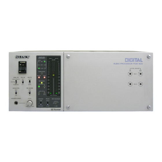
- Page 10 ® A: The composite digital A input (input to ENC IN (encoder input) selector 1-5. LOCATION AND FUNCTION OF PARTS AND CONTROLS the COMPOSITE DIGITAL INPUT A or COMPOSITE Selects a source signal to the built-in DIGITAL A connector) is selected as a 1-5-1.
-
Page 11: Ad-23 Board
~ REF (reference) MARKER selector indication mode selector. This selector sets the reference signal The scale of the level meter can be level within a range of -10 dB to -20 dB in enlarged with the SCALE selector for easy 2-dB steps. - Page 12 1-5-2. Connector Panel ANALOG connectors WORD SYNC connectors COMPOSITE SYNC connectors and 75-ohm termination switch STATUS output connector Ground terminal DIGITAL I/O connectors ® COMPOSITE DIGITAL connectors "--' AC IN connector (BNC type) COMPOSITE DIGITAL connectors (8-pin)----_j VOLTAGE SELECTOR Pin assignment of INPUT and OUTPUT (})ANALOG connectors (equivalent to Cannon connectors...
- Page 13 QD~Ac IN (input) connector @WORD SYNC connectors (BNC type) Connect to an ac outlet using the supplied A word sync signal of 44.1 kHz or 44.056 ac power cord. kHz is input to the WORD SYNC INPUT connector or output from the WORD SYNC OUTPUT connector.
- Page 14 ®DIGITAL I/0 (input/output) connectors 1-5-3. Printed Circuit Boards (BNC type) AD OUT (analog-to-digital output): AID The printed circuit boards are installed converted signals are output from these behind the right front panel. To adjust connectors. the controls and switches on the printed ENC IN (encoder input): Input signals to circuit boards, take off the right front the built-in encoder are supplied to these...
- Page 15 A0-23 board Emphasis identification bits The setting of the EMP switch does not affect the emphasis identification bits in the output signal data when the ENC IN selector on the front panel is set to a particular position, as shown in the following table.
-
Page 16: Enc-2 Board
ENC-2 board The de-emphasis circuit for playback is activated (ON) or deactivated (OFF), depending upon the setting of the DA IN selector as shown below. DA IN ON/OFF status of the selector de-emphasis* ON/OFF status of the em ph a sis identification bits in the signal data input to the COMPOSITE DIGITAL... -
Page 17: Sif-1 Board
SIF-1 board DEC-15 board LED indicators SHl: FS (sampling frequency) selector @sw3 This switch selects the sampling frequency when the unit operates in the internal sync This DIP switch is provided to check the mode: functions of the unit. The switch is factory preset as follows: 44.1 kHz (upper position) 44.056 kHz (lower position) The selected sampling frequency is... - Page 18 The muting time can be set with switches G)swl: M-SENS (muting sensitivity) switch No. 1 to No. 3 as follows. The adjustable This DIP switch adjusts the sensitivity of range is from 1/60 seconds to approximately the muting circuit. That is, it determines how quickly the muting circuit activates 2 seconds.
-
Page 19: Mt-16 Board
MT-16 board SW2 for channel for channel 2: Overload indication adjustment switches These DIP switches set the number of words 3 SW4 of full-scale signals (overload signals) continuously input to the unit, which are indicated with the OVER level indicator on the level meter. - Page 20 1-6-3. Level Adjustment 1-6. RECORDING LEVEL ADJUSTMENT While observing the level meter, adjust the 1-6-1. Reference Signal Level and Headroom signal level as follows. Be sure to set the PEAK indication mode selector to AUTO Headroom means the difference between the when adjusting the level.
- Page 21 8-pin multi-cable ( In this and a recorder for recording) are used in on the PCM-1630 to B, without changing the An example of a basic connection for case, do not make connections the system, a tape can be duplicated connections.
- Page 22 BNC type to BNC type is possible. For details, refer to the operation and maintenance manual of the DAE-1100. PCM-1630 Setting of the selectors ENC IN selector: DIGITAL DA IN selector: EXT PB MODE selector: A <1111~&-----...
- Page 23 DMR-4000 digi~al master recorder. PB MODE selector: A RAW switch (on the DABK-1630): EDT For details, refer to the operation and maintenance manuals of the connected equipment. PCM-1630 DABK-1630 ~ ~~~~~~~~m~~III !!~~~~~'~:;~~'Y'"' ~ ___________ ~---------.to a printer Connecting cables ------ 25-pin to 25-pin ~~r~ ~~[§~C...
- Page 24 1-7-5. Synchronization with Two PCM-1630s PCM-1630 to the COMPOSITE SYNC INPUT connector of the other (connection®) • Four-channel recording and playback is For synchronized playback, record the time possible using two recorders and two code on audio channel-2 track of the tape PCM-1630s.
- Page 25 PCM-1630 to ANALOG and the REC MUTE switch When a DMR-2000/4000 recorder which on the ENC-2 board of the PCM-1630 to ON. incorporates a time code generator is used for A muting signal containing sampling recording, the time code is automatically...
- Page 26 I. Ut-'t:.tif-\ IIUI\l ,1,;,:.1::::111 (OI OPTION) REC. SECTION :>'1 DIGITAL (AD) OUT lDIGITALf g~~t DIGITAL (DEC) OUT ANALOG ENC IN V~OEO :REC LEVEL ANALOG DIGITAL'\ INPUT :1/ ___ : rr- }COMPOSITE ~ENCODER CH-2 DUBBING DIGITAL OUTPUT L _____________________ f--E:~:~~I: ,.1. MUTE ______ SE~C~T~I~O~N--------------------------~...
- Page 27 1-9. SIGNAL FLOW 1-9-1. Data Flow AD DT (25) ANALOG INPUT COMPOSITE (32) DIGITAL ENC IN OUTPUT ANALOG/DIGITAL (ENC IN) (25) COMPOSITE DIGITAL INPUT METER REC/PB: (MONITOR): -+----------+:----{ ANALOG OUTPUT (OUB RAW) ------------------------- __ .. (RAW) (25), (32): Number: of slots Switches ENC IN selector:: ANALOG/DIGITAL/DUBBING DA IN selector:: !NT/EXT...
- Page 28 1-10. SIGNAL FORMAT 1-10-1. Composite Digital (Video) Input/Output Signals Data configuration : . - - - - - - - - - - - - - 1 7 - - - - - - - - - - - - t - - -245 H - ..
- Page 29 1-10-2. Digital Input/Output and Control Signals Digital input/output format 22.676 (44.1 kHz) 22.698 i-------------(44.056kHz)-------------~ Word sync CH-1 data CH-2 data 29th !when the bit is 0 :When the 29th bit is PCM data !Sync information Control bits or :area user's bits Block flag bit 3 4 5 6 7 8 9 10 11 12 13 14 15 16 17 18 19 20 21 22 23 24 25 26 27 28 29...
- Page 30 00: Emphasis is not used. identification bits are also "0". 01: Emphasis is used. ** In the PCM-1630, the dubbing prohibition (50 rsec., 15 rsec.) bit is always "0". *** For interface (signal: DA IN CH-1) between the DAE-llOOA with serial No.
- Page 31 SYNC PCM-1630 for PCM a recording/playback system consisting of a ® signal PCM-1630 and a recorder is to be synchronized with other equipment (such as COMPOSITE DIGITAL a VTR for recording/playing back video COMPOSITE Recorder signals, or audio equipment), the system...
-
Page 32: Repacking
SECTION 2 SERVICE INFORMATION 2-1. REPACKING POWER CORD: 1 OPERATION & MAINTENANCE CONNECTION CORD: 1 MANUAL: 1 (8-pin multi-cable VMC-3P) CABLE ASSIES: 2 ..-::;;;~:-:;::?' (75-ohm coaxial cables) EX-71 MOUNTED PCB: PCM-1630 (U/C, AEP) -
Page 33: Rack Mounting
Screws, +B 4x12 Inner members 3) Push the PCM-1630 into the rack and secure it to the rack with +RK 5x16 screws and ornamental washers. Max. slide distance 660 mm (when 26" rail used) -
Page 34: Case Removal
2-3. CASE REMOVAL PCM-1630 Meter Panel Removal PCM-1630 (U/C. AEP) -
Page 35: Heat Sink Assy Removal
Rear Ornamental Plate Removal > B 3x5 <1llr;) 2-4. HEAT SINK ASSY REMOVAL Caution: When reinstalling the heat sink assy, first put the harness in the chassis, and then install the heat sink. PCM-1630 (U/C, AEP) - Page 36 When installing the regulators of PS-81 board on the heat sink, do not forget to use an insulating bushing to prevent short circuit between the radiator fms of three regulators (Q4, QS and Q6) and the heat sink. Heat sink +B 2. Insulating bushing PS-81 board PCM-1630 (U/C, AEP)
- Page 37 (6) FREQUENCY COUNTER Hewlet-Packard Model 5315A/OPT003 (7) OSCILLOSCOPE Tektronix Model475A (8) EX-71 EXTENSION BOARD Sony Part No. A-7850-303-A One EX-71 board is supplied with PCM-1630. Heat sink (9) ADJUSTMENT SCREWDRIVER Sony Part No. 7-700-733-01 Insert the EX-71 extension board into each AD-23, DEC-15 and MT-16 board slot.
- Page 38 EX-71 extension board <( ANALOG IN ..J RV1 01 (CH- 1) <( CH-1 or CH-2 AD-23 board RV102 RV103 ANALOG OUT CH-1 or CH-2 ()() LEVEL PCM-1630 ADJUST ..J RV202 RV203 COMPOSITE ()() DIGITAL IN A Distortion RV201 (CH-2) meter COMPOSITE DIGITAL...
- Page 39 Spec.; Less than 0.04% observe the waveform as shown below. 5Jlsec/DIV 0.5V/DIV 8. Tum RV103 (RV203) fully counterclockwise. The base of the waveform at TP103 (TP203) becomes doubly as shown below. This is called as 1st double base. PCM-1630 (UC/AEP)
-
Page 40: Ments (Da-15 Board)
Connect the frequency counter to TP12 on the DA-15 board. Adjust CVl to obtain the following specification. Spec.; 39933.10 ± 0.02 kHz If the beat grates on the ear when the signal is not inputted, fmely adjust CVl. TP120 DA-15 BOARD -component side- PCM-1630 (UC/AEP) -
Page 41: Level Adjustment
Input 16kHz, 14 dBs signal to the ANALOG INPUT CH-1 (CH-2) connector. Adjust RV1 02 (RV202) to obtain the following speci- fication. Spec.; Distortion Less than 0.03% RV102 () RV101 ©@ LEVEL © () RV201 ADJUST RV202 -component side- DA-15 BOARD PCM-1630 (UC/AEP) -
Page 42: Output Offset Adjustment
Short-circuit between COLD and GND of the ANA- LOG OUTPUT CH-1 (CH-2) connector. Check the DC voltage between the above HOT and GND. Adjust RV104 (RV204) to obtain the following speci- fication. Spec.; ±20mV RV103 () RV104 () RV203 () RV204 -component side- DA-15 BOARD PCM-1630 (UC/AEP) -
Page 43: Composite Digital Output And Clock Adjustments (Sif-1 Board)
L ..- - - - - - - ' EX-71 board 3-7-3 Oscilloscope .._ _ _ _ _ _j"_. f=44.051 kHzto44.105kHz EX-71 board Jl.JL PCM-1630 SIF-1 board Standard Signal 1--'----iWORD SYNC IN Generator 3-7-4. Osc iII oscope Switch Settings: Free PCM-1630 (UC/AEP) -
Page 44: Composite Digital Output Level Adjustment
3-5-2. Composite Sync Phase Adjustment Adjust RV2 so that the phase of COMPOSITE SYNC IN (Board Connector No. A-10) coincides with that of the COMPOSITE SYNC OUT (Board Connector No. A-8). TP58 TP11 TP59 SIF-1 BOARD -component side- PCM-1630 (UC/AEP) - Page 45 4. Connect CH-2 to TP14 (DATA extraction level). imate center of the DATA region. For all of the above, connect the GND of CH-1 to EPl, and the GND of CH-2 to EP2. IBBBBI TP11 TP10 0TP12 RV1 () TP14 TP13 DEC-15 BOARD -component side- PCM-1630 (UC/AEP)
-
Page 46: Diode
DIODE, TRANSISTO SECTION A SEMICONDUCTOR PIN ASSIGNMENTS ICs, transistors and diodes whoses functions are equivalent are described here. Therefore, incompatible device names may be described together. For parts replacement, refer to the Replaceable Parts section in this manual. 2SAT220A DTC143TF (R = 4.7k) BG5534S PR3432S 2SB649A... - Page 47 TRANSISTOR 2SK118 2SC2690A 2SD669A 2SK752 2SC2785 2SK523 :il' l ii 'Ill _;j~ti --, 2SC2855 2SK110 25084 2SJ74...
- Page 48 AM26LS31 PC (ADVANCED MICRO DEVICE) CX-7738 (SONY) HIGH SPEED DIFFERENTIAL UNE DRIVER C·MOS SYNC GENERATOR (NTSC) -TOP VIEW- -TOP VIEW- FUNCTION TABLE EN2 EN1 OUTPUT ENABLE FH OUT ENABLE Ht-Z CK IN ENABLE LOW LEVEL 1 ; HIGH LEVEL HCOMOUT HI-Z;...
- Page 49 NTSC PAL, SEC AM (FIELD '· 3) N:NTSC, PALM P:9.86SpS N:9.S48pS 0/E{Fv/2} LALT - - - - t - - - - - l CF!Fv/4l I NTSCJ CF! Fv/8 !PALM) NTSC (FIELD2,4) NTSC SYNC LALT (PALMll BF I CBLK ( NTSC l 0/E(Fv/2) CF( Fv /4) t NTSC )
- Page 50 CX20018 CSONYI CX7903 (SONY) 16-BIT AID CONVERTER C-MOS GENLOCK DRIVER FOR CX773A -TOP VIEW- -TOPVJEW- I OUT 2 DATA I OUT 1 I SET BCLK Control pin VH 2 tmclk CIN 2 INPUTS EXT LOCK MODE CLK OUT VL 2...
- Page 51 C-MOS HDM1 MODULATOR tCRCC GENERATOR) -TOP VIEW- -TOP VIEW- SCLK ER 10 CRCC ON/OFF LATCH LRCK WCLK BCLK LRCK OUT CX23034 I SONY l C-MOS DIGITAL FILTER FOR OVER-SAMPLING -TOP VIEW- XTAL AMPO TEST 1 COCK LRCK WCLK OOUT DATA TEST 7...
- Page 52 CX23065 (SONY) CX23071 !SONY) N-MOS PHASE COMPARATOR WITH INVERSION AMPLIFIER C-MOS DECODER-A PRINTED SIDE VIEW- -'TOPVIEI'I- " " " ACTIVE OS10 18 HIGH IMPEDANCE 300590 050017 1 ; HIGH LEVEL 0; LOW LEVEL AMP AMP OUT 310600 049016 320610 048015...
- Page 53 CX23073A (SONY) CX23072 (SONY) C-MOS DATA SEPARATOI=I C-MOS OECDOER-8 -TOPVIEto- -TOP VIOl- " RHliOVT 051018 300590 050017 RAVE OUT 310600 049016 ROB OUT 320610 0.118015 ROT ouT 330620 047014 340630 046013 LHL!ouT 350640 045012 LAVE ouT • LOB ouT MUTSour...
- Page 54 CX23074 (SONY) CXOI027P (SONY) C-loiOS SYNC SEPARATOR C-NOS BIT RATE Cllf.IVERTER -TOPVIE\111- -TOP VIEW- SYHCIN PCOTn1 VPLSIN PFISiflN TCSYJN TCOTJN PCLPOIJT CLPFour TCLPOUl OTZHOUT BCKPour SKNBouT VPRTour P8V6our PBVOUT lNTVour VRSTour fiHTour STSCour DINT S't'NOIN VPLS SYNC EINT OINT STSC...
- Page 55 HM6148HP-45 (HITACHI) MC74HC10N (MOTOROLA) C-MOS 4096-BIT (1024x4) STATIC RAM WITH 3·STATE OUTPUT C·MOS 3-INPUT NAND GATE -TOP VIEW- -TOP VIEW- =~=L>-y Y=Aec~A-+B+C A B C Y 0 0 0 1 A91N 0 I 0 1 DO 1/0 D1 110 1 0 1 LOW LEVEL 1 I 1 0 1 :HIGH LEVEL...
- Page 56 MC1648P (MOTOROLA) MC74HC163N (MOTOROLA) C-MOS PRESETTABLE SYNCHRONOUS 4-BIT BINARY COUNTER ECL VOLTAGE CONTROLLED OSCILLATOR -TOP VIEW- -TOP VIEW- COUNT SEQUENCE MODE SELECT ION OUTPUTS CONTROL INPUTS MODE COUNT RESET (SYNCHRONOUS) PRESET !SYNCHRONOUS) NO COUNT NO COUNT MC4044P (MOTOROLA) COUNT PHASE-FREQUENCY DETECTOR -TOP VIEW- CO IS HIGH WHEN EN2 INPUT IS HIGH AND COUNT IS "15':...
- Page 57 NJM4 5600X (JRCl MM5437N IN.S.I NE5532P (TIJ OPERATIONAL AMPLIFIER DIGITAL NOISE SOURCE lOW NOISE OPERATIONAL AMPLIFIER -TOP VIEW- -TOP VIEW- -TOP VIEW- NE5534P (TI) OPERATIONAL AMPLIFIER -TOP VIEW- NJM78 ? ?A (JRC) POSITIVE VOLTAGE REGULATOR {1A) -SIDE VIEW- MSM5128·15RS (OKI)' (ACCESS TIME 150 nS) OUTPUT VOLTAGE...
- Page 58 SN75121 (TI) NJM79M >A (JAC) DUAL LINE DRIVER AND TRIPLE LINE RECEIVER NEGATIVE VOLTAGE REGULATOR (500mA) -TOP VIEW- FRONT VIEW - - 5V NJM79M05A NJM79M06A - 8V NJM79M08A - 9V NJM79M09A -12V NJM79M1 2A -15V NJM79M15A -18V NJM79M1 SA -24V NJM79M24A A ·...
- Page 59 TC40H1 S3P (TOSHIBA) TC40H002P (TOSHIBA) C-MOS 4-UNE-T0-1-UNE DATA SELECTOR/MULTIPLEXER C-MOS 2-INPUT NOR GATE -TOP VIEW- -TOP VIEW- A 8 Y 0 0 1 1 0 0 1 1 0 O:LOW LEVEL 1: HIGH LEVEL TC40H004P (TOSHIBA) C-MOS INVERTER -TOP VIEW- CONTROL IN CHANNEL A-[>-Y...
- Page 60 TC74HCOOP (TOSHIBA) TC40H163P (TOSHIBA) C-MOS 2-INPUT NAND GATE C-MOS PRESETTABLE SYNCHRONOUS 4-BIT BINARY COUNTER -TOP VIEW- -TOP VIEW- ~D-Y=~D-y MODE SELECTION CONT. INPUTS MODE Y= A·B=A+B RD LD Nl EN2 RESET { SYNCHRONOUSJ PRESET LOW LEVEL {SYNCHRONOUS) ~HIGH LEVEL NO COUNT NO COUNT COUNT COUNT SEQUENCE...
- Page 61 TC74HC85P (TOSHIBA) TC74HC27P !TOSHIBA) C MOS 4-BIT MAGNITUDE COMPARATOR C-MOS 3-\NPUT POSITIVE-NOR GATE -TOP VIEW- -TOP VIEW- A< B •· 8· Y=A+B+C CASCADE A= B INPUTS A B c y 0 0 0 1 A> B 0 0 1 0 DATA 0 1 0 0 A>...
- Page 62 TC74HC161 P (TOSHIBA} TC74HC123P (TOSHIBA} C-MOS SYNCHRONOUS PRESEITABLE 4-BIT BINARY COUNTER C-MOS RETRIGGEAABLE MONOSTABLE MULTIVIBRATOR -TOP VIEW- -TOP VIEW- INPUTS OUTPUTS RD A S I L 1 t_ 1.__1" 0; LOW LEVEL 1 ; HIGH LEVEL X; DON'T CARE ~!ENABLE 21tH ~LOAOIIN OUTPUT PULSE WIDTH...
- Page 63 TC74 HC240P (TOSHIBA) TC74HC273P (TOSHIBA) C-MOS 3-STATE INVERTER/LINE DRIVER C-MOS 0-TYPE FLIP· FLOP WITH RESET -TOP VIEW- -TOP VIEW- EACH FLIP- FLOP A-~Y INPUTS HI-Z O;LOW LEVEL t ; HIGH LEVEL 0 ;LOW LEVEL X; DON'T CARE 1 ; HIGH LEVEL HI-Z;HIGH IMPEDANCE X ;...
- Page 64 uPC311 C {NEC) TL072ACP {TI) VOLTAGE COMPARATOR OPERATIONAL AMPLIFIER -TOP VIEW- (LOW·NOISE. JFET-INPUT) -TOP VIEW- ~PC741C NECl OPERATIONAL AMPLIFIER -TOP VIEW- 733DC FSCl DIFFERENTIAL VIDEO AMPLIFIER -TOP VIEW- OFFSET NULL -INPUT +INPUT ~PCB11C (NEC) uA78 11UC (FSC) HIGH STABILITY OPERATIONAL AMPLIFIER POSITIVE VOLTAGE REGULATOR (1 A) 5V JJA7805UC FS7805 )JPC14305H )JPC7805H...
- Page 65 uPC311 C (NEC) TL072ACP (TI) VOLTAGE COMPARATOR OPERATIONAL AMPLIFIER -TOP VIEW- {LOW-NOISE. JFET-INPUT) -TOP VIEW- pPC741C INECI OPERATIONAL AMPLIFIER -TOP VIEW- pA 733DC I FSCI DIFFERENTIAL VIDEO AMPLIFIER -TOP VIEW- OFFSET NULL -INPUT +INPUT ~PC811C INEC) uA78 ?UC (FSC) HIGH STABILITY OPERATIONAL AMPLIFIER POSITIVE VOLTAGE REGULATOR (lA) ~"...
- Page 66 ~PD8749HD I NEC) uPD8243C (NEC) N-MOS 8-BIT MICROCOMPUTER N·MOS 1/0 PORT EXPANDER -TOP VIEW- -TOP VIEW- TEST 0 TEST 1 IN XTAL 1 XTAL 2 RESET PSEN ouT ALE OUT CONTROL AND PORT ADDRESSING PROG PROGRAM PULSE INPUT PORT CONTROL P23 P22 P21 P20 CHIP SELECT INPUT 110 PORT 1...
- Page 67 BLOCK DIAGRAM BLOCK DIAGRAM SECTION 8 BLOCK DIAGRAMS AND CIRCUIT DESCRIPTION PCM-1630...
-
Page 68: Da-15 Board
The monitor signals for headphones go to DA-15 board JJm~~--::.>il• ~ tc~~~ i' ;t LOW tct.r.-? t.: BUFFER CONVERTER through attenuators and headphones amplifiers. :fJ? 31-m~fi btU' J§c7)-t:.::. HEADPHONES f;t;:,.; '""''Y < ~~"'""-h AMP Z.Ji DA -15 AD-23 BOARD LEVEL DIAGRAM PCM-1630... - Page 69 OFF SW NOISE IC15 IC12, 103, 203 ,--<>~ Q1-Q6 SOURCE IC14, 16 AD OFFSET FEED BACK WDGK 1 WDGK CLOCK FIL WDGK BIT GK BCLK SELECTOR CONTROL IITTC'Ki FIL BIT GK IC6, 7 IC2, 3 AD-23 BOARD BLOCK DIAGRAM PCM-1630...
- Page 70 The monitor selector switches between a recording monitor '.Q o MONITOR SELECTOR ii, AD- 23 £~iJ, signal from the AD-23 board and a playback monitor signal DA-15£~(!)~ ~ -~%~-!;] ~ ~:Z. -.ffi% c -c "' from this DA-15 board . DA-15 BOARD LEVEL DIAGRAM PCM-1630...
- Page 71 HEADPHONE BLOCK2 LVL OUT ·• SELECTOR1 AMP1 MON I IC110 IC111 REC/PB MUT I LVL IN 2 MONITOR HEADPHONE REC MON I LVL OUT 2 AMP2 SELECTOR2 REC MON 2 MON 2 IC210 IC211 DA-15 BOARD BLOCK DIAGRAM PCM-1630 B-10...
- Page 72 OA-15 A-15 BLOCK DIAGRAM 1--- f------ IC109, 112, 113 & HA. CC DEGLITCH1 LINE DE-EMPHASIS I .I LEVEL I A OUT 1 (-) ·: LPF1 AMP1 IADJUST11 I AMP1 1 (+) IC101-106 AFL101, IC107 IC108 IC108, 109 EM PB SW IC212, 213, 209 &...
- Page 73 ENC-2 ENC-2 ENC-2 BLOCK DIAGRAM BLOCK DIAGRAM ENC-2£*-&: ENC-2 BOARD On the ENC-2 board 2 channel 25 slot 16 bit digital signals ;vm%~, lli¥51-~U~ 2 CH 1- 16 1- 7:; !::" are subjected to time division multiplexing and crossword '7- l-'~%{t 7.lcf- £{t L -c 35 H (H;...
- Page 74 2K. 3K. 4K. 5K. 5H. 7K. 9H EM REG SW EMPH EM REG EM ID EMPH S EMPH EMPH EM PB SW EM PB ~~--------------~ 7C, BC D~----; INT/EXT SW INT/EXT O""ION OOON ENC-2 BOARD BLOCK DIAGRAM B-13 B-14 PCM-1630...
- Page 75 -rrn-~Q)iffl:h~r~Q) TIMING GENERATOR ffl PLL :to .t rJ WD SYNC GENERA- 4. DIGITAL 1/0 ~;:_ Jv-t ::1 ' / 5. SONY FORMAT DIGITAL 1/0@Ili\!:to .t rJLINE {g~Q)-Jn~;:t Q)f.\LJ!: DRNER (ffi~~~) 6. COMPOSITE SYNC :to .t rJ COMPOSITE DIGITAL DA-15 DA IN...
- Page 76 '------------1~ DIVIDER 5. Sony Format Digital 1/0 Circuit and Line Driver The Sl F-1 board handles the PCM-1630's internal system The digital data from the DA IN connector on the interfacing as well as generation and input/output of the EXTERNAL!
- Page 77 SIF-1 SIF-1 BLOCK DIAGRAM BLOCK DIAGRAM r---------------------------------------------------------------------------, SYNC DUTY ADJ. C SYNC IN EDGE LEVE~r C-MOS SYNC PHASE DETECTOR SELECTOR COMPARATOR TRANSFORMER 4J, 5K G4, 5 48, 3K, 6K EDGE TIMING I W SYNC IN ~~~~~l:t-------~t=§o~ET~E~C~TgoR~t=~~~~~~ MUTING L-----------j1 DIVIDER SIGNAL "j EXTERNAL' 5M, 5L, 6L, 6K...
- Page 78 OEC-15 OEC-15 BLOCK DIAGRAM BLOCK DIAGRAM DEC-15 BOARD DEC-15 M HOLD Receiving the composite digital (video) signal from the ~·- 1v ::t"- ::t" il• I? (J) COMPOSITE :::1 - digital audio recorder, the DEC-15 circuit separates the RAR MUT fl§%~~fl§L-c, DIGITAL (VIDEO) SYNC&LfDATA HOLD...
-
Page 79: Dec-15 Board
CRC S CRC ER DEC/RARI CRC ER A+RAR RAR·BD RtiR RAR EN A+RAR·BO+RAR·BD·RAR-A+RAW MODE DUB RAWS B+RAR·8D·RAR-B+RAW RAR 80 DECODE DUB RAW RAR 8 DUB RAW RAR ON 6D, 7C,8C,8D,8E A ON 8 ON DEC-15 BOARD BLOCK DIAGRAM 8-20 8-21 PCM-1630... - Page 80 (R WDCK, R BIT CK, R DTL R DT2) c L -c STATUS clock and data are sent by the RS-422 driver as remote !l ~ -~~zG.h~o signals (R WDCK, R BITCK, R DT1 and R DT2). to the MT-16 Bl STATUS connector. PCM-1630 B-22 B-23...
- Page 81 MT-16 MT-16 BLOCK DIAGRAM BLOCK DIAGRAM OVER LEVEL DETECTOR PEAK PEAK r - - ""'\ SEQU-,_ ENCE !!."r;.! ,...-- ~..-,..;2L. 4L 3J,4J SCALE L . . . - - - - - - · 1 - - - - - 1 - - - PEAK PEAK hOLD ro--...
- Page 82 AD-23 AD-23 1-616-292-12 1-616-292-12 SECTION C SCHEMATIC AND CIRCUIT BOARD DIAGRAMS AD-23 BOARD (1-616-292-12) S/N; 10001 TO 10800 Component Side &~~(~~..;:~""' ·~~1~·'x ·~' ~.Jt;~o. t>·-.-"~·~·-·--~.~·--·· 1\136 ,· •. - ·~·---·,.~,~~ ~g;;; ~ ·~ ~ZJB , , _ ' , c,-cc ..1::-r-c-,.---:-:-:::---'--_.;:_:, Ciffut:;;...
- Page 83 & AD-23 AD-23 & 1-616-292-13 HIGHER 1-616-292-13 HIGHER 1~801 AD-23 BOARD (1-616-292-13) S/N; AND HIGHER! Component Side Note: TP16 on the AD-23 board has been misprinted. Please read TP16 as TP106. Parts tha: have been added. C30 1 C302...
- Page 84 "' HB26 T P2 E.GND Ill M 54 3 7 ( lC-100 GNO 1 C20 1 II1J3 '" IC-201 IC-202 R 23 R2JJ "' '" 0203~"'' II:HJ "' AD-23 BOARO "' BOARD 1'10.1-616-292-11 HIGHER 100)( PCM-1630 SERIAL N0.10001 r'11gr"1er O.GN02...
- Page 85 DA-1~ DA-15 1-616-293-11 1-616-293-11 OA-15 BOARD (1-616-293-11) S/N: 0, U/C 10001 TO 10204 Component Side S/N; AEP 10001 TO 10126 ,-,'~. ~ - '- ;,~ ~ -~ "-'---'-'---'-----'-----' Traces that have been cut. Jumper that have been soldered. Parts that have been added. RV103 ---- IC112-18 0101-C----C108 0214-S ---- R219...
- Page 86 OA-15 DA-15 1-616-293-12 1-616-293-12 OA-15 BOARD (1-616-293-12) S/N; 0, U/C 10205 TO 10800 Component Side S/N; AEP 10127 TO 10800 EPIO c.:CJ3 s"oN'v MADE IN JAPAN Tr·a:::es tr1ot r,ave besn C~Jt" Jumpe~ that have been soldered. Parts that have been added. 0102-C ---- ClOB R114---C108 R301...
- Page 87 DA-15 DA-15 & 1-616-293-13 & HIGHER 1-616-293-13 HIGHER DA-15 BOARD ( 1-616-293-13) [S/N; 10801 AND HIGHER Component Side Parts that have been added. Applicable Serial Jumpers that have been soldered. C201---- IC1-2 R301 c101---- IC1-15 R302 R303 10801 and higher R304 C301 C302...
- Page 88 DA-15 DA-15 1-616-293-11 1-616-293-11 DA-15 BOARD S/N; 10001 TO 10204 0/A Converter S/N; AEP 10001 TO 10126 PB Audio IC • 1 TP 1 2 0\01 " " lt"·· C\21 i::;:l/50 C\31 0150 IC-14 " .~'~ ~~·~·-8 LID\ 1:::~ I C- 1 0 '-----~'L-/~ OJN2 WOCKI...
- Page 89 1 . . ]-A40 '--1840 ~~·~,----------------------~~---+----r 2(•) f-A38 ~· '--1 A OUT 2(<1 I C- 205 IC-211 4560 DA-15 BOARO BOA.AD ND.l-816-293-11 PCM-1630 {,J, U/C) SERIA.L N0.10001 1020oil PCM-Hi30 (A.EPl SERIA.L N0.10001 10126 *THE CIRCUIT OIAGR.Id', SAME C-10 (a) C-11(a)
- Page 90 DA-15 DA-15 1-616-293-12 1-616-293-12 DA-15 BOARD S/N: U/C 10205 TO 10800 Converter S/N: AEP 10127 TO 10800 Audio (.I..GNDl (.I..GNDJ (.I..GNOJ -22V IC-1 10 GNO) TP 1 2 : : ; 1--g· -+'-""'-~' TT "' Tf "l 1-------'--"' ,,___, •sv l1ooi2sl ' "...
- Page 91 JC-17 LIOI . CX23065 " 2SK I 1 .--t----- TQP9 MCI&48 1411 lOOP lOOP IC-202 1>PC8!! 2(G) DA-15 BOARO SOARD NO. 1-516-293-12 PCM-1630 U/C) SERIAL N0.10205 10800 (..J, PCM-1630 (AEPl SERIAL N0.10127 10800 CIRCUIT DIAGRAM SAME C-10 (b) C-11 (b)
- Page 92 DA...,.15 DA...,.15 & 1-616-293-13 & HIGHER 1-616-293-13 HIGHER OA-15 BOARD SIN; 10801 AND HIGHER Converter Audio (A.GNO) (A,GNOI (A.GNOI IA.GNO) IO.GNOJ r c- to J·"' ' , ' , l7150 100/25 '-----''"''"-0 ---'-"""'-'0 IC-14 IC- 10 HC08 uPC~ -=----d .&.>:201 C~<9 C2JJ: "...
- Page 93 DA-15 DA-15 DA-15 1-616-293-13 & HIGHER & 1-616-293-13 HIGHER IC-l I C- 1 07 I C- I 08 I C- 1 09 IC- I 08 IC-102 1 02 I C- 1 01 C::?DI IOOOP IC-202 " '" uPCBit "':~ ::!::.~"" IC-~C!l!l C20J l'"r"-"05_-----T---+--,-,-.
- Page 94 ENC-2 ENC-2 1-614-294-11 1-614-294-11 (1-616-294-11) S/N; 10001 TO 10204 ENC-2 BOARD ..1, S/N; AEP Component Side 10001 TO 10126 Traces that have been cut. IC1C-3----IC3B-11 IC36-10 ---- IC4C-9 Jumpers that have been scldered. IClC-3 ----IC3B-10 IC3B-11 ---- IC4C-9 C-13 C-14...
- Page 95 ENC-2 ENC-2 & & 1-616-294-12 HIGHER 1-616-294-12 HIGHER (1-616-294-12) S/N; U/C 10205 AND HIGHER ENC-2 BOARD S/N; AEP 10127 AND HIGHER Component Side C-13 (b) C-14 (b)
- Page 96 ENC-2 ENC-2 ENC-2 BOARD Encoder k~~~dAl Ylf-'''---------, R6 I FWOCK v:zr'-------, \~82 ~~~2~AJbHYJf-'---------, k~" Hp'" r-" -----, lJ :: " 5!10 "' 12!1V IS 1 1001( TP 16 T PI 8 l[STJ c• '" c f , ~ " - ' : _ : · _ r = l = = = = : = = ' : = c = : ~ : = , ~ = ; = ' = ' = " ~ ' ~ D "...
- Page 97 ENC-2 HCJf>8 f>~AIO OlM£1 .II., -~ ~LB~o~o~--~'~"'~--- HCI5J 1 AHt:J68 8HCOO TP4 7 t.t':t:t==~'~'j:~:,~"~==j TP1b TP 18 HCJO t-------------'''<11'\: ~~· ~:_,, ~ ~ ~S_J • A 0 A I .>--+-+-- TP15 >--4--+--l--1-1 >-----+--l--1-1 DO~IIJ>-----+--l--1-1 ,---------~----~--+-----~CK4J ~~~~con --------~~t=:t~:t~==~==~~t=====~~ l~~~-~::- HC~~~ TP42 ~i ~~'"...
- Page 98 SIF-1 SIF-1 1-616-295-11 1-616-295-11 BOARD SIF-1 (1-616-295-11) S/N; 0, U/C 10001 TO 10204 Component Side S/N; AEP 10001 TO 10126 Traces that have been cut. Jumpers that have been soldered. Parts that have been added. IC4E-2----GNO IC5F-9----R44 IC6H-1----IC6H-14 C150 IC4E-3----GNO IC2E-1----IC3E-1 IC6H-2----IC6H-3 IC6H...
- Page 99 & SIF-1 1-616-295-12 & HIGHER 1-616-295-12 HIGHER SIF-1 (1-616-295-12) S/N; U/C 10205 AND HIGHER SIF-1 BOARD S/N; AEP 10127 AND HIGHER Component Side A part that has been added. Applicable Serial No. Traces that have been cut. Jumpers that have been soldered. TP56 ---- IC4C-7 IC5F-9----R44 U/C: 10205...
- Page 100 SIF-1 SIF-1 SIF-1 BOARD System Interface \lOCK 2KR Q I '" .------,~=-:-::--,-'-' . : . : . , ' ~ H" =~':j' :~:~:~·~':jlf: ~ ~) ! i j : E C S.,., C~23070 LJ-----+===. : = =====+======--=====h rm:. :l==t=tH= CX23070 ___(_1_4~•j:•...
- Page 101 SIF-1 SIF-1 SIF-1 NOTE: ·The signal line (IC7F-22 to IC4C-11) is applicable to the units with Serial No.11301 and higher. ·The following signal lines and a resistor are applicable to the units with Serial No 12801 and higher. "' C 1 4 7 ICBH-11 IC9F-14 to 843...
- Page 102 DEC-15 DEC-15 DEC-15 BOARD (1-616-296-11) Component Side f;:/~':; ::.J_:;·f;:,- ;; . -~:.: > ~::;,,{"' ,~_.S; ~,'J,:--o\': ·:': ~~ i' \\" t:,t " """"" ;;;:~,~ ~~ ~"''";""'{~,/;fift""< :~:!g~ C · 2 ° B ' ~ ~ : ' w ; ~ t ~ : i ~<...
- Page 103 DEC-15 DEC-15 DEC-15 BOARD (1-616-296-11) Component Side o'o:"c. ,.J~7 Part that has been added. Traces that have been cut. Jumpers that have been soldered. Applicable Serial NO. IC3L 3----- GND ""1Wl 3 10205 and higher -------- IC9K-3----- GND IC3L-4 IC9K-3 -------- IC3L-3 IC9K-27...
- Page 104 DEC-15 DEC-15 DEC-15 BOARD T P3 Decoder TP19 Sync Separator Data Separator Decoder JJJJJJJJJJJJJJJJ u. u J,Y, YJ, TD22 y,?J,ff, Y,.Y, <5 ~~~~::~~:~~~ V> V> " ' ,_., "' " ' " ' ,-.. " ' U U : E < < < < < < < < < < - 0 0 0 0 ~OliN R142 ><...
- Page 105 TP28 ' - ' "' 0 T2 '" "' '" '" n~ 028~ " 02'1,_ ' ' h . '" ·l 2 V j1SI5'55 '" 1$1555 r-.., El3 5 DEC-15 BOARD BOARD 1-616-296-11 & HIGHER PCM-1630 SERIAL N0.10001 hlgher C-29 C-28...
- Page 106 Ml-1b MJ-1b MT-16 BOARD (1-616-297-11) Component Side - /j C-31...
- Page 107 MT-16 MT-16 MT-16 BOARD (1-616-297-11) Component Side C-31 C-32...
- Page 108 MT-16 MT-16 MT-16 BOARD Meter Control 161$1555 ~------, C l"-8 '1 OOP ' O J ROT!{•) A2f> Rl 51 f-'7+:----------, ROT! '" " " "*+ = =I ' I ~ ~~ < A'27 2.., 11012{•) Lr'ct:----------, 11012(-) = =I 68 3 '"...
- Page 109 1•1 I - .LU 1"1 I - .L U MT-16 r=R"'"'~ ..JIJO 2J " ' " " K II " 2.J HC04 1 3_ ..1!35 " JJl~ "' ; : ' 1 111 ",' , " 'I") ~~-EqB~~=============='~"~'~'~,~,~~""~~ L-------++-a' __ 1!(.
- Page 110 JSP-3 r-u-.:~c:: DSP-3 BOARD ( 1-616-299-11) PS-B1 BOARD (1-616-29B-12) Component Side Component Side ""\ ..0 II ~ ..~.· .,,~() LOT NO. · ·D9 r--------------~ - - - ... :-- - -r- - - - - t- - - - - - - -,~ ~~ ;;:.
- Page 111 (1-616-451-12) PS-81 BOARD ( 1-616-298-12) Component Side Component Side '<f r----lit c.__ !------< -EJ- ~:u..~ ---i 150°C <D z -' RY I "' "" "' 1--- 1..-- _§u:r+ > CtiSOI lool FU- 32 SONY 1-616-451-12 MADE IN JAPAN C-37 C-38...
- Page 112 ~--1>1--- • ~------M--------- -~-~ ---<.> -- - ·---11>1-- •---1>!--- ~---- -Jot- ---1>1--- DSP-3 BOARD BOARD NO 1-616-299-11 HIGhER & PCM-1630 SERIA:... NO 10001 Bnd higher E::>-· ::5U4 cc::,u> ouc,_;:- 35> C50: C5 06: :?Sft' ISO --~--- PS-8 i BOARD BOARD NO 1-616-2 PCI¥1-1630 SERIAL...
- Page 113 FU-32 IIi, BOARD I I ;;- :;_2Bl PS20035 --02',· BOARD NO 1-616-451-11 HIGHER '~90-_-:_~-:_-:.~':.-:.-:c'::~-~-+------------~ 2SAI PCM-1630 SERIA_ NC 10001 and hlgher 4.3.< ·-----------~-------~-~----- PS-81 BOARD & EOARD NO.i-616-298-11 HIG~ER FCM-1630 SERIAL N0.10001 and higher NOTE: & The components marked wirh are critical to safe operation.
- Page 114 MB-11 MB-11 (1-616-300-12) BOARD ~older Side ·u { ' I : - - n , ... : CN0/8 CNOIJ CN0/5 • 20: ' - 30• •30 (") ·u CJ:J \~~0 ~·o 4Cl', ,.-.. CN0/2 :a so ;sso Aso; ;sso :a so ;a so !\50 :aso...
-
Page 115: Mb-11 Board
MB-11 MB-11 (1-616-300-12) MB-11 BOARD Solder Side J" >BI •BI :~:, ---~~ -•· ';:o { - · · · 10 . :JJf·· ' CN022 CNOII CNOIO :-:l: CNOI3 C NOI5 . :zo 1>-1 > -'-. 30• ; 30• 1-30 30t . ·r \ ~ ~ ~ ""~·... - Page 116 MB-11 MB-11 MB-11 BOARD (1/2) Mother Board CN001 CN002 CN003 AD (DI) DA (DO) (AUX) COMPONENT Sl DE SOLDERING SIDE COMPONENT SIDE SOLDERING SIDE COMPONENT SIDE SOLDERING SIDE DESTINATION NAME NAME DESTINATION DESTINATION NAME NAME DESTINATION DESTINATION NAME NAME DESTINATION CNOI 0@ CNOI 0.@ CNOI 0@...
- Page 117 & HIGHER PCM-1630 SERIAL NO 10001 and hlgher Note: The connector name marked with *1. 2. 3 or *4 is applicable to the units with Serial No.11301 and higher. The connector names marked with M5-22 are applicable to the units with Serial No.12801 and higher.
- Page 118 MB-11 MB-11 MB-11 BOARD (2/2) Mother Board CN007 CN008 (RAR) CN010 CN017 COMPONENT SIDE SOL DORING SIDE COMPONENT SIDE SOLDERING SIDE NAME DESTINATION NAME DESTINATION DESTINATION DESTINATION DESTINATION NAME A_i B NAME DESTINATION NAME NAME DESTINATION CNOOl A& • 86 -12V CN005 •...
- Page 119 CN007 A44 J06 68 CN004 A45 ANA/DIG REC/P6 CNOOB A39 ~008 )06 AB CNOOB 649 CN004 645 !NT/EXT CN006 643 CN006 A-..----- J06 A 7 CN006 A43 M HOLD (2/2) MB-11aoARD & BOARD NO.i-616-300-11 HIGHER PCM-1630 SERIAL N0.10001 and nigher C-51...
-
Page 120: Frame Wiring
FRAME WIRING FRAME WIRING FRAME WIRING !''~'~ ~--------------------------------------- OSP-3 ------------------------ ~------------------------ FRONT PANEL ~~HOGIO ~ U T E 1 MB- I I ---, CN02J "'"" ·~ ..""' S £XT ]\,;f:~ HOCO I " """ CN101 """ rs roo ',:.'/ : : ' , ' . - Page 121 FRAME WIRING FRAME WIRING WIRING ------------ - -----------..., ,---------------------------;;;~;----------------------------------, ~---------------------------------------------------------------------------------------------------------- C~101 IMB-IIr-- " ' " " ' " " " ' ~i>-~: ~:a: -· - : · : · : · INTo rs INT FS EXT ·.:,:,:,:,: :.:::,:.: .. :,:.:,:" 10 o Fs 10 1 t----<...
- Page 122 Ropoi< u.Uoo of P alwa J?ar ts su . arts ;hi•.mooo~;.;•ioodoodi:~i~o"'' ooioolly":~ ys !dent. pplled fro o "accomm !Cal with m Sony Pa changes" ~=;t'"9 odating the part wh'rts Center aoa':~"'"' ,.::: ooi bo '" '"" · O>plod d 0 "...
- Page 123 CHASSIS ASSY CHASSIS ASSY CHASSIS ASSY Index Parts No. Description A-7850-287-A COMPLETE PCB,MB-11 1-561-071-00 PLUG,HOUSING,3P 1-561-828-00 PLUG,HOUSING,3P 4-874-191-01 PLATE,SHIELD,FU-32 1-561-067-00 CONTACT,FEMALE 1-561-067-00 CONTACT,FEMALE STAY,LOWER A-7850-291-A COMPLETE PCB,AD-23 4-874-194-01 A-7850-293-A COMPLETE PCB,DA-15 4-874-195-01 STOPPER 1-561-515-00 1-561-863-00 PLUG, HOUSING, 5P A-7850-295-A COMPLETE PCB,ENC-2 PLUG, HOUSING, 3P 4-911-706-01 BRACKET,FRONT PANEL...
- Page 124 & POWER METER ASSY POWER & METER ASSY POWER METER & ASSY Index Parts No. Description A-7850-289-A COMPLETE PCB,DSP-3 1-562-849-11 PLUG,HOUSING,12P X-4801-204-0 TERMINAL ASSY 1-535-206-00 CONTACT,FEMALE CAP,ELECT 56000 20% 16V 1-125-406-00 1-125-407-00 CAP,ELECT 12000 20% 25V 1-570-117-11 SWITCH,SEESAW(AC POWER) 1-125-408-00 CAP,ELECT 10000 20% 35V 1-570-297-11 SWITCH,ROTARY...
- Page 125 HEAT SINK ASSY REAR PANEL ASSY HEAT SINK ASSY REAR PANEL ASSY Index Index Parts No. Description Parts No. Description A-7804-024-A COMPLETE PCB,PS-81 1-214-105-00 RES,METAL FILM 75 1% 1/ 4W 1-509-095-00 8P MULTI SOCKET 1-561-072-00 PLUG, HOUSING, 3P 1-509-176-31 RECEPTACLE,MALE,XLR3P 1-561-067-00 CONTACT,FEMALE 1-509-184-31...
-
Page 126: Electrical Parts List
D-2.ELECTRICAL PARTS LIST Ref. No. Ref. No. Description or Qty SP Part No. or Qty SP Part No. Description AD-23 BOARD 1-101-004-00 CAP,CERAMIC 0.01 COMPLETE PCB,AD-23 A-7850-291-A 1-101-004-00 CAP,CERAMIC 0.01 (This assembly includes the following parts.) CAP,CERAMIC 0.01 1-101-004-00 1-101-004-00 CAP,CERAMIC 0.01 2-251-622-00 LEVER,PC BOARD... - Page 127 Ref.No. Ref.No. or Qty SP Part No. Description or Qty SP Part No. Description C203 1-161-894-00 CAP,CERAMIC 0.1 8-719-120-23 DIODE PS2003B-KA C204 1-162-176-00 CAP,CERAMIC 1.5 8-759-200-30 IC TC40H158P C205 1-162-176-00 CAP,CERAMIC 1.5 8-719-901-87 DIODE HCPL2630 C206 1-104-239-00 CAP,STYROL 1500P 125V 8-759-220-02 IC TC40H002P C207...
- Page 128 Ref. No. Ref.No. or Qty SP Part No. Description or Qty SP Part No. Description Q101 8-7 29-800-43 TRANSISTOR 2SK152-3 1/4W Rl35 1-214-130-00 RES,METAL Q102 8-7 29-6 99-51 TRANSISTOR 2 SA995 1/ 4W R136 1-214-132-00 RES,METAL Q103 8-729-800-43 TRANSISTOR 2SK152-3 1/4W R137 1-214-108-00...
- Page 129 AD-23. DA-15 Ref. No. Ref.No. or Qty SP or Qty SP Part No. Oeser iption Part No. Description 1-553-441-00 SWITCH,TOGGLE 1-124-477-11 CAP,ELECT 20% 25V 1-552-430-00 SWITCH, SLIDE 1-161-894-00 CAP,CERAMIC 0.1 1-124-478-11 CAP,ELECT 20% 25V 1-567-185-00 CRYSTAL 48.0010MHz 1-161-894-00 CAP,CERAMIC 0.1 20% 25V 1-124-47 8-11 CAP,ELECT...
- Page 130 Ref.No. Ref. No. or Qty SP Part No. Description or Qty SP Part No. Description 20% 50V C214 1-131-450-00 CAP,TANT Cll5 1-131-450-00 CAP,TANT 20% 50V 1-131-450-00 CAP,TANT 20% 50V C215 Cll6 1-124-721-41 CAP,ELECT 20% 50V Cll7 1-124-721-41 CAP,ELECT 20% 50V 20% 50V 1-124-721-41 CAP,ELECT...
- Page 131 DA-15 Ref. No. Ref. No. or Qty SP Part No. Description or Qty SP Part No. Description IC103 8-759-108-96 IC uPC811C DlOl 8-719-951-12 DIODE HZ5BLL IC104 8-759-240-53 IC TC4053BP Dl02 8-719-951-12 DIODE HZ5BLL (Only up to Serial No. 10800) Dl03 8-719-911-19 DIODE 1SS119 IC105...
- Page 132 DA-1! Ref. No. Ref. No. Description Description or oty SP Part No. or Qty SP Part No. 1/ 4W RES,METAL Rl07 1-214-159-00 8-759-378-18 IC FS7 818 1/ 4W Rl08 1-214-164-00 RES,METAL 8-759-179-18 IC UPC7918H l/4W Rl09 1-214-159-00 RES, METAL 8-759-171-15 IC UPC7815H 1/ 4W RES,METAL...
- Page 133 DA-15 Ref. No. Ref.No. or Qty SP Part No. Description or Qty SP Part No. Description Rl57 1% l/4W 1-214-128-00 RES,METAL l/4W R250 1-214-669-00 RES,METAL Rl58 1-214-132-00 RES,METAL l/4W R251 1-214-669-00 RES,METAL 3 .3 l/4W Rl59 1-214-143-00 RES,METAL l/4W R252 1-214-669-00 RES,METAL l/4W...
- Page 134 OA-15, ENC- Ref .No. Ref. No. Part No. Description or Qty SP or Qty SP Part No. Description RESISTOR BLOCK lOK 1-231-410-00 ENC-2 BOARD RESISTOR BLOCK lOK 1-231-410-00 A-7850-295-A COMPLETE PCB,ENC-2 (This assembly includes the following parts.) 1-230-879-11 RES,VAR,CARBON lOK RVlOl 1-226-583-00 RES,ADJ,CERMET 2K...
- Page 135 ENC-2 Ref. No. Ref. No. or Qty SP Part No. Description or Qty SP Part No. Description 8-719-911-19 DIODE 1 SS119 IC8E 8-759-001-39 IC MC7 4HC164N 8-719-911-19 DIODE 1SS119 ICSF 8-759-202-33 IC TC74HC240P 8-719-911-19 DIODE 1SS119 IC8H 8-759-901-29 IC MSM5128-15RS 8-719-911-19 DIODE 1 SS119 ICSK...
- Page 136 ENC-2. SIF-: Ref. No. Ref. No. or Qty SP Part No. Description or Qty SP Part No. Description 1-214-132-00 RES,METAL 1/ 4W 0.0022 5% 1-130-475-00 CAP,MYLAR 1-214-180-00 RES,METAL lOOK 1/ 4W 20% 16V 1-131-449-11 CAP,TANT 1-214-132-00 RES,METAL 1/ 4W CAP,CERAMIC 33P 1-102-963-00 1-214-132-00 RES,METAL...
- Page 137 SIF-1 Ref.No. Ref. No. Part No. Description Part No. Description or Qty SP or Qty SP CAP,CERAMIC 0.01 1-101-004-00 8-719-911-19 DIODE 1 SS119 1-101-004-00 CAP,CERAMIC 0.01 8-719-911-19 DIODE 1 SS119 CAP,CERAMIC 0.01 1-101-004-00 8-719-911-19 DIODE 1 SS119 1-101-004-00 CAP,CERAMIC 0.01 DIODE 1 SS119 C100 8-719-911-19...
- Page 138 Ref.No. Ref. No. or Qty SP Part No. Description or Qty SP Part No. Description l/4W 1-214-148-00 RES,METAL 4.7K ICSN 8-759-202-11 IC TC74HCOOP 4.7K l/4W 1-214-148-00 RES,METAL IC6B 8-759-202-55 IC TC74HC244P l/4W 1-214-156-00 RES,METAL IC6H 8-759-202-22 IC TC74HC74P l/4W 1-214-144-00 RES,METAL 3.3K IC6J...
- Page 139 SIF-1, DEC-15 Ref. No. Ref .No. or Qty SP Part No. Description or Qty SP Part No. Description DEC-15 BOARD RES, METAL l/4W 1-214-174-00 A-7850-299-A COMPLETE PCB,DEC-15 l/4W 1-214-132-00 RES, METAL (This assembly includes the following parts.) RES, CARBON 4. 7 l/4W 1-249-455-11 l/4W...
- Page 140 DEC-1~ Ref. No. Ref.No. or Qty SP Part No. or Qty SP Part No. Description Description 8-719-911-19 DIODE 1SS119 1-101-004-00 CAP,CERAMIC 0.01 8-719-911-19 DIODE 1SS119 1-101-004-00 CAP, CERAMIC 0.01 8-719-911-19 DIODE 1SS119 1-101-004-00 CAP,CERAMIC 0.01 8-719-911-19 DIODE 1SS119 1-101-004-00 CAP,CERAMIC 0.01 8-719-911-19 20% 16V DIODE 1SS119...
- Page 141 DEC-15 Ref. No. Ref. No. or Oty SP Part No. or Qty SP Description Part No. Description 1-214-108-00 RES,METAL l/4W 8-759-004-63 IC MC74HC125N IC4L 1-214-132-00 RES,METAL l/4W IC4M 8-7 59-001-07 IC MC74HC10N l/4W 1-214-132-00 RES, METAL IC4N 8-759-202-86 IC TC74HC123P l/4W 1-214-132-00 RES,METAL...
- Page 142 OEC-15, MT-1 Ref. No. Ref. No. Part No. or Qty SP Description or Qty SP Part No. Description RESISTOR BLOCK 1-231-410-00 1-214-134-00 RES, METAL 1.2K l/4W 1-231-410-00 RESISTOR BLOCK 1-214-134-00 RES, METAL 1.2K l/4W 1-231-410-00 RESISTOR BLOCK l/4W 1-214-156-00 RES, METAL 1-235-005-00 RESISTOR BLOCK 1-214-124-00...
- Page 143 Ref. No. Ref. No. Description or Qty SP Part No. Part No. Description or Qty SP 8-759-182-43 IC UPD8243C(M) IC3C 20% lOV 1-123-310-00 CAP, ELECT IC TC74HC85P IC3D 8-759-202-82 CAP,FILM lOOV 1-130-789-00 IC3E 8-759-202-82 IC TC74HC85P 1-107-085-00 CAP,MICA lOOP 8-759-202-82 IC TC74HC85P IC3F 1-101-004-00...
- Page 144 MT-16, OSP-~ Ref. No. Ref. No. or Qty SP Part No. Description or Qty SP Part No. Description 1-214-132-00 RES,METAL l/4W DSP-3 BOARD 1-214-156-00 RES,METAL l/4W COMPLETE PCB,DSP-3 A-7850-289-A RES,METAL l/4W 1-214-156-00 (This assembly includes the following parts.) 1-214-180-00 RES,METAL lOOK l/4W 1-214-180-00...
- Page 145 DSP-3, PS-81 Ref. No. Ref.No. Part No. Description Description or Qty SP or Qty SP Part No. 20% 50V CAP, ELECT 1-123-359-00 DIODE PG5531KX 8-719-955-32 20% 50V CAP,TANT 1-131-450-00 8-719-955-3 2 DIODE PG5531KX 20% 50V CAP,TANT 1-131-450-00 8-719-955-3 2 DIODE PG5531KX 1000 20% 16V 1-124-555-00 CAP, ELECT...
- Page 146 PS-81, FU-3c Ref. No. Ref. No. or Qty SP Part No. Description or Qty SP Part No. Description l/4W 8-759-179-08 IC UPC7908H 1-214-156-00 RES, METAL 1 OK 8-729-984-70 TRANSISTOR 2SD847 RES,ADJ,METAL 200 8-729-900-07 TRANSISTOR 2SB757 1-224-925-00 8-729-385-52 TRANSISTOR 2SC2855 1-224-927-00 RES,ADJ,METAL lK 8-729-385-52 TRANSISTOR 2SC2855...
- Page 147 MB-11. FRAME Ref. No. Ref. No. or Qty SP Part No. Description or Qty SP Part No. Description BOARD MB-11 CN015 1-561-516-00 PLUG, HOUSING, 4P A-7850-287-A MOUNTED PCB,MB-11 1-560-3 72-00 CONTACT,FEMALE (This assembly includes the following parts.) CN017 1-561-828-00 PLUG,HOUSING,3P 1-561-067-00 CONTACT,FEMALE CNOOl...
- Page 148 FRAME. ACCESSORIE Ref.No. or Qty SP Part No. Description CN801 0 1-560-006-00 TERMINAL, EI 1-561-156-00 CONNECTOR, EI HOUSING 1-560-406-00 PRESS TERMINAL, PLUG 1-560-524-11 PLUG HOUSING, EI CONNECTOR 5P (CN801 is added from Serial No. 12801 and higher.) s< 1-532-237-00 FUSE, TIME-LAG 3.15A (For AE and Model) s .
- Page 149 SECTION E PARTS CHANGE INFORMATION At Sony, we continually strive to keep up with latest electronic developments by adding circuit and component improvements to our instruments as soon as they are developed and tested. The following information covers the parts change of the former units.
- Page 150 SIF-1 BOARD (Board No. 1-616-295-12) SERIAL N0.12801 and higher (PCM-1630 U/C, AEP) Ref. Part No. Description RES, METAL lOOK R200 1-215-469-11 l/6W FRAME SERIAL NO.l2801 and higher (PCM-1630 U/C, AEP) Ref. Part No. Description CNBOl 1-560-006-00 TERMINAL, EI 1-561-156-00 CONNECTOR, EI HOUSING...