Table of Contents
Advertisement
Quick Links
Advertisement
Table of Contents

Related Manuals for LG LM-W550A


Summary of Contents for LG LM-W550A
- Page 1 3CD CHANGER DVD SERVICE MANUAL MODEL: LM-W550A LM-U550D LMS-W550...
- Page 2 [CONTENTS] ❍ SECTION 1. GENERAL • SERVICING PRECAUTIONS ..........1-2 •...
-
Page 3: Section 1. General
SECTION 1. GENERAL ❏ SERVICING PRECAUTIONS • NOTES REGARDING HANDLING OF THE PICK-UP 1. Notes for transport and storage 1) The pick-up should always be left in its conductive bag until immediately prior to use. 2) The pick-up should never be subjected to external pressure or impact. Storage in conductive bag Drop impact 2. -
Page 4: Notes Regarding Compact Disc Player Repairs
• NOTES REGARDING COMPACT DISC PLAYER REPAIRS 1. Preparations 1) Compact disc players incorporate a great many ICs as well as the pick-up (laser diode). These components are sensitive to, and easily affected by, static electricity. If such static electricity is high voltage, components can be damaged, and for that reason components should be handled with care. -
Page 5: Esd Precautions
❏ ESD PRECAUTIONS • Electrostatically Sensitive Devices (ESD) Some semiconductor (solid state) devices can be damaged easily by static electricity. Such components commonly are called Electrostatically Sensitive Devices (ESD). Examples of typical ESD devices are integrated circuits and some field-effect transistors and semiconductor chip components. The following techniques should be used to help reduce the incidence of component damage caused by static electricity. -
Page 6: Specifications
❏ SPECIFICATIONS NOTE : Specification are subject to change without notice in the course of product improvement. - 1-5 -... - Page 7 - 1-6 -...
-
Page 8: Section 2. Electrical
SECTION 2. ELECTRICAL ❏ TROUBLESHOOTING GUIDE P-SENS PART CHECK SMPS Assy CN942 ➝ 5PIN 5V operation check Refer to SMPS Troubleshooting MAIN PCB CN701 5PIN 5V CN701 contact condition check MAIN PCB PATTERN disconnection check MAIN PCB CN301 4PN 5V check FRONT PN301 4PIN 5V check FRONT IC304 operation status checck Input voltage 4V or higer, output voltage... - Page 9 Muting circuit Troublrshooting (MUTE condition) Q752(A102) Base “HIGH” c-COM operation status check c-COM 2PIN(A-MUTE) LINE check Q603(A102) operation status check Replace when Q603(A102) is defective Q604, Q605(D1302) BASE “HIGH” check Replace each related TR MUTE Unfelt voice Input check (AUX ➝ 9.36 TUNER ➝ 6/39 TAPE ➝ 7/38CD ➝ 8/37PIN) Check input and operation status for each function IC601 20/25PIN output check Refer to IC401(NJW1190) IC specification...
- Page 10 Specific FUNCTION MODE unfelt voice TAPE Refer to IC201 Troubleshooting IC201 input check (HAED input) “A” DECK 32,39 “B” DECK 34,37 DECK HEAD WIRE connection status check IC201 output check (5, 26PIN) IC202 9PIN (PB MUTE) operation check c-COM 301 3.4PIN CLK/DATA operation check IC401 7, 38 signal input check IC202 14PIN HIGH operation check Replace IC202...
- Page 11 JK601 signal input check IC401 9,36PIN signal input check Check CN601 1,3PIN signal anad Refer to CD Troubleshooting MAIN PCB PATTERN check IC601 8,37PIN signal input check TUNER Refer to TUNERMODULE IC401 6,39PIN signal input check IC401 1PIN input check Refer to IC404 Toubleshooting - 2-4 -...
- Page 12 MIC PCB JK401 input check MIC input pattern disconnection check and Check PN401 connection status after MIC insertion and IC301 20PIN status check IC406 6PIN power check and 2PIN input check MIC MUTE operation status check IC406 7PIN output check IC406 7PIN output check Replace IC406 PN401 3PIN output check...
- Page 13 IC302, 202 (BU2090) Troubleshooting IC301, 201 16PIN power impression check SMPS power check IC302,202 95,2,3PIN CLK data check IC301 95,34,4PIN data check(When switching CD, TAPE FUNCTION) Refer to IC301 Troubleshooting CONTROL function check Pattern check between IC301 and IC501 Replace IC302, 202 IC301, IC501 PATTERN check NORMAL IC401 (NJW1190) Troubleshooting...
- Page 14 AMP MODULE Troubleshooting PN301, PN702 assembly status check 1. PN301(7,8), PN702(13,14) PWM DATA.CLK operation status check, PN301 PWM/CS534012PIN STA518A PWDN25 check 2. PN702:13PWM_SDA, 14PWM_SCL check 12.288MHz oscillation check Replace when 12.288 is defective CS5340 2PIN MCLK/PS9813 48CLK_IN PN 7PIN 3.3V check power check SMPS power check 27PIN 3.3V check SMPS power check...
- Page 15 Rec check (Q252, Q202 ON :R273, R223 High) IC401 11,34 OUT check IC401 each input 6, 39. TAPE. 7, 38. CD 8,38 AUX 9.36PIN signal input check REC input check IC201 7,24PIN input check Input LINE check IC201 10,21PIN output check After REC output check, Replace defective IC L203 2,3PIN oscillation check IC202 4PIN operation check...
- Page 16 Dubbing check (“NORMAL or REC”//“HIGH”) IC401 11,34 OUT check IC401 each input TUNER 6, 39 TAPE 7, 38 CD 8, 38 AUX 9, 36 PIN signal input check REC input check IC201 7, 24PIN input check Input LINE check IC201 10,21PIN output check - 2-9 -...
-
Page 17: Internal Block Diagram Of Ics
❏ INTERNAL BLOCK DIAGRAM of ICs • CS5340 BLOCK DIAGRAM • NJW1190 BLOCK DIAGRAM - 2-10 -... - Page 18 PIN FUNCTION (QFP48-P1) - 2-11 -...
- Page 19 • PS9813 BLOCK DIAGRAM • Pin Assignment PLL_DVDD CLK_IN PLL_AVDD N.C. PLL_EXT_LPF DVDD3 PLL_AGS DVSS3 PLL_AVSS PWM_CH1_P PLL_DVSS PWM_CH1_M PWM_CH2_P PWM_CH2_M PWM_CH3_P NRESET PWM_CH3_M CVDD1 CVDD2 PS9813 DVDD1 EPD_ENA MLRCK OVERLOAD MBCK PWM_LOL_P MSDIN PWM_LOL_M SLRCK PWM_LOR_P SBCK PWM_LOR_M SSDIN DVSS2 DVSS1 PWM_HP_L...
- Page 20 Pin Descriptions - 2-13 -...
- Page 21 - 2-14 -...
- Page 22 • AM5810 (IC802) BLOCK DIAGRAM Pin configuration - 2-15 -...
- Page 23 Pin Description - 2-16 -...
- Page 24 Application - 2-17 -...
- Page 25 • STA518A AUDIO APPLICATION CIRCUIT - 2-18 -...
-
Page 26: Pin Function
PIN FUNCTION - 2-19 -... - Page 27 - 2-20 -...
-
Page 28: Block Diagram
❏ BLOCK DIAGRAM 2-21 2-22... -
Page 29: Main Schematic Diagram
❏ SCHEMATIC DIAGRAMS • MAIN SCHEMATIC DIAGRAM 2-23 2-24... -
Page 30: Front Schematic Diagram
• FRONT SCHEMATIC DIAGRAM 2-25 2-26... -
Page 31: Amp Schematic Diagram
• AMP SCHEMATIC DIAGRAM 2-27 2-28... -
Page 32: Power Schematic Diagram
• POWER SCHEMATIC DIAGRAM 2-29 2-30... -
Page 33: Deck Schematic Diagram
• DECK SCHEMATIC DIAGRAM 2-31 2-32... - Page 34 • MIC SCHEMATIC DIAGRAM 2-33 2-34...
-
Page 35: Wiring Diagram
❏ WIRING DIAGRAM 2-35 2-36... -
Page 36: Printed Circuit Diagrams
❏ PRINTED CIRCUIT DIAGRAMS • MAIN P.C. BOARD 2-37 2-38... -
Page 37: Front P.c. Board
• FRONT P.C. BOARD 2-39 2-40... - Page 38 • CDP P.C. BOARD (COMPONENT SIDE) 2-41 2-42...
- Page 39 • CDP P.C. BOARD (SOLDER SIDE) 2-43 2-44...
- Page 40 • AMP P.C. BOARD (SOLDER SIDE) 2-45 2-46...
- Page 41 • AMP P.C. BOARD (COMPONENT SIDE) 2-47 2-48...
-
Page 42: Smps P.c. Board
• SMPS P.C. BOARD 2-49 2-50... - Page 43 2-51 2-52...
-
Page 44: Section 3. Exploded Views
SECTION 3. EXPLODED VIEWS ❏ CABINET AND MAIN FRAME SECTION MD ASSY Caution point A43: Front + MIC + USB + Headphone array assembly pcb *OPTION 2-53 2-54... -
Page 45: Tape Deck Mechanism (A/R & A/S : Right A/R Deck)
• TAPE DECK MECHANISM (A/R & A/S : RIGHT A/R DECK) LOCA. NO. LG PART NO. DESCRIPTION SPECIFICATION 6720AG0008A DECK,AUDIO CWN42FR04 TOKYO PIGEON L-DOUBL 6768R-UP04A DECK MECHANISM PARTS 50-093-41285 PIGEON UNIT 6768R-EP05A DECK MECHANISM PARTS 50-093-41234 PIGEON HEAD ASSY 6768R-BP03D... - Page 46 TAPE DECK MECHANISM (A/R & A/S : LEFT A/S DECK) • LOCA. NO. LG PART NO. DESCRIPTION SPECIFICATION 6720AG0008A DECK,AUDIO CWM42FR47 TOKYO PIGEON L-DOUBL 6768R-PP03A DECK MECHANISM PARTS 33-160-4309 PIGEON PRESS CASSE 6768R-GP03B DECK MECHANISM PARTS 50-222-4578 PIGEON GEAR IDLER...
- Page 47 • CD MECHANISM LOCA. NO. LG PART NO. DESCRIPTION SPECIFICATION 4405R-E008B MECHANISM ASSEMBLY LM-U1050/U1350 MP3 CD PWB + H1 3041RB0002C BASE ASSEMBLY PU(SPRING DAMPER) 6717RCA001B PICK UP ASSEMBLY KSM-213VLCM SONY FRONT LOADING 3390RB0002A TRAY DISC(CDM-H1503) 4470RB0005A GEAR TRAY (CDM-H1503) 4681RBA001B...
-
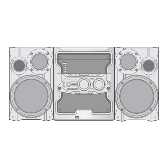
Page 48: Section 4. Speaker Section
SECTION 4. SPEAKER SECTION ❏ MODEL: LMS-W550 - 4-1 -... - Page 49 - 4-2 -...