Sony CDX-GT57UP Service Manual
Hide thumbs
Also See for CDX-GT57UP:
- Operating instructions manual (64 pages) ,
- Owner's record (35 pages)
Table of Contents
Advertisement
Quick Links
SERVICE MANUAL
Ver. 1.0 2012.06
• The tuner and CD sections have no adjustments.
FOR UNITED STATES CUSTOMERS. NOT
APPLICABLE IN CANADA, INCLUDING
IN THE PROVINCE OF QUEBEC.
POUR LES CONSOMMATEURS AUX
ÉTATS-UNIS. NON APPLICABLE AU
CANADA, Y COMPRIS LA PROVINCE DE
QUÉBEC.
AUDIO POWER SPECIFICATIONS
CEA2006 Standard
Power Output: 17 Watts RMS 4 at
4 Ohms < 1% THD+N
SN Ratio: 80 dBA
(reference: 1 Watt into 4 Ohms)
Tuner section
FM
Tuning range: 87.5 – 107.9 MHz
Antenna (aerial) terminal:
External antenna (aerial) connector
Intermediate frequency: 25 kHz
Usable sensitivity: 8 dBf
Selectivity: 75 dB at 400 kHz
Signal-to-noise ratio: 80 dB (stereo)
Separation: 50 dB at 1 kHz
Frequency response: 20 – 15,000 Hz
9-893-495-01
Sony Corporation
2012F33-1
©
2012.06
Published by Sony Techno Create Corporation
CDX-GT57UP
Model Name Using Similar Mechanism
Mechanism Type
Optical Pick-up Name
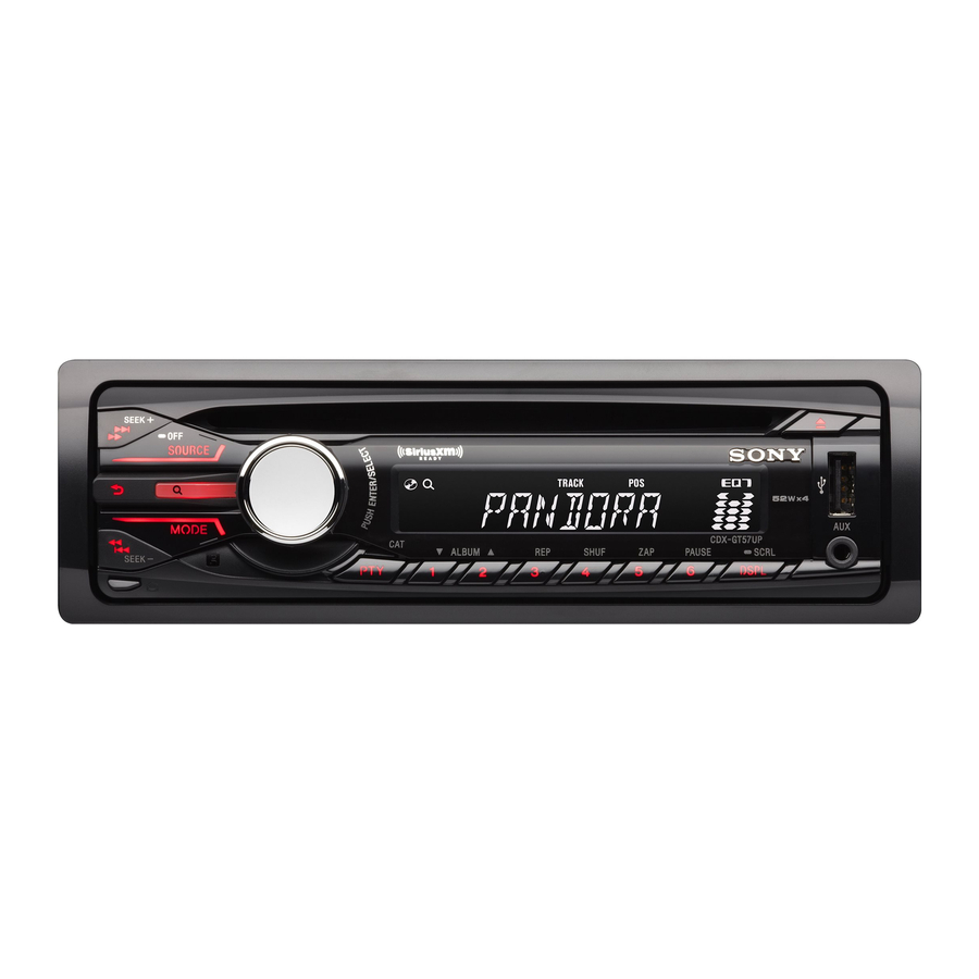
SPECIFICATIONS
AM
Tuning range: 530 – 1,710 kHz
Antenna (aerial) terminal:
External antenna (aerial) connector
Intermediate frequency:
9,115 kHz or 9,125 kHz/5 kHz
Sensitivity: 26 μV
CD Player section
Signal-to-noise ratio: 120 dB
Frequency response: 10 – 20,000 Hz
Wow and flutter: Below measurable limit
USB Player section
Interface: USB (Full-speed)
Maximum current: 1 A
Power amplifier section
Output: Speaker outputs
Speaker impedance: 4 – 8 ohms
Maximum power output: 52 W × 4 (at 4 ohms)
FM/AM COMPACT DISC PLAYER
US Model
Canadian Model
CDX-GT56UI
MG-101CA-188
DAX-25A
General
Outputs:
Audio outputs terminal (rear/sub switchable)
Power antenna (aerial)/Power amplifier control
terminal (REM OUT)
Inputs:
SiriusXM input terminal
Remote controller input terminal
Antenna (aerial) input terminal
AUX input jack (stereo mini jack)
USB port
Power requirements: 12 V DC car battery
(negative ground (earth))
Dimensions: Approx. 178 × 50 × 179 mm
1
× 2 × 7
1
(7
/
/
in) (w/h/d)
8
8
Mounting dimensions: Approx. 182 × 53 × 162 mm
1
× 2
1
× 6
1
(7
/
/
/
in) (w/h/d)
4
8
2
Mass: Approx. 1.2 kg (2 lb 11 oz)
Supplied accessories:
Remote commander: RM-X211
Parts for installation and connections (1 set)
Design and specifications are subject to change
without notice.
Advertisement
Table of Contents

Related Manuals for Sony CDX-GT57UP


Summary of Contents for Sony CDX-GT57UP
- Page 1 Usable sensitivity: 8 dBf Selectivity: 75 dB at 400 kHz Signal-to-noise ratio: 80 dB (stereo) Separation: 50 dB at 1 kHz Frequency response: 20 – 15,000 Hz FM/AM COMPACT DISC PLAYER 9-893-495-01 Sony Corporation 2012F33-1 © 2012.06 Published by Sony Techno Create Corporation...
- Page 2 Do not touch the soldering iron on the same conductor of the TIONNEMENT. NE REMPLACER CES COMPOSANTS QUE circuit board (within 3 times). PAR DES PIÈCES SONY DONT LES NUMÉROS SONT DON- • Be careful not to apply force on the conductor when soldering NÉS DANS CE MANUEL OU DANS LES SUPPLÉMENTS...
-
Page 3: Table Of Contents
CDX-GT57UP SECTION 1 SERVICING NOTES TABLE OF CONTENTS NOTES ON HANDLING THE OPTICAL PICK-UP BLOCK OR BASE UNIT SERVICING NOTES ..........The laser diode in the optical pick-up block may suffer electro- GENERAL static break-down because of the potential difference generated by .............. - Page 4 CDX-GT57UP EXTENSION CABLE AND SERVICE POSITION When repairing or servicing this set, connect the jig cable (exten- sion cable (CD mecha)) as shown below. • Connect the MAIN board (CN700) and the SERVO board (CN401) with the jig cable. Jig cable: Part No.
-
Page 5: General
CDX-GT57UP SECTION 2 This section is extracted GENERAL from instruction manual. Equipment used in illustrations (not supplied) Appareils utilisés dans les illustrations (non fournis) Front speaker Subwoofer Power amplifier Rear speaker Haut-parleur avant Caisson de graves Amplificateur de puissance Haut-parleur arrière... - Page 6 Precautions Unité: mm (po) You may not be able to install this unit in some makes of Japanese cars. In such a case, consult your Sony dealer. Choose the installation location carefully so that the unit 182 (7 will not interfere with normal driving operations.
-
Page 7: Disassembly
CDX-GT57UP SECTION 3 DISASSEMBLY • This set can be disassembled in the order shown below. 3-1. DISASSEMBLY FLOW FRONT PANEL SECTION Note: Illustration of disassembly is omitted. 3-2. COVER (Page 7) 3-3. SUB PANEL BLOCK (Page 8) 3-4. CD MECHANISM DECK (MG-101CA-188) (Page 8) 3-5. -
Page 8: Sub Panel Block
CDX-GT57UP 3-3. SUB PANEL BLOCK 2 two claws 2 two claws 1 two screws (PTT2.6 3 sub panel block 3-4. CD MECHANISM DECK (MG-101CA-188) 5 bracket (CD) 6 CD mechanism deck 4 two screws (MG-101CA-188) (PTT2.6 1 screw (PTT2.6 2 Lift up the CD mechanism deck block. -
Page 9: Main Board
CDX-GT57UP 3-5. MAIN BOARD 3 screw (PTT2.6 1 fuse (blade type) (auto fuse) (10A/32V) (FU601) 2 three ground point screws (PTT2.6 3 screw (PTT2.6 4 MAIN board 3-6. SERVO BOARD 2 toothed lock screw (M1.7 2.5) 2 toothed lock screw (M1.7... -
Page 10: Chassis (T) Sub Assy
CDX-GT57UP 3-7. CHASSIS (T) SUB ASSY 1 two screws (M1.7 2.5) 1 two screws (M1.7 2.5) 3 chassis (T) sub assy 2 claw 3-8. ROLLER ARM ASSY 5 roller arm assy 4 gear (HRA) 1 spring (RAL) 3 washer 2 spring (RAR) -
Page 11: Chassis (Op) Assy
CDX-GT57UP 3-9. CHASSIS (OP) ASSY 8 chassis (OP) assy 1 tension spring (KF) 6 two coil springs (damper) (natural) 7 coil spring (damper) (blue) 4 slider (R) 3 lever (D) 2 gear (LE1) 3-10. CHUCKING ARM SUB ASSY 3 chucking arm sub assy 1 spring Note 1: Have this portion receive the chassis. -
Page 12: Sled Motor Assy
CDX-GT57UP 3-11. SLED MOTOR ASSY 2 three serration screws 3 sled motor assy 1 spring turn table spring stand Note 2: Never remove these parts since they were adjusted. bearing (F) – – stand Note 1: Place the stand with care not to touch the turn table. -
Page 13: Optical Pick-Up Section
CDX-GT57UP 3-12. OPTICAL PICK-UP SECTION 2 optical pick-up section Note: Be careful not to touch the lens and hologram terminal when removing the optical pick-up section. – bottom side view – 3-13. OPTICAL PICK-UP 1 tapping screw (P 1.4) 2 leaf spring (OPS) -
Page 14: Diagrams
CDX-GT57UP SECTION 4 DIAGRAMS 4-1. BLOCK DIAGRAM - AUDIO INPUT Section - CD MECHANISM DECK BLOCK (MG-101CA-188) FL, RL, SUB (Page 15) FPI1 DAO3 (F_L-CH) FPI2 DAO2 (F_R-CH) R-CH FNI1 FNI2 DAO4 (R_L-CH) DAO1 (R_R-CH) R-CH CD HEAD AMP, DAO5 (SUB-CH) -
Page 15: Block Diagram - Audio Output Section
CDX-GT57UP 4-2. BLOCK DIAGRAM - AUDIO OUTPUT Section - ELECTRICAL VOLUME, INPUT SELECTOR IC401 FL, RL, SUB (Page 14) 33 AU_IN_FL AU_OUT_FL 36 31 AU_IN_RL J402 AU_OUT_SL 40 REAR/SUB AUDIO OUT R-CH 30 AU_IN_SUB J901 AU_OUT_RL R-CH AUX_LCH AU_OUT_L PRE_L... -
Page 16: Block Diagram - Panel, Power Supply Section
CDX-GT57UP 4-3. BLOCK DIAGRAM - PANEL, POWER SUPPLY Section - SYSTEM CONTROLLER IC501 (3/3) (Page 14) RESET XOUT RESET X502 +3.3V SIGNAL 32.768kHz RESET 12 REGULATOR GENERATOR IC402 IC403 CN301 (2/2) OSCOUT LIQUID CRYSTAL X501 BU +3.3V REGULATOR DISPLAY PANEL LCD CONTROL 7.92MHz... - Page 17 CDX-GT57UP THIS NOTE IS COMMON FOR PRINTED WIRING BOARDS AND SCHEMATIC DIAGRAMS. • Waveforms (In addition to this, the necessary note is printed in each block.) – MAIN Board – For Printed Wiring Boards. For Schematic Diagrams. IC501 qa (XOUT)
-
Page 18: Printed Wiring Board - Main Section (1/2)
CDX-GT57UP 4-4. PRINTED WIRING BOARD - MAIN Section (1/2) - • : Uses unleaded solder. X501, X701 MAIN BOARD (COMPONENT SIDE) R308 C457 C878 C877 C876 C319 Q401 Q403 Q405 Q404 Q406 Q402 R303 R873 R403 C317 R304 R875 R874... -
Page 19: Printed Wiring Boards - Main Section (2/2)
CDX-GT57UP 4-5. PRINTED WIRING BOARDS - MAIN Section (2/2) - • : Uses unleaded solder. (FRONT VIEW) J402 REAR/SUB AUDIO OUT J801 FU601 MAIN BOARD CN802 REMOTE IN SIRIUSXM IN (CONDUCTOR SIDE) W002 (ANTENNA IN) WHT/BLK FRONT LCH (–) FB803... -
Page 20: Schematic Diagram - Main Section (1/4)
CDX-GT57UP 4-6. SCHEMATIC DIAGRAM - MAIN Section (1/4) - • See page 26 for IC Block Diagrams. MAIN BOARD (1/4) IC B/D IC301 POWER AMP, REGULATOR IC301 TDF8556AJ/N5 CN301 FRONT LCH (-) FRONT LCH (+) REAR LCH (-) REAR LCH (+) -
Page 21: Schematic Diagram - Main Section (2/4)
CDX-GT57UP 4-7. SCHEMATIC DIAGRAM - MAIN Section (2/4) - • See page 17 for Waveforms. • See page 26 for IC Block Diagrams. • See page 28 for IC Pin Function Description. MAIN BOARD (2/4) MAIN A_ATT BOARD (1/4) (Page 20) -
Page 22: Schematic Diagram - Main Section (3/4)
CDX-GT57UP 4-8. SCHEMATIC DIAGRAM - MAIN Section (3/4) - • See page 17 for Waveforms. • See page 28 for IC Pin Function Description. MAIN BOARD (3/4) JL728 C771 R742 C787 C776 JL730 C717 C782 C779 C789 0.01 2200p FB782... -
Page 23: Schematic Diagram - Main Section (4/4)
CDX-GT57UP 4-9. SCHEMATIC DIAGRAM - MAIN Section (4/4) - • See page 17 for Waveforms. • See page 26 for IC Block Diagrams. • See page 28 for IC Pin Function Description. MAIN BOARD (4/4) R674 R673 C616 R667 C613... -
Page 24: Printed Wiring Board - Key Board
CDX-GT57UP 4-10. PRINTED WIRING BOARD - KEY Board - • : Uses unleaded solder. KEY BOARD (COMPONENT SIDE) LED932, 934, 936, 938, 940, 942, LED946,S901 LED944, 946, 950, 952, 954 LED950, S902 S901 SOURCE LED901 (LCD BACK LIGHT) LED936, S903... -
Page 25: Schematic Diagram - Key Board
CDX-GT57UP 4-11. SCHEMATIC DIAGRAM - KEY Board - • See page 26 for IC Block Diagrams. KEY BOARD R998 R901 FB902 IC902 PNJ4813M01S0 FB901 J901 R902 R903 LED934 LSW905 SML-D12V8WT86TN SCRL LED901 S[4] S[21] DSPL R905 NESW505DT-A0-UV SEG4 SEG21 S901... - Page 26 CDX-GT57UP • IC Block Diagrams IC681, 682 NJM2878F3-15 (TE2) – MAIN Board – IC301 TDF8556AJ/N5 I2C_SIO THERMAL OUT-FL– C BUS PROTECTION BANDGAP I2C_SCK REFERENCE OUT-FL+ OUT-RL– P-GND1 OUT-RL+ IN-RL IN-FL S-GND PROTECTION/ DIAGNOSTIC IN-FR IN-RR BEEP OUT-RR+ P-GND3 OUT-RR– OUT-FR+...
- Page 27 CDX-GT57UP IC1300 OZ539IGN-A1-0-TR BST 1 VREF OSCILLATOR LX 2 REFERENCE GENERATOR OVER CURRENT PROTECTION GNDA VIN 3 EN_SYS 4 USBOUT 5 FB_USB 6 SS_SYS ADJUSTMENT GENERATOR CHARGE EN_USB PUMP VIC_USB USBIN OVER-CURRENT ISET_USB LIMIT VOUT_SYS (USBIN) UVLS FAULT PROTECTION –...
- Page 28 CDX-GT57UP • IC Pin Function Description MAIN BOARD IC501 R5F3650KBDZ74FA (SYSTEM CONTROLLER) Pin No. Pin Name Description LCD_SO Serial data output to the liquid crystal display driver LCD_CLK Serial clock signal output to the liquid crystal display driver NOSE_SW Front panel remove/attach detection signal input terminal “L”: Front panel is attached...
- Page 29 CDX-GT57UP Pin No. Pin Name Description DIAG Diagnostic signal input from the power amplifi er AMPSTB Standby control signal output to the power amplifi er Not used VCC2 Power supply terminal (+3.3V) F_AUX_ATT Muting on/off control signal output terminal Not used...
- Page 30 CDX-GT57UP MAIN BOARD IC601 M321FEFG-7KN3 (SY (CD DRIVE/USB CONTROLLER) Pin No. Pin Name Description AVSS Ground terminal VREFH Reference voltage (+3.3V) input terminal (for A/D converter) RESET Reset signal input from the system controller “L”: reset MODE Operation mode setting terminal Fixed at “L”...
- Page 31 CDX-GT57UP Pin No. Pin Name Description TRACEDATA0 to 64 to 67 Not used TRACEDATA3 CP_SDA Serial data input/output for the EEPROM CP_SCL Serial data transfer clock signal output to the EEPROM Not used CP_RESET Reset signal output to the EEPROM...
- Page 32 CDX-GT57UP MAIN BOARD IC701 TC94A99FG-003 (SY, H (CD HEAD AMP, DIGITAL SERVO PROCESSOR, AUDIO DSP) Pin No. Pin Name Description LPFO Signal output from the operation amplifi er for PLL loop fi lter PVREF Reference voltage (+1.65V) input terminal VCOF Terminal for VCO fi...
- Page 33 CDX-GT57UP Pin No. Pin Name Description ADVDD3 Power supply terminal (+3.1V) ADIN1 (IN_L-CH) Audio signal input terminal (L channel) ADVREFL Reference voltage output terminal ADVCM Reference voltage output terminal ADVREFH Reference voltage output terminal ADIN2 (IN_R-CH) Audio signal input terminal (R channel)
-
Page 34: Exploded Views
CDX-GT57UP SECTION 5 EXPLODED VIEWS Note: • -XX and -X mean standardized parts, so • The mechanical parts with no reference The components identifi ed by mark 0 they may have some difference from the number in the exploded views are not sup- or dotted line with mark 0 are critical for original one. -
Page 35: Front Panel Section
CDX-GT57UP 5-2. FRONT PANEL SECTION not supplied (for FRONT PANEL) not supplied (KEY board) RE901 not supplied IC902 CCB1 LCD901 J901 CN902 not supplied Note: Refer to the servicing notes “NOTE FOR REPLACEMENT OF THE USB CONNECTOR (CN902) AND THE AUX JACK (J901)”... -
Page 36: Cd Mechanism Deck Section (Mg-101Ca-188)
CDX-GT57UP 5-3. CD MECHANISM DECK SECTION (MG-101CA-188) CDM1 DAX1 not supplied supplied not supplied not supplied not supplied not supplied not supplied SENSOR board not supplied not supplied not supplied not supplied not supplied Ref. No. Part No. Description Remark Ref. -
Page 37: Electrical Parts List
CDX-GT57UP SECTION 6 ELECTRICAL PARTS LIST Note: • Due to standardization, replacements in • CAPACITORS When indicating parts by reference num- the parts list may be different from the uF: μF ber, please include the board name. parts specifi ed in the diagrams or the com- •... - Page 38 CDX-GT57UP MAIN Ref. No. Part No. Description Remark Ref. No. Part No. Description Remark R942 1-216-864-11 SHORT CHIP C308 1-127-715-11 CERAMIC CHIP 0.22uF C309 1-100-354-21 ELECT CHIP 220uF 6.3V R944 1-216-820-11 METAL CHIP 1/10W C311 1-127-715-11 CERAMIC CHIP 0.22uF R946...
- Page 39 CDX-GT57UP MAIN Ref. No. Part No. Description Remark Ref. No. Part No. Description Remark C601 1-100-597-91 CERAMIC CHIP 0.1uF C756 1-164-937-11 CERAMIC CHIP 0.001uF C605 1-100-567-81 CERAMIC CHIP 0.01uF C759 1-100-567-81 CERAMIC CHIP 0.01uF C606 1-100-567-81 CERAMIC CHIP 0.01uF C760 1-100-597-91 CERAMIC CHIP 0.1uF...
- Page 40 CDX-GT57UP MAIN Ref. No. Part No. Description Remark Ref. No. Part No. Description Remark D401 6-502-961-01 DIODE DA2J10100L < JACK > D403 6-500-335-01 DIODE MC2838-T112-1 1-843-172-11 JACK (ANT) (ANTENNA IN) D530 6-502-131-01 DIODE LRB751V-40T1G J401 1-822-713-11 JACK, PIN 2P (REAR/SUB AUDIO OUT)
- Page 41 CDX-GT57UP MAIN Ref. No. Part No. Description Remark Ref. No. Part No. Description Remark R403 1-216-833-11 METAL CHIP 1/10W R555 1-218-990-81 SHORT CHIP R404 1-218-953-11 METAL CHIP 1/16W R556 1-218-957-11 METAL CHIP 2.2K 1/16W R405 1-216-833-11 METAL CHIP 1/10W R557...
- Page 42 CDX-GT57UP MAIN SENSOR Ref. No. Part No. Description Remark Ref. No. Part No. Description Remark R654 1-218-977-11 METAL CHIP 100K 1/16W R742 1-216-841-11 METAL CHIP 1/10W R655 1-216-097-11 METAL CHIP 100K 1/10W R743 1-218-967-11 METAL CHIP 1/16W R656 1-218-977-11 METAL CHIP...
- Page 43 CDX-GT57UP SERVO Ref. No. Part No. Description Remark Ref. No. Part No. Description Remark A-1866-089-A SERVO BOARD, COMPLETE PARTS FOR INSTALLATION AND CONNECTIONS ********************** ************************************** When the SERVO board is defective, exchange the complete mounted board. X-2548-178-1 FRAME ASSY, FITTING...
- Page 44 CDX-GT57UP REVISION HISTORY Checking the version allows you to jump to the revised page. Also, clicking the version at the top of the revised page allows you to jump to the next revised page. Ver. Date Description of Revision 2012.06...