Table of Contents
Advertisement
Quick Links
/
SERVICE MANUAL
MR816CSX
Steinberg and Cubase are the registered trademarks of Steinberg Media Technologies GmbH.
(Steinberg および Cubase は、Steinberg Media Technologies GmbH 社(以下「Steinberg」 )の登録商標です。 )
SPECIFICATIONS(総合仕様) ..............................................4/6
PANEL LAYOUT(パネルレイアウト) ......................................8
CIRCUIT BOARD LAYOUT(ユニットレイアウト) .................9
WIRING(束線組込図) ..............................................................9
DISASSEMBLY PROCEDURE(分解手順) ............................10
LSI PIN DESCRIPTION(LSI 端子機能表) .............................14
IC BLOCK DIAGRAM(IC ブロック図) ..................................21
CIRCUIT BOARDS(シート基板図) .......................................23
(ファームウェアバージョンの確認) ..................................34/35
BACKUP(バックアップ) ..................................................36/38
INITIAL SETTING(出荷時の設定) .........................................39
FACTORY SET(ファクトリーセット) ..................................40
TEST PROGRAM(テストプログラム) .............................41/53
BOOT SEQUENCE(起動シーケンス) . ............................. 65/66
SY
011926
HAMAMATSU, JAPAN
200809-オー プンプライス
'08.09
Advertisement
Table of Contents

Related Manuals for Yamaha Steinberg MR816SCX


Summary of Contents for Yamaha Steinberg MR816SCX
-
Page 1: Table Of Contents
SERVICE MANUAL MR816CSX Steinberg and Cubase are the registered trademarks of Steinberg Media Technologies GmbH. (Steinberg および Cubase は、Steinberg Media Technologies GmbH 社(以下「Steinberg」 )の登録商標です。 ) CONTENTS(目次) SPECIFICATIONS(総合仕様) ..........4/6 PANEL LAYOUT(パネルレイアウト) ........8 CIRCUIT BOARD LAYOUT(ユニットレイアウト) ....9 WIRING(束線組込図) ..............9 DISASSEMBLY PROCEDURE(分解手順) ......10 LSI PIN DESCRIPTION(LSI 端子機能表) ......14 IC BLOCK DIAGRAM(IC ブロック図)... - Page 2 IMPORTANT NOTICE This manual has been provided for the use of authorized Yamaha Retailers and their service personnel. It has been assumed that basic service procedures inherent to the industry, and more specifically Yamaha Products, are already known and understood by the users, and have therefore not been restated.
- Page 3 MR816CSX/MR816X SAVING DATA(データの保存) Saving and backing up your data • Storing the settings to internal memory of the MR816 CSX/MR816 X must be performed from the MR Editor on the computer. If you use the MR816 CSX/MR816 X with MR Editor, you can store the settings to internal memory by storing the settings as a Scene or recalling the Scene on the MR Editor.
-
Page 4: Contents(目次) Specifications(総合仕様
MR816CSX/MR816X SPECIFICATIONS Electrical Characteristics Internal 44.1 kHz, 48 kHz, 88.2 kHz, 96 kHz Sample Rate External 44.1kHz, 48kHz, 88.2kHz, 96kHz (± 0.1%) Total Harmonic Distortion GAIN: Minimum 0.004% or less (1 kHz @ +18 dB, into 600 Ω) fs = 48 kHz 20 Hz−20 kHz, +1, -3 dB @ +4 dB, into 600 Ω... - Page 5 MR816CSX/MR816X Functions Analog Input MIC Preamp Discrete Class-A MIC preamp (Inverted Darlington Circuitry) [+48 V] button +48 V DC (Phantom Power switch) [PAD] button 0/26 dB Gain knob 44 dB variable (-60 dB to -16 dB) Phase Normal/Reversed (controlled via a computer) Input Channels 1 −...
- Page 6 MR816CSX/MR816X 総合仕様 電気的特性 Internal 44.1kHz、48kHz、88.2kHz、96kHz サンプリング周波数 External 44.1kHz、48kHz、88.2kHz、96kHz( 各± 0.1%) 全高調波歪 GAIN:最小 0.004% 以下(1kHz @ +18dB、負荷:600 Ω) fs=48kHz 20Hz 〜 20kHz、+1、-3dB @ +4dB、負荷:600 Ω 周波数特性 (CH IN → LINE OUT) fs=96kHz 20Hz 〜 40kHz、+1、-3dB @ +4dB、負荷:600 Ω 104dB DA コンバータ(LINE OUT) ダイナミックレンジ (最大レベル出力時の S/N 比) 97dB AD+DA( → LINE OUT) -118dB 等価入力ノイズ -86dB 残留出力ノイズ、アウトプットフェーダー:最小 GAIN:最大 -86dB(90dB S/N) LINE OUT ハム&ノイズ アウトプットチャンネルフェーダー:ノミナル値 (20Hz 〜 20kHz) PAD:オフ 全インプットチャンネルフェーダー:最小値 Rs=150 Ω GAIN:-60dB -53dB(57dB S/N)LINE OUT アウトプットチャンネルフェーダー:ノミナル値 PAD:オフ...
- Page 7 MR816CSX/MR816X 機能 アナログ入力 MIC プリアンプ Discrete Class-A MIC プリアンプ( インバーテッドダーリントン回路) [+48V] ボタン +48V DC [PAD] ボタン 0/26dB 入力チャンネル ゲインノブ 44dB 可変(-60dB 〜 -16dB) CH1 〜 8 PHASE 正相 / 逆相、ソフトウェアコントロール ハイパスフィルター OFF/80Hz(-12dB/oct.) 、ソフトウェアコントロール [HI-Z] スイッチ ON/OFF(CH1) 、入力インピーダンス:500k Ω AD コンバータ 24bit リニア、高性能デュアルビットデルタ / シグマ変換 [SIG/PEAK] ランプ -3dB 以上(赤) 、-40dB 〜 -3dB(緑) (クリッピングポイントを 0dB とした場合) アナログ出力 出力チャンネル マルチファンクションエンコーダーノブでのコントロール ( 全 1 〜 8 チャンネル同時) レベルコントロール...
-
Page 8: Panel Layout(パネルレイアウト
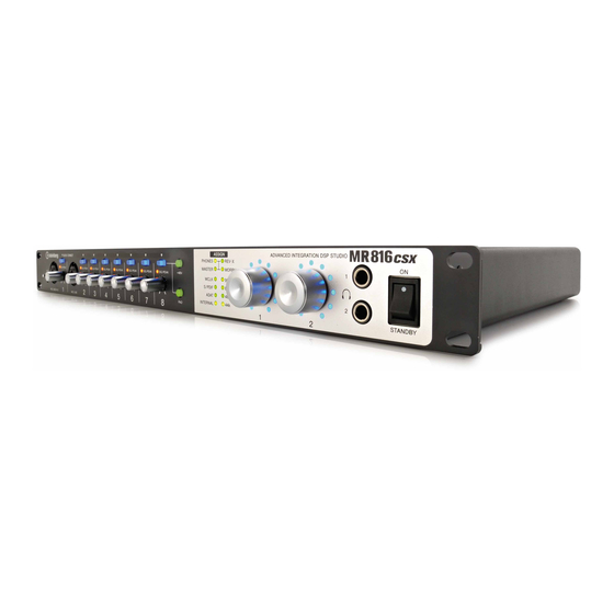
MR816CSX/MR816X PANEL LAYOUT(パネルレイアウト) • Front panel(フロントパネル) MR816CSX only (MR816CSX のみ) q [HI-Z] switch q [HI-Z] スイッチ w [MIC/LINE/HI-Z] jack 1 (analog input jack 1) and w [MIC/LINE/HI-Z] 端子 1 (アナログ入力端子 1) [MIC/LINE] jack 2 (analog input jack 2) [MIC/LINE] 端子 2 (アナログ入力端子 2) e [QUICK CONNECT] buttons (with LED lamps) e [QUICK CONNECT] ボタン(LED ランプ付き)... -
Page 9: Circuit Board Layout(ユニットレイアウト
MR816CSX/MR816X CIRCUIT BOARD LAYOUT(ユニットレイアウト) WIRING(束線組込図) CN301 (12P) CN151 AC wiring assembly CN101 (4P) (3P) CN104 CN601 CN651 CN701 (4P) (6P) (7P) (6P) CN102 CN851 (5P) CN901 (2P) (12P) CN850 (2P) CN103 (4P) CN800 (8P) CN111 (30P) CN602 CN652 CN702 (6P) (7P) (6P) CN112 (30P) -
Page 10: Disassembly Procedure(分解手順
MR816CSX/MR816X DISASSEMBLY PROCEDURE(分解手順) Precautions(注意事項) Notes on Flat Cable ※ フラットケーブルの注意 Contacts are visible from the back. Pay attention not to 接点が裏面から透けて見えます。コネクタにケーブルの 表・裏を逆に差込まないように注意して取り付けてくだ insert and install the cable to the connector inversely. さい。 (写真 1) (Photo 1) Front Side(表面) Back Side(裏面) Photo 1(写真... - Page 11 MR816CSX/MR816X Top Cover 1. トップカバー (所要時間:約 6 分) (Time required: About 6 minutes) Remove the following screws and slide the top cover 1-1 下記のネジを外して、トップカバーをリア側にス toward the rear side to remove it. (Fig. 1) ライドさせて外します。 (図 1) [142]: 16 pcs. [142]: 16 本...
- Page 12 MR816CSX/MR816X 3. AC シート、AC 束線 (所要時間:約 7 分) AC Circuit Board and Wiring Ass'y, AC 3-1 トップカバーを外します。 (1 項参照) (Time required: About 7 minutes) 3-2 [52A] のネジ 2 本と束線止めと共締めされている Remove the top cover. (See procedure 1.) [52B] のネジ 1 本、[56] のネジ 1 本を外して、AC Remove the two (2) screws marked [52A], the screw シートと...
- Page 13 MR816CSX/MR816X 5-4-2 Remove the wiring ass'y, PSW from the JK switch 5-4-2 JK スイッチアングルから PSW 束線を外します。 angle. (Fig. 5) (図 5) 5-4-3 Remove the two (2) angle brackets, U. The HP circuit 5-4-3 U 字金具 2 個を外して、HP シートを外します。 board can then be removed. (Fig. 5) ...
-
Page 14: Lsi Pin Description(Lsi 端子機能表
MR816CSX/MR816X LSI PIN DESCRIPTION(LSI 端子機能表) 1394AV-L (X6893A00) DICE II ..................... 16 ― AK4358VQ (X4289A00) DAC (Digital to Analog Converter) ..............20 AK5385BVF-E2 (X5364B00) ADC (Analog to Digital Converter) ............19 EP1C3T100C8N (X5691A00) FPGA....................14 MB87S1280 (X6363A00) SSP1 (MAIN/SUB) ..................18 MN101C027YB (XS71120R) CPU .......................15 S1L50553F21Y000 (X4195A0R) MCI (Gate Array) ................19 TSB41AB2PAP (XZ665A00) PHY .......................15 YAC523-VZ (X4325A00) EVR2 (Electric Variable Resistance 2) ............20... - Page 15 MR816CSX/MR816X MN101C027YB (XS71120R) CPU DM: IC150 NAME FUNCTION NAME FUNCTION Switch matrix data Switch matrix data MIDI transmit data VREF+ Power supply (+5V, analog) Switch matrix data Power supply (+5V) OSC2 Crystal oscillator (8MHz) OSC1 Crystal oscillator (8MHz) Ground Not used Not used MMOD Memory mode select (Grounded)
- Page 16 MR816CSX/MR816X 1394AV-L (X6893A00) DICE II DM: IC103 OUTER OUTER NAME FUNCTION NAME FUNCTION VSS3OP – I/O ground TEMO Test mode pin SRAM_WE SRAM write enable TCB[7] Test pin VDD3OP – I/O 3.3V GPIO4/SRAM_READY General purpose I/O / SRAM ready (read enable) I2C_CLK I2C Clock VDD1IH...
- Page 17 MR816CSX/MR816X OUTER OUTER NAME FUNCTION NAME FUNCTION VSS3OP – I/O ground AES_RX2 AES3 Receiver ch4/5 Address bus VDD3OP – I/O 3.3V DSAI_RX1 DSAI Receiver 1 data line VSS3OP – VSS3OP – I/O ground VSS3OP – DSAI_SYNCD DSAI Sync D I/O ground VSS3OP –...
- Page 18 MR816CSX/MR816X MB87S1280 (X6363A00) SSP1 (MAIN/SUB) DM: IC131, 132 NAME FUNCTION NAME FUNCTION WAITN Wait for external CPU MD[7] Data bus(ARM,DSP -> memory) IRQN_OUT Data bus(ARM,DSP -> memory) Output of interrupt information MD[6] VDDE VDDE +3.3V MD[5] SCANSW[4] MD[4] SCANSW[3] MD[3] Data bus(ARM,DSP ->...
- Page 19 MR816CSX/MR816X S1L50553F21Y000 (X4195A0R) MCI (Gate Array) DM: IC111 NAME FUNCTION NAME FUNCTION CLKI Power supply Clock CLKO RESET Reset Power supply Ground SCANENB Scan enable OUT4 Output ATPGENB OUT3 Ground INP2 PLLTEST Test INP1 Input PLLRES Reset INP0 PLLV Ground TESTENB Test enable Power supply...
- Page 20 MR816CSX/MR816X AK4358VQ (X4289A00) DAC (Digital to Analog Converter) DM: IC751 NAME FUNCTION NAME FUNCTION LOUT1- DAC1 Lch Negative Analog Output Pin DCLK DSD Clock Pin LOUT1+ DAC1 Lch Positive Analog Output Pin DSDL4 DAC4 DSD Lch Data Input Pin Zero Input Detect 3 Pin DAC4 DSD Rch Data Input Pin DZF3 DSDR4...
-
Page 21: Ic Block Diagram(Ic ブロック図
MR816CSX/MR816X IC BLOCK DIAGRAM(IC ブロック図) SN74HCU04NSR (XW842A0R) SN74AHC08PWR (X2713A00) SN74AHC14PWR (X3098A00) DM: IC108 DM: IC115, 116, 750 DM: IC138 Hex Inverter Quad 2 Input AND Hex Inverter SN75121NSR (XU816A00) SN74AHCT245PWR (X2709A00) SN75124NSR (XV930A00) DM: IC803 DM: IC107 DM: IC106 SN74LV245APWR (X3693A0R) Dual Line Driver Triple Line Receiver DM: IC200... - Page 22 MR816CSX/MR816X AK4382AVT (X0661A00) DM: IC809, 810 Digital to Analog Converter MCLK Pin No. Pin Name Function MCLK Master clock input MCLK DZFL BICK Audio serial data clock De-emphasis Clock SDTI Audio serial data input μP Control Divider BICK DZFR CCLK Interface LRCK L/R clock...
-
Page 23: Circuit Boards(シート基板図
MR816CSX/MR816X CIRCUIT BOARDS(シート基板図) AC Circuit Board (X9234C0) ............32 DM Circuit Board (X9232D0) ..........24/26/28/30 HP Circuit Board (X9234C0) ............23 JK Circuit Board (X9234C0) ............23 PN Circuit Board (X9404C0) ............32/33 Note: See parts list for details of circuit board component parts. 注 : シートの部品詳細はパーツリストをご参照ください。... - Page 24 MR816CSX/MR816X DM Circuit Board to HP-CN201 INSERT I/O MIC/LINE INPUT to DM-CN702 to DM-CN652 to DM-CN602 to AC-CN103 GAIN 1 GAIN 2 GAIN 3 GAIN 4 GAIN 5 GAIN 6 MIC/LINE/HI-Z MIC/LINE to DM-CN651 to DM-CN601 HI-Z 2NA-WK58180...
- Page 25 MR816CSX/MR816X Scale: 70/100 to JK-CN301 to AC-CN103 S/PDIF, OPTICAL OUTPUT WCLK IN/OUT IEEE1394 (S400) IEEE1394 (S400) to AC-CN151 not installed N.C. not installed to PN-CN102 to PN-CN101 GAIN 6 GAIN 7 GAIN 8 to DM-CN701 Component side(部品側) 2NA-WK58180...
- Page 26 MR816CSX/MR816X DM Circuit Board 2NA-WK58180...
- Page 27 MR816CSX/MR816X Scale: 70/100 Component side(部品側) 3 layer(3 層) 2NA-WK58180...
- Page 28 MR816CSX/MR816X DM Circuit Board 2NA-WK58180...
- Page 29 MR816CSX/MR816X Scale: 70/100 Component side(部品側) 6 layer(6 層) 2NA-WK58180...
- Page 30 MR816CSX/MR816X DM Circuit Board 2NA-WK58180...
- Page 31 MR816CSX/MR816X Scale: 70/100 Pattern side(パターン側) 2NA-WK58180...
- Page 32 MR816CSX/MR816X PN Circuit Board QUICK CONNECT to DM-CN111 +48V to DM-CN112 MR816CSX only Component side(部品側) AC Circuit Board to DM-CN104 to DM-CN850 N.C. to AC wiring assembly to PSW wiring assembly to DM-CN851 Component side(部品側) AC: 2NA-WM06850 PN: 2NA-WM46170...
- Page 33 MR816CSX/MR816X PN Circuit Board Pattern side(パターン側) 2NA-WM06850...
-
Page 34: Firmware Version Check
MR816CSX/MR816X FIRMWARE VERSION CHECK ① Turn on the power of the MR816CSX/MR816X while holding down the [ASSIGN 2] encoder. Keep the [ASSIGN 2] encoder held down. ② Firmware BOOT version will be indicated on the LED around the [ASSIGN 1] encoder. Firmware PROGRAM version will be indicated on the LED around the [ASSIGN 2] encoder. -
Page 35: ファームウェアバージョンの確認
MR816CSX/MR816X ファームウェアバージョンの確認 ① [ASSIGN 2] エンコーダを押しながら MR816CSX/MR816X の電源を入れます。[ASSIGN 2] エンコーダは押したままにし ておきます。 ② [ASSIGN 1] エンコーダの周りの LED で、ファームウェアの BOOT 部のバージョンが表示されます。 [ASSIGN 2] エンコーダの周りの LED で、ファームウェアの PROGRAM 部のバージョンが表示されます。 バージョン番号の見方に関しては、下の『バージョン表示』を参照してください。 ③バージョンを確認したら、[ASSIGN 2] エンコーダを離します。 MR816CSX のみ 電源 ASSIGN 1 ASSIGN 2 (図 1) • バージョン表示 例)バージョン 1.23 の場合 各バージョンは下図で示される各 LED で表示されます。 メジャーバージョン... -
Page 36: Backup(バックアップ
MR816CSX/MR816X BACKUP Preparations: Connect the IEEE1394 terminal of the 1-2 Click the file icon (to the left of the Scene Name text MR816CSX/MR816X to the computer with box) in the upper part of the MR Editor screen and click an IEEE1394 cable. the "... - Page 37 MR816CSX/MR816X 2. Restoring procedure 2-3 Open the ".mre" file stored in the computer with the 2-1 Start the MR Editor with the same procedure as in "1. Backup procedure" and the scene data will be stored "1. Backup procedure". (See procedure 1-1) back on the MR816CSX/MR816X automatically.
- Page 38 MR816CSX/MR816X バックアップ 準備: MR816CSX/MR816X の IEEE1394 端 子 と コ ン 1-2 MR Editor の画面の上部にあるファイルのアイコ ピューターを IEEE1394 ケーブルで接続しておき ン(シーン名称のテキストボックスの左側にある) ます。 をクリックし、プルダウンメニューの『Save』を クリックします。 1. バックアップ手順 このアイコンをクリック プルダウンメニュー 1-1 MR816CSX/MR816X の電源を入れて通常モード で立ち上げてから、コンピューターで MR Editor (X9658A0) を起動します。 ※ 次の場合は、MR Editor を起動したときエラー表 示になります。 ● MR816CSX/MR816X とコンピューターが正し く接続されていない。 ● 先に MR816CSX/MR816X が立ち上がっていな い状態で、MR Editor を起動した。...
-
Page 39: Initial Setting(出荷時の設定
MR816CSX/MR816X 2. 復帰手順 2-3 「 1. バ ッ ク ア ッ プ 手 順 」 で コ ン ピ ュ ー タ ー に 保 2-1 「 1. バックアップ手順」と同じ手順で MR Editor を 存 し た .mre フ ァ イ ル を 開 く と、 自 動 的 に 起動します。... -
Page 40: Factory Set(ファクトリーセット
MR816CSX/MR816X FACTORY SET(ファクトリーセット) The following contents can be initialized by executing the ファクトリーセットを実行することで、以下の内容を初 Factory set. 期化することが出来ます。 • Mixer setup information (Flash ROM around SSP1) ・ ミキサー設定情報 (SSP1 周辺 FLASH ROM) • Wordclock related setup information ・ ワードクロック関連設定情報(SSP1 周辺 EEPROM) (EEPROM around SSP1) *ファクトリーセットを実行する前に、必ずユーザー * Be sure to save user data before executing Factory set. -
Page 41: Test Program(テストプログラム
MR816CSX/MR816X TEST PROGRAM “No. 0: ANALOG test mode” will be selected just after 1. Preparations entering the test program mode. • IEEE1394 repeater hub 2 pcs. Wordclock source is INTERNAL 96 kHz. [ex.:1394-RP2GPH by Sanwa Supply] “Analog test mode” will always be selected when none of •... - Page 42 MR816CSX/MR816X ① AD/DA, Digital Input/Output connection diagram 5. Test item 5-1. No. 0 ANALOG test 5-1-1. Outline This test mode is for checking device around analog audio and signal cable connection. 5-1-2. Main devices to be tested • A/D Converter •...
- Page 43 MR816CSX/MR816X ④ S/PDIF ⇔ Analog connection diagram • Muting Circuit DICEII activates the MUTE signal cable when the [QUICK CONNECT 7] button is pressed. Check that related devices are muted. Press the [QUICK CONNECT 7] button again to cancel muting. SSP1 activates the DA MUTE signal cable when the [QUICK CONNECT 8] button is pressed.
- Page 44 MR816CSX/MR816X • Input signal Check that the level of each output when the Use 1 kHz sine wave for input signal unless otherwise frequency is 20 Hz and 40 kHz are within the range specifi ed. shown below compared with the level when the Input the following signals to the INPUT terminals. frequency is 1 kHz.
- Page 45 MR816CSX/MR816X Measure the output level at the Headphones [1, 2] <2-7> Crosstalk (OUTPUT 1 – 8) terminals. Set up as in description marked in procedure Check that the noise levels are as follows: <2-1> (P. 44). Unit: [dBu] Then, adjust input level so that output level is as in the description below: INPUT Headphones 1, 2 Unit:[dBu] -60 or less MIC/LINE INPUT 1 – 4 OUTPUT OUTPUT LEVEL * Use 22 Hz HPF and 30 kHz LPF. OUTPUT 1 –...
- Page 46 MR816CSX/MR816X <2-11> Headphones volume attenuation • Input/output terminals Unconnected Set up as in description marked in procedure [INSERT I/O 1, 2]: <2-1> (P. 44). Set up as follows. • Controller settings Unless otherwise specifi ed, set up as follows. Headphones 1, 2 volume: MIN • CH INPUT Unit: [dBu] GAIN volume (CH 1 – 8) : Headphones 1 [PAD] switch (CH 1 – 8) : INPUT [Hi-Z] switch (CH 1) : ...
- Page 47 MR816CSX/MR816X <2-2-2> Frequency characteristics *4: Check that level differences between channels are as follows: Set up as in description marked in procedure <2-2-1> (P. 46). Tolerance Check that the levels of each output when the 2 dB or less frequency is 20 Hz and 40 kHz are within the range shown below compared with the level when the <2-1-2> Frequency Characteristics frequency is 1 kHz. Set up as in description marked in procedure Tolerance <2-1-1> (P. 46). Within +1/-3 dB Check that the level of each output when the * Measure only the [S/PDIF IN, OUT] (COAXIAL) frequency is 20 Hz and 40 kHz are within the range terminal. shown below compared with the level when the frequency is 1 kHz. <2-2-3> Distortion Tolerance Set up as in description marked ...
- Page 48 MR816CSX/MR816X <2-2-6> Jitter measurement (WORD CLOCK INTERNAL) Measure the [S/PDIF OUT] (COAXIAL) terminal. Set WORD CLOCK to INTERNAL. Check that the jitter measurement value is as follows: WORD CLOCK Tolerance 44.1 kHz 48 kHz 5 nsec or 88.1 kHz below ASSIGN 1 ASSIGN 2 96 kHz 1. MEMORY 1. MEMORY (Test item selection) (Test result) <2-2-7> Jitter measurement (WORD CLOCK EXT) (Fig. 11) Measure the [S/PDIF OUT] (COAXIAL) terminal. Set up the WORD CLOCK and frequency of input 5-2-4. Test contents sources as follows: The result of the test is OK if test result of all the ROM/ Check of WORD CLOCK IN: ...
- Page 49 MR816CSX/MR816X 5-3-2. Main devices to be tested • Panel micro computer 5-3-4. Test contents • LED Communication with the panel micro computer is checked before conducting the LED lighting test. Colors of LEDs are as follows: If the test result of the communication with the panel micro computer is NG, the test will be aborted before MR816X MR816CSX...
- Page 50 MR816CSX/MR816X (7) All the LEDs of the MR816CSX/MR816X will fl ash micro computer is NG, the test will be aborted before automatically after the sequential lighting. proceeding to the SWITCH test. Check visually again and press the [ASSIGN 1] • Panel micro computer encoder in case of OK or the [ASSIGN 2] encoder in The test is conducted automatically.
- Page 51 MR816CSX/MR816X between the SSP1 and SSP1 SUB, connection checking of the audio signal cable between the SSP1 and DICEII, and connection checking of the signal cables between the DICEII and audio interfaces. Digital I/O Mode is set to ADAT x4 + S/PDIF(coaxial), clock source is set to INTERNAL and nominal FS is set to 96 kHz automatically on entering the test.
- Page 52 MR816CSX/MR816X 5-6-5. Test contents If 3 nodes in total (two 1394 hubs and one MR816CSX/ (1) Connection checking of the A-BUS between the MR816X connected to the connectors) are recognized, the SSP1 and connection checking of the audio signal test result is OK. cable between the SSP1 and DICEII are conducted The checking is conducted automatically and the test item automatically on entering the test.
- Page 53 MR816CSX/MR816X テストプログラム 1. 準備 テ ス ト プ ロ グ ラ ム モ ー ド に 入 っ た 直 後 は、 「No.0 : 治具 ANALOG 検査モード」となります。 ・ IEEE1394 リピーターハブ 2 台 ワードクロックソースは INTERNAL 96kHz。 (例:サンワサプライ製 1394-RP2GPH) 「MEMORY」 、 「LED」 、 「SWITCH」 、 「ENCODER」 、 ・ IEEE1394 ケーブル ...
- Page 54 MR816CSX/MR816X 5. テスト項目 ① AD/DA、Digital Input/Output 結線図 5-1. No.0 ANALOG 検査 5-1-1. 概要 ANALOG オーディオ周辺デバイスの検査や、信号線 の結線テストを行うための検査モードです。 5-1-2. 主な検査対象デバイス ・ A/D Converter ・ D/A Converter ・ Analog Volume Controller ・ Phantom +48 V ・ PAD ・ HI-Z ・ Muting Circuit 5-1-3. 検査方法 テ ス ト プ ロ グ ラ ム モ ー ド に 入 り「MEMORY」 、 「LED」 、 「SWITCH」 、 「ENCODER」 、 「DIGITAL I/ O」のどの検査項目も実行中では無い場合は、常に...
- Page 55 MR816CSX/MR816X ④ S/PDIF ⇔ Analog 結線図 再度、[+48 V] ボタンを押すと、Phantom +48 V 設定 モードが解除されます。 • Muting Circuit [QUICK CONNECT 7] ボタンを押すことで、DICEII が MUTE 信号線をアクティブにします。 これにより、関連デバイスが MUTE 状態になること を確認します。 再度 [QUICK CONNECT 7] ボタンを押すと、MUTE 状態が解除されます。 (図 7) [QUICK CONNECT 8] ボ タ ン を 押 す こ と で、SSP1 が DA MUTE 信号線をアクティブにします。また、 • Analog Volume Controller AK4382A、AK4358 に対し...
- Page 56 MR816CSX/MR816X • 入力信号 <2-3> 周波数特性 特に指定のない場合、入力信号は 1 kHz 正弦波とし <2-1> 項の , のついた条件に設定します。 ます。 各出力の 20 Hz、40 kHz でのレベルが 1 kHz の時 各入力端子への入力信号は以下のようにします。 と比べて以下の範囲内であることを確認します。 MIC/LINE INPUT 許容値 1 〜 8 +1/-3 dB 以内 System Balance Source 150 ohm Impedance <2-4> 歪率 <2-1> 項の , のついた条件に設定します。 • 測定器の設定 その後出力のレベルが以下の値になるように入力 指定のない場合、測定器の Filter 設定はしません。 レベルを調整します。 出力の歪率が下記の値であることを確認します。...
- Page 57 MR816CSX/MR816X Unit:[dBu] Signal Input Resistor (*3) CH (MIC) OUTPUT 1 〜 8 ヘッドフォン 1, 2 CH 1 Monitor 1‒R Noise Level -80 以下 -80 以下 CH 2 Monitor 1‒L * 22 Hz HPF、30 kHz LPF を使用します。 CH 3 Monitor 2‒R CH 4 Monitor 2‒L <2-7> クロストーク(OUTPUT 1 〜 8) *入力 CH 1 〜 4 の [PAD] スイッチを ON にします。 <2-1> 項 (P. 56) の のついた条件に設定します。...
- Page 58 MR816CSX/MR816X <2-11> ヘッドフォンボリューム減衰量 • 操作子設定 特に指定のない場合、以下のように設定します。 <2-1> 項 (P. 56) の の条件に設定します。 下記のように設定します。 • CH INPUT GAIN ボリューム (CH 1 〜 8): ヘッドフォン 1, 2 ボリューム : MIN [PAD] スイッチ (CH 1 〜 8): Unit: [dBu] [Hi-Z] スイッチ (CH 1): ヘッドフォン 1 [+48V] スイッチ (CH 1 〜 8) : INPUT ・Muting Circuit [QUICK CONNECT 7,8] -80 以下 ‒ Mute: ‒...
- Page 59 MR816CSX/MR816X <2-2-3> 歪率 <2-1-2> 周波数特性 <2-1-1> 項 (P. 58) の のついた条件に設定します。 <2-2-1> 項 (P. 58) の のついた条件に設定します。 その後、出力のレベルが以下の値になるように入 各出力の 20 Hz、40 kHz でのレベルが、1 kHz の 力レベルを調整します。 時と比べて以下の範囲内であることを確認します。 出力の歪率が下記の値になることを確認します。 許容値 Unit: [dBu] +1/-3 dB 以内 OUTPUT LEVEL Distortion 0.03 % 以下 <2-1-3> 歪率 * 22 Hz HPF、30kHz LPF を使用します。 <2-1-1> 項 (P. 58) の のついた条件に設定します。 * [S/PDIF IN, OUT](COAXIAL)端子のみ測定 その後、出力のレベルが以下の値になるように入 します。...
- Page 60 MR816CSX/MR816X <2-2-7> ジッター測定(WORD CLOCK EXT) 5-2-4. テスト内容 [S/PDIF OUT](COAXIAL)端子を測定します。 SSP1 周 辺 の 全 て の ROM/RAM の チ ェ ッ ク 結 果 が WORD CLOCK は以下を選択し、各入力ソースの OK となることで、 本テストの結果が OK となります。 周波数設定を下記の値に設定します。 どれか一つでも NG であった場合は、本テストの結 WORD CLOCK IN の検査 : WCLK 果は NG となります。 ADAT の検査 : ADAT S/PDIF の検査...
- Page 61 MR816CSX/MR816X • パネルマイコン LED の色の内訳は以下の通りです。 チェックは自動的に行われます。 MR816X MR816CSX SSP1 からパネルマイコンのバージョンを正常に読み QUICK CONNECT 1 〜 8 緑 青 出すことが出来れば OK となります。OK の場合は、 SIG/PEAK 1 〜 8 緑 赤 緑 赤 引き続き LED 点灯チェックに移ります。 +48V 緑 緑 緑 緑 • LED PHONES 緑 緑 (1) LED 点灯チェックに移ると、まず MR816CSX/ MASTER 緑...
- Page 62 MR816CSX/MR816X (8) LED 検査が終了し、テスト項目選択モードへ移 • パネルマイコン ります。 チェックは自動的に行われます。 SSP1 からパネルマイコンのバージョンを正常に読み MR816CSX のみ 出すことが出来れば OK となります。OK の場合は、 引き続きスイッチチェックに移ります。 • スイッチ (図 13)LED 順次点灯の順番 (1) スイッチチェックに移ると、パネル上の全スイッ チの付近にある LED が点灯します。チェックを 5-4. No.3 SWITCH 検査 終えたスイッチの付近の LED は消灯し、検査の 5-4-1. 概要 進捗をガイドします。 PN シート上のスイッチやパネルマイコンのデバイ (2) ス イ ッ チ チ ェ ッ ク の 順 番 に 従 っ て、 ス イ ッ チ スチェックと、スイッチ、パネルマイコン、SSP1 間...
- Page 63 MR816CSX/MR816X タルオーディオインターフェースとの信号線の結線 チェックを行います。 本 検 査 に 入 る と 自 動 的 に、Digital I/O Mode が ADAT x4 + S/PDIF(coaxial)、 ク ロ ッ ク ソ ー ス が INTERNAL、ノミナル FS が 96kHz となります。 5-6-2. 主な検査対象デバイス ・SSP1 と SSP1 SUB 間の A-BUS ・SSP1 と DICEII、FPGA 間のオーディオ信号線 ・[WCLK] 端子...
- Page 64 MR816CSX/MR816X (2) その後、[WCLK]、[S/PDIF]、[adat] 端子のルー チェックは自動で行われ、検査終了後、OK ならば プバック結線による Lock チェック、オーディオ テスト項目選択モードへ移ります。 チェックが自動的に行われます。 (3) 以上で、テストが終了します。 6. その他、検査機能 6-1. FPGA バージョン表示 テスト終了後、自動的にテスト項目選択モードへ 6-1-1. 概要 移ります。 なお、テストの途中で [ASSIGN 2] エンコーダを DM シート上の FPGA のプログラムバージョンを、 押せば、DIGITAL I/O 検査を中断することがで MR816CSX/MR816X のパネル上の LED で確認する きます。 ことができます。 5-7. No.6 1394̲CONNECT 検査 6-1-2. 主な検査対象デバイス 5-7-1. 概要 ・FPGA DM シ...
-
Page 65: Boot Sequence(起動シーケンス
MR816CSX/MR816X BOOT SEQUENCE Operation fl ow of normal start-up (Turning on the power without holding any switch) Indication on the product Function Behavior of main signal lines All the LEDs go out Voltage of 3.3 V is applied to the IC137 system reset (voltage IC137: +3.3D detector). - Page 66 MR816CSX/MR816X 起動シーケンス 通常起動(電源 ON 時に、何もスイッチを押さない状態で起動した場合)での動作フロー 本体表示 動作 主な信号線の挙動 全ての LED が消灯 システムリセット(電圧検出器)IC137 に 3.3V 電圧が印加さ IC137:+3.3D れます。検出後約 10us 遅延して出力されます。 フラッシュ ROM(IC133) のリセットが解除されます。 IC133:/RESET CPU(IC131) のリセットが解除されます。 IC131:ICN フラッシュ ROM(IC133) の 0 番地よりプログラムをフェッチ IC131:CS0N(/CS0)、MA * (MMA[ * ])、MD * (MMD[ * ])、RDN、WRN 開始。BOOT 部プログラム動作開始。...
-
Page 67: Parts List
PARTS LIST CONTENTS(目次) OVERALL ASSEMBLY (総組立) ............2 ELECTRICAL PARTS (電気部品) ............. 5-24 Notes : DESTINATION ABBREVIATIONS A : Australian model M : South African model B : British model O : Chinese model C : Canadian model Q : South-east Asia model D : German model T : Taiwan model E : European model... - Page 68 MR816CSX/MR816X OVERALL ASSEMBLY(総組立) 148 x2 82 x3 148 x2 24 x3 48 x8 52 x3 46 x3 Top (上) Bottom (下) MR816X MR816CSX...
- Page 69 MR816CSX/MR816X • Top view(上面から見た図) MR816 SER No. UA00. . . yyyymm 00000000 PART NO. DESCRIPTION 部 品 名 REMARKS REF NO. QTY RANK OVERALL ASSEMBLY 立 MR816CSX/MR816X 総 組 OVERALL ASSEMBLY 総 組 立 MR816CSX (WK36740) OVERALL ASSEMBLY 総 組 立...
- Page 70 MR816CSX/MR816X PART NO. DESCRIPTION 部 品 名 REMARKS REF NO. QTY RANK WK837300 TOP COVER ト ッ プ カ バ ー 印 刷 品 MR816X WF266600 BIND HEAD P-TIGHT SCREW 3.0X8 MFZN2B3 P タ イ ト + B I N D WE87780R BIND HEAD TAPPING SCREW-S 3.0X6 MFZN2B3 S...
- Page 71 MR816CSX/MR816X ELECTRICAL PARTS(電気部品) AC/HP/JP and DM PART NO. DESCRIPTION 部 品 名 REMARKS REF NO. QTY RANK ELECTRICAL PARTS 電 気 部 品 MR816CSX/MR816X WM069700 CIRCUIT BOARD A C シ ー ト (WM06850)(X9234C0) WK582100 CIRCUIT BOARD H P シ ー ト...
- Page 72 MR816CSX/MR816X PART NO. DESCRIPTION 部 品 名 REMARKS REF NO. QTY RANK C122 US625100 CERAMIC CAPACITOR-BJ(CHIP) 0.100 10V K RECT. チ ッ プ セ ラ( B J ) C123 US662100 CERAMIC CAP.-CH 100P 50V J RECT. チ ッ プ セ ラ( C H ) C124 US625100 CERAMIC CAPACITOR-BJ(CHIP) 0.100 10V K RECT.
- Page 73 MR816CSX/MR816X PART NO. DESCRIPTION 部 品 名 REMARKS REF NO. QTY RANK C302 WN110600 CAP CERAMIC CHIP 4.700 25V K KAKUTE チ ッ プ 積 層 セ ラ コ ン C303 US14510R CERAMIC CAPACITOR-F (CHIP) 0.1000 25V Z RECT. チ ッ プ セ ラ( F ) C304 US063100 CHIP MULTILAYER CERAMIC 1000P 50V K RECT.
- Page 74 MR816CSX/MR816X PART NO. DESCRIPTION 部 品 名 REMARKS REF NO. QTY RANK -639 WH190800 CERAMIC CAPACITOR-CH(CHIP) 1000P 50V J KAKUTE チ ッ プ セ ラ( C H ) C642 WC890800 ELECTROLYTIC CAP. 1000 6.3V RVO ケ ミ コ ン P U R E C643 WC890800 ELECTROLYTIC CAP.
- Page 75 MR816CSX/MR816X PART NO. DESCRIPTION 部 品 名 REMARKS REF NO. QTY RANK C1138 WK175700 MONOLITHIC CERAMIC CAP. 0.33 16V K KAKU TE チ ッ プ 積 層 セ ラ コ ン C1139 US035100 CHIP MULTILAYER CERAMIC 0.1000 16V K RECT. チ...
- Page 76 MR816CSX/MR816X PART NO. DESCRIPTION 部 品 名 REMARKS REF NO. QTY RANK C1395 UU268100 ELECTROLYTIC CAP 100.00 50.0V RX TP ケ ミ コ ン F W -1410 UU268100 ELECTROLYTIC CAP 100.00 50.0V RX TP ケ ミ コ ン F W C1503 US064100 CHIP MULTILAYER CERAMIC 0.0100 50V K RECT.
- Page 77 MR816CSX/MR816X PART NO. DESCRIPTION 部 品 名 REMARKS REF NO. QTY RANK C1633 WQ331600 CAP ELECTROLYTIC 220.00 25.0V TATE ケ ミ コ ン C1634 US064100 CHIP MULTILAYER CERAMIC 0.0100 50V K RECT. チ ッ プ セ ラ( B ) C1636 UF065330 ELECTROLYTIC CAP.(CHIP) 0.33 50V チ...
- Page 78 MR816CSX/MR816X PART NO. DESCRIPTION 部 品 名 REMARKS REF NO. QTY RANK EM150 V I 2 4 3 1 0 0 EMI FILTER DSS6NB32A271Q93A L C フ ィ ル タ ー EM152 VZ14490R CHIP INDUCTOR NFM21CC101U1H3D エ ミ フ ィ ル チ ッ プ EM153 VZ14490R CHIP INDUCTOR NFM21CC101U1H3D エ...
- Page 79 MR816CSX/MR816X PART NO. DESCRIPTION 部 品 名 REMARKS REF NO. QTY RANK IC808 X8398A00 IC TC7SET08FU(T5L,JF) I C AND IC809 X0661A00 IC AK4382AVT I C DAC IC810 X0661A00 IC AK4382AVT I C DAC IC811 X3505A00 IC NJM2068M-D(TE2) I C OP AMP IC812 X3505A00 IC NJM2068M-D(TE2)
- Page 80 MR816CSX/MR816X PART NO. DESCRIPTION 部 品 名 REMARKS REF NO. QTY RANK -111 RF35456R CARBON RES. (CHIP) 56.0 D 1608 チ ッ プ 抵 抗 R112 VK58240R METAL FILM RESISTOR (CHIP) 390K 1/10 D RECT. チ ッ プ 金 被 抵 抗 R114 RD357100 CARBON RESISTOR (CHIP) 10.0K 63M J RECT.
- Page 81 MR816CSX/MR816X PART NO. DESCRIPTION 部 品 名 REMARKS REF NO. QTY RANK R301 RD357100 CARBON RESISTOR (CHIP) 10.0K 63M J RECT. チ ッ プ 抵 抗 R302 RD35410R CARBON RESISTOR 10.0 63M J RECT. チ ッ プ 抵 抗 R303 RD357100 CARBON RESISTOR (CHIP) 10.0K 63M J RECT.
- Page 82 MR816CSX/MR816X PART NO. DESCRIPTION 部 品 名 REMARKS REF NO. QTY RANK R586 RD15468R CARBON RESISTOR 68.0 1/4 J TP チ ッ プ 抵 抗 R587 RD15468R CARBON RESISTOR 68.0 1/4 J TP チ ッ プ 抵 抗 R588 RD15468R CARBON RESISTOR 68.0 1/4 J TP チ...
- Page 83 MR816CSX/MR816X PART NO. DESCRIPTION 部 品 名 REMARKS REF NO. QTY RANK R694 RD356330 CARBON RESISTOR (CHIP) 3.3K 63M J RECT. チ ッ プ 抵 抗 R695 RF35747R CARBON RESISTOR 47.0K D 1608 チ ッ プ 抵 抗 -698 RF35747R CARBON RESISTOR 47.0K D 1608 チ...
- Page 84 MR816CSX/MR816X PART NO. DESCRIPTION 部 品 名 REMARKS REF NO. QTY RANK -796 RD354750 CARBON RESISTOR 75.0 63M J RECT. チ ッ プ 抵 抗 R797 RF35747R CARBON RESISTOR 47.0K D 1608 チ ッ プ 抵 抗 -804 RF35747R CARBON RESISTOR 47.0K D 1608 チ...
- Page 85 MR816CSX/MR816X PART NO. DESCRIPTION 部 品 名 REMARKS REF NO. QTY RANK -1048 RD355100 CARBON RESISTOR (CHIP) 100.0 63M J RECT. チ ッ プ 抵 抗 R1049 RD358100 CARBON RESISTOR (CHIP) 100.0K 63M J RECT. チ ッ プ 抵 抗 -1052 RD358100 CARBON RESISTOR (CHIP) 100.0K 63M J RECT.
- Page 86 MR816CSX/MR816X PART NO. DESCRIPTION 部 品 名 REMARKS REF NO. QTY RANK R1378 RF35711R CARBON RESISTOR (CHIP) 11.0K D 1608 チ ッ プ 抵 抗 R1379 RF357100 CHIP CARBON FILM RES. 10.0K D 1608 チ ッ プ 抵 抗 R1380 RF357100 CHIP CARBON FILM RES. 10.0K D 1608 チ...
- Page 87 MR816CSX/MR816X PART NO. DESCRIPTION 部 品 名 REMARKS REF NO. QTY RANK R1606 RF458100 CHIP CARBON FILM RES. 100.0K D RECT. チ ッ プ 抵 抗 R1607 RF457100 CHIP CARBON FILM RES. 10.0K D RECT. チ ッ プ 抵 抗 R1608 RD356100 CARBON RESISTOR (CHIP) 1.0K 63M J RECT.
- Page 88 MR816CSX/MR816X DM and PN PART NO. DESCRIPTION 部 品 名 REMARKS REF NO. QTY RANK TR608 VV540200 TRANSISTOR 2SB1260 P,Q,R ト ラ ン ジ ス タ 2 S B TR609 V742170R TRANSISTOR 2SC3324-GR,BL チ ッ プ ト ラ ン ジ ス タ -613 V742170R TRANSISTOR 2SC3324-GR,BL...
- Page 89 MR816CSX/MR816X PART NO. DESCRIPTION 部 品 名 REMARKS REF NO. QTY RANK D044 WG139300 DIODE KDS4148U-RTK/P TE ダ イ オ ー ド D101 WG139300 DIODE KDS4148U-RTK/P TE ダ イ オ ー ド D201 WG139300 DIODE KDS4148U-RTK/P TE ダ イ オ ー...
- Page 90 MR816CSX/MR816X PART NO. DESCRIPTION 部 品 名 REMARKS REF NO. QTY RANK LD110 WJ833500 LED GREEN SML-512MW T86 チ ッ プ L E D MR816X VOL 10(Encoder1) LD111 WK151100 CHIP LED BLUE SMLE12BC7T チ ッ プ L E D MR816CSX VOL 11(Encoder1) LD111 WJ833500 LED GREEN SML-512MW T86 チ...
-
Page 91: Block Diagram(ブロックダイアグラム
CIRCUIT DIAGRAM CONTENTS(目次) BLOCK DIAGRAM(ブロックダイアグラム) ......3 CIRCUIT DIAGRAM(回路図) DM (001‒013) ..............4–16 PN ..................17 AC, HP, JK ................18 Notation for Circuit Diagrams (回路図表記上の注意) 1. How to identify inter-circuit board connectors (シート間コネクタの読み方について) This indicates the location of the counter inter-circuit board connector. (The alphabet indicates horizontal direction and the number indicates vertical direction.) Signal name... - Page 92 BLOCK DIAGRAM (MR816CSX/MR816X) MR816CSX/MR816X 2 IC123: 1,2,36,38,97-100 IC132: 95,100,101,103,125-128,132-137,139-141,143,152,153,155 Address,Data Bus 1 IC101: 22,25,26,30,31,42,51,52,56,61,62 +3.3D 3 IC131: 11,27,34,73,79,86,123,131,138,177,183,190 IC113: 1-8,16-25,26,48 +48A ON/OFF (1:8) /RESET FLASH +48A ON/OFF(1) 4 IC131: 4,12,20,21,29,30,33,43,61,83,97,104,114,129,147,165,172-174,196,201 IC112: 1,7,13,25,38,44 37,47 A[0:18],CS[0] +48A PAD ON/OFF (1:8) (8Mbit) /RD,/WR Hi-Z ON/OFF 11,28 A[0:18],CS[0,1,5]...
- Page 93 DM CIRCUIT DIAGRAM 001 (MR816CSX/MR816X) MR816CSX/MR816X GUID LABEL IEEE1394 (S400) IEEE1394 (S400) DICE2 EEPROM 32K : Not installed (未実装) : Ceramic Capacitor (セラミックコンデンサー) : Chip Resistor (チップ抵抗) DM CIRCUIT DIAGRAM 001 (MR816CSX/MR816X) 28CC1-2001035323-1 1...
- Page 94 DM CIRCUIT DIAGRAM 002 (MR816CSX/MR816X) MR816CSX/MR816X R1114N181A-TR (X7764A00) DAN217 (VV556300) S/PDIF IN, REGULATOR +1.8V DIODE ARRAY 0.3AX2 DM: IC110 DM: DA150, DA151 OPTICAL IN 1: V 1: ANODE 1 2: GND 2: CATHODE 2 3: CE or CE 3: CATHODE 1, 4: NC ANODE 2 5: V...
- Page 95 DM CIRCUIT DIAGRAM 003 (MR816CSX/MR816X) MR816CSX/MR816X SDRAM 16M FLASH ROM 8M REGULATOR DICE2 DICE2 R1172S181B (X7887A00) REGULATOR +1.8V DM: IC201 1: V 2: GND 3: CE or CE 4: NC 5: GND 6: V (GATE ARRAY) RB160M-30 (WC549600) DIODE DM: D201 1: ANODE 2: CATHODE : Not installed (未実装)...
- Page 96 DM CIRCUIT DIAGRAM 004 (MR816CSX/MR816X) MR816CSX/MR816X DICE2 TRANSCEIVER : Ceramic Capacitor (セラミックコンデンサー) DM CIRCUIT DIAGRAM 004 (MR816CSX/MR816X) 28CC1-2001035323-4 1...
- Page 97 DM CIRCUIT DIAGRAM 005 (MR816CSX/MR816X) MR816CSX/MR816X REGULATOR +1.5V N.C. FPGA CONFIG (FLASH) R1172S151D (X7565A00) REGULATOR +1.5V DM: IC125 1: V 2: GND 3: CE or CE 4: NC 5: GND 6: V RB160M-30 (WC549600) DIODE DM: D125 1: ANODE 2: CATHODE : Not installed (未実装)...
- Page 98 DM CIRCUIT DIAGRAM 006 (MR816CSX/MR816X) MR816CSX/MR816X INVERTER INVERTER REGULATOR +1.8V EEPROM 2K VOLTAGE DETECTOR to AC-CN151 <Page 18: G-4> SDRAM 64M SSP1 (MAIN) SSP1 (SUB) R1172S181B (X7887A00) RB160M-30 (WC549600) REGULATOR +1.8V DIODE DM: IC140 DM: D140 1: V 2: GND 3: CE or CE 4: NC 1: ANODE...
- Page 99 DM CIRCUIT DIAGRAM 007 (MR816CSX/MR816X) MR816CSX/MR816X Transistor Array to PN-CN101 <Page 17: A-2> LED current limiting resistor(LED電流制限抵抗) Part No. WK581800 WM775600 MODEL MR816X MR816CSX AND GATE R570 Not installed Installed R585 Not installed Installed AND GATE R588 Not installed Installed R591 Not installed Installed...
- Page 100 DM CIRCUIT DIAGRAM 008 (MR816CSX/MR816X) MR816CSX/MR816X D1F60 (VS20110R) DIODE DM: D601–604 OP AMP MIC/LINE/Hi-Z 1: ANODE OP AMP 2: CATHODE MA2J1110GL (VR496500) DIODE DM: D605–611 OP AMP INSERT I/O 1 1: ANODE 2: CATHODE INSERT I/O 2 RB160M-30 (WC549600) DIODE DM: D612 OP AMP REGULATOR +12V...
- Page 101 DM CIRCUIT DIAGRAM 009 (MR816CSX/MR816X) MR816CSX/MR816X D1F60 (VS20110R) DIODE DM: D901–904 1: ANODE 2: CATHODE MA2J1110GL (VR496500) DIODE OP AMP DM: D905–908 MIC/LINE INPUT 5 OP AMP 1: ANODE 2: CATHODE RB160M-30 (WC549600) OP AMP DIODE DM: D909 MIC/LINE INPUT 6 OP AMP REGULATOR +12V 1: ANODE...
- Page 102 DM CIRCUIT DIAGRAM 010 (MR816CSX/MR816X) MR816CSX/MR816X OP AMP OP AMP OP AMP OP AMP OP AMP OP AMP OP AMP OP AMP OP AMP OP AMP OP AMP : Not installed (未実装) : Ceramic Capacitor (セラミックコンデンサー) OP AMP : Electrolytic Capacitor (電解コンデンサー)...
- Page 103 DM CIRCUIT DIAGRAM 011 (MR816CSX/MR816X) MR816CSX/MR816X OP AMP to JK-CN301 <Page 18: B-4> OP AMP OP AMP OUTPUT 2 OP AMP OP AMP OP AMP OUTPUT 4 OP AMP OP AMP OP AMP OUTPUT 6 OP AMP 2SD2704K (WC883400) TRANSISTOR DM: TR750–765 OP AMP OP AMP...
- Page 104 DM CIRCUIT DIAGRAM 012 (MR816CSX/MR816X) MR816CSX/MR816X TRANSCEIVER to HP-CN201 OP AMP OP AMP <Page 18: G-5> EVR2 OP AMP OP AMP 2SA1576A (VR93630R) 2SD2704K (WC883400) RB160M-30 (WC549600) DIODE TRANSISTOR TRANSISTOR DM: TR801 DM: TR802–805 DM: D1509 1: EMITTER 1: EMITTER 2: BASE 1: ANODE 2: BASE...
- Page 105 DM CIRCUIT DIAGRAM 013 (MR816CSX/MR816X) MR816CSX/MR816X FET CONTROLLER Style pin for securing connector assembly (束線固定用スタイルピン) LM2990SX-15 (X3949A00) REGULATOR -15V DM: IC853 TAB IS INPUT 1: COMMON 2: INPUT 3: OUTPUT NJM79L05UA (XN086A00) REGULATOR -5V DC-DC CONVERTER REGULATOR +6.2V REGULATOR +5V REGULATOR +14.8V DM: IC854 to AC-CN103...
- Page 106 PN CIRCUIT DIAGRAM (MR816CSX/MR816X) MR816CSX/MR816X QUICK CONNECT 1 QUICK CONNECT 2 QUICK CONNECT 3 QUICK CONNECT 4 QUICK CONNECT 5 QUICK CONNECT 6 QUICK CONNECT 7 QUICK CONNECT 8 PEAK 1 PEAK 2 PEAK 3 PEAK 4 PEAK 5 PEAK 6 PEAK 7 PEAK 8 to DM-CN111...
- Page 107 AC, HP, JK CIRCUIT DIAGRAM (MR816CSX/MR816X) MR816CSX/MR816X to PSW wiring assembly to DM-CN850 <Page 16: O-5> to AC wiring assembly to DM-CN851 <Page 16: H-6> I/F for testing(検査用I/F) OUTPUT 1 to DM-CN104 N.C. <Page 9: W-7> OUTPUT 3 28CC1-2001035314-1 1 to DM-CN901 <Page 14: D-4>...