Table of Contents
Advertisement
Quick Links
WM-GX680/GX688
SERVICE MANUAL
Ver 1.2 2002. 01
Manufactured under license from Dolby Laboratories
Licensing Corporation.
"DOLBY" and the double-D symbol a are trademarks
of Dolby Laboratories Licensing Corporation.
Radio section
Frequency range
FM : 76.0 ~ 90.0 MHz (Tourist Model)
AM : 531 ~ 1710 kHz (Tourist, US Models)
Tape section
Frequency response
(Dolby NR off)
Playback: 40 - 15 000 Hz
Recording/playback: 100 - 8 000 Hz
Output
Headphones (iREMOTE) jack
Load impedance 8 - 300 Ω
Input
Microphone (MIC) jack
General
Power requirements
1.5 V
Rechargeable battery
One R6 (size AA) battery
Sony Corporation
9-873-034-12
2002A1600-1
Personal Audio Company
© 2002.1
Published by Sony Engineering Corporation
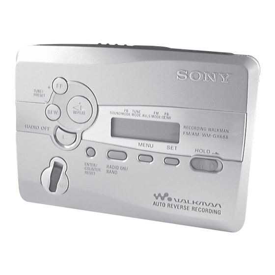
Photo: WM-GX688
SPECIFICATIONS
: 87.5 ~ 108 MHz (Other Models)
: 531 ~ 1 602 kHz (Other Models)
Model Name Using Similar Mechanism
Tape Transport Mechanism Type
Dimensions (w/h/d)
Approx. 108.4 × 77.7 × 23.0 mm
× 3
×
3
1
29
(4
⁄
⁄
⁄
inches)
8
8
32
Mass
Approx. 148 g (5.3 oz)
Supplied accessories
Battery case (1)
Stereo headphones or earphones with
remote control (1)
Battery charger (1)
AC plug adaptor (1) (Saudi Arabian,
Tourist model)
Rechargeable battery (NC-6WM, 1.2 V,
600 mAh, Ni-Cd) (1)
Rechargeable battery carrying case (1)
Carrying pouch (1)
Stereo microphone (1)
Design and specifications are subject to
change without notice.
RADIO CASSETTE-CORDER
US Model
AEP Model
WM-GX680
E Model
Tourist Model
WM-GX688
Chinese Model
WM-GX680/GX688
WM-GX677
MF-WMGX670-162
Advertisement
Table of Contents

Related Manuals for Sony WM-GX680


Summary of Contents for Sony WM-GX680
- Page 1 Microphone (MIC) jack Design and specifications are subject to General change without notice. Power requirements 1.5 V Rechargeable battery One R6 (size AA) battery RADIO CASSETTE-CORDER Sony Corporation 9-873-034-12 2002A1600-1 Personal Audio Company © 2002.1 Published by Sony Engineering Corporation...
-
Page 2: Table Of Contents
LIST ARE CRITICAL TO SAFE OPERATION. REPLACE THESE circuit board (within 3 times). COMPONENTS WITH SONY PARTS WHOSE PART NUMBERS • Be careful not to apply force on the conductor when soldering APPEAR AS SHOWN IN THIS MANUAL OR IN SUPPLEMENTS or unsoldering. -
Page 3: Service Note
Rotation of the idler gear (A) (S side) is detected using the photo- Connect square wave or sine wave to resistor (R43). (See reflector (PH1) in the WM-GX680/688. PH1 is located on the MAIN illustration below.) board, therefore the rotation of the idler gear (A) (S side) cannot be Press the p switch (S3) to enter the STOP mode. - Page 4 [ Slider (NR) ] [ Tape drive mechanism ] Tape drive mechanism in PLAY mode Gear (NR) (FWD : Left side REV : Right side) Idler Gear Idler Gear (A)(S side) Slider (NR) (A)(T side) Gear Gear (REEL)(S side) (REEL)(T side) Motor Pulley Cam Gear F side R side...
-
Page 5: General
SECTION 2 GENERAL This section is extracted from instruction manual. • LOCATION OF CONTROLS REW (AMS) FF (AMS) Y•REPEAT Y•x iREMOTE Plug in firmly. HOLD HOLD TUNE/PRESET + RADIO ON/ TUNE/PRESET – RADIO ON/BAND BAND•OFF RADIO OFF MENU PRESET + ENTER PRESET –... -
Page 6: Disassembly
SECTION 3 DISASSEMBLY Note : Disassemble the unit in the order as shown below. Case assy Lid block assy, cassette Ornament, reel Main board Motor Holder (F) Lever (N)/(R) assy, Head, magnetic Belt (M601) assy pinch (HP901) Note : Follow the disassembly procedure in the numerical order given. 3-1. -
Page 7: Belt
3-2. BELT 3 Belt 2 Terminal board (Battery ’) Belt threading Belt 1 Remove solder from the battery terminal board. 3-3. LID BLOCK ASSY, CASSETTE 5 Lid block assy, cassette 2 Two screws (M1.4 × 2.0) 1 Screw (M1.4 × 2.0) 4 Shaft 3 Open the cassette lid —... -
Page 8: Ornament, Reel
3-4. ORNAMENT, REEL 1 Ornament, reel Note: Remove the assembly while removing the three claws and boss carefully. Claw Claw 3-5. MAIN BOARD 6 Screw (B1.7 × 3) 8 Remove soldering tapping 2 Screw (M1.4) (two points) from plunger solenoid. 5 Screw (B1.7 ×... -
Page 9: Motor (M601)
3-6. MOTOR (M601) 1 Two screws (M1.4) Toothed lock 2 Motor (M601) 3-7. HOLDER (F) ASSY 4 Screw (M1.4) 7 Bracket (cassette) assy 5 Lever (S), lock 8 Flexible board 2 Shaft 9 Remove the holder (F) assy in the direction of the arrow. -
Page 10: Lever (N)/(R) Assy, Pinch
3-8. LEVER (N) / (R) ASSY, PINCH Claw 2 Remove the lever (N) assy, pinch in the direction of the arrow. Note: Be careful of the claw Claw 1 Remove the lever (R) assy, pinch in the direction of the arrow. Note: Be careful of the claw 3-9. -
Page 11: Mechanical Adjustment
SECTION 4 SECTION 5 MECHANICAL ADJUSTMENT ELECTRICAL ADJUSTMENT PRECAUTION PRECAUTION Clean the following parts with a denatured-alcohol-moistened Specified voltage : 1.3 V (DC) swab: Switch and control position record/playback/erase head pinch roller MENU switch rubber belts capstan HOLD : OFF Demagnetize the record/playback/erase head with a head : MAX demagnetizer. - Page 12 FM VCO Adjustment TUNER SECTION 0dB=1µV Procedure : FM RF signal [AM] generator BAND switch : AM 0.01µF AM RF signal to ANT (TP1) generator Put the lead-wire antenna close to Carrier frequency : 98MHz the set. Modulation : no modulation Output level : 0.1V (100dB) 30% amplitude modulation by 400Hz 1.
-
Page 13: Diagrams
SECTION 6 DIAGRAMS 6-1. BLOCK DIAGRAM FM VCO RV301 FM RF/MIX IF AMP/MPX IC301(2/2) D201 Q7,14 Q18(1/2) POWER AMP R-CH J701 10.7MHz D101 MIX OUT IF AMP/ PW IN L PW OUT L L-CH BUFFER FM DET D301 Q1,4 PW NF L Q18(2/2) REMOTE BUFFER... - Page 14 WM-GX680/GX688 Note on Schematic Diagram: • Waveform • All capacitors are in µF unless otherwise noted. pF: µµF 20µsec/div 50 WV or less are not indicated except for electrolytics TP32 5V/div and tantalums. • All resistors are in Ω and W or less unless otherwise specified.
- Page 15 WM-GX680/GX688 6-2. SCHEMATIC DIAGRAM (1/3) • See page 15 for Waveform. • See page 23 for IC Block Diagrams. — 16 — — 17 — — 18 —...
-
Page 16: Schematic Diagram (1/3)
WM-GX680/GX688 • See page 15 for Waveform. • See page 23 for IC Block Diagrams. 6-3. SCHEMATIC DIAGRAM (2/3) — 19 — — 20 —... -
Page 17: Schematic Diagram (2/3)
WM-GX680/GX688 • See page 15 for Waveform. • See page 23 for IC Block Diagrams. • See page 29 for IC PIN FUNCTION DESCRIPTION. 6-4. SCHEMATIC DIAGRAM (3/3) — 21 — — 22 —... -
Page 18: Ic Block Diagrams
6-5. IC BLOCK DIAGRAMS TA7371AF-EL IC501 LA3235W IC301 TA2123AF (EL) 36 35 – SYSTEM CONTROL N.C. RF IN VCC2 PW GND – MIC IN L OUT B V REF PW B NF L V REF OUT C C-AMP SW 37 MT TC PW A PW C... -
Page 19: Printed Wiring Board (Side A)
WM-GX680/GX688 6-6. PRINTED WIRING BOARD (SIDE A) J701 REMOTE DATA REMO MAIN BOARD (SIDE A) J501 (PLUG IN POWER) S501 STOP RV301 • Semiconductor Location 1-680-657- Ref. No. Location (11) Ref. No. Location Ref. No. Location Ref. No. Location B-13... -
Page 20: Printed Wiring Board (Side B)
WM-GX680/GX688 6-7. PRINTED WIRING BOARD (SIDE B) MAIN S901 (-1) (-2) BOARD R TUNE TAPE DETECT (SIDE B) DRY BATTERY SIZE "AA" BATTERY PACK (IEC DESIGNATION R6) (Ni-Cd) 1PC 1.5V NC-6WM 1.2V S902 (-2) (-1) PM901 F TUME (BATTERY CASE) -
Page 21: Ic Pin Function Discription
6-8. IC PIN FUNCTION DESCRIPTION • IC3 TC9327AF-612 (EXCEPT Tourist MODEL), TC9327AF-611(Tourist MODEL) Pin No. Pin Name Description COM 1 to 1 to 4 Common terminal. COM 4 5 to 22 S1 to S18 Segment output terminal. DOLBY VCC Dolby control terminal. (L: ON, Hi-imp: OFF) S1/2 CTL Motor speed control terminal. - Page 22 Pin No. Pin Name Description MOTOR DIR MOTOR control terminal. TAPE TAPE detect terminal. (L: ON, H: OFF) REC CTL REC circuit control output. AVLS CTL Terminal for controlling AVLS (when ON=H). BST CTL Tone control terminal (L: normal, Hi-imp: MEGA BASS). RV CTL Revive control terminal.
-
Page 23: Exploded Views
Ver 1.1 2001. 1 SECTION 7 EXPLODED VIEWS NOTE: • -XX, -X mean standardized parts, so they may • The mechanical parts with no reference number • Abbreviation have some differences from the original one. in the exploded views are not supplied. CH : Chinese model. -
Page 24: Mechanism Deck Block
7-2. MECHANISM DECK BLOCK (MF-WMGX670-162) M601 PM901 HP901 Ref. No. Part No. Description Remarks Ref. No. Part No. Description Remarks X-3377-038-1 HOLDER (F) ASSY (/M) X-3377-584-1 CHASSIS ASSY (F) X-3377-228-1 LEVER (R) ASSY, PINCH 3-010-274-02 TABLE, REEL 3-046-789-01 SPRING (HDA) 3-010-954-01 SPRING (BT), COMPRESSION X-3377-227-1 LEVER (N) ASSY, PINCH 3-029-282-01 GEAR(Y) -
Page 25: Electrical Parts List
SECTION 8 MAIN ELECTRICAL PARTS LIST NOTE: • Due to standardization, replacements in the • RESISTORS • Abbreviation parts list may be different from the parts All resistors are in ohms. CH : Chinese model. specified in the diagrams or the components METAL: metal-film resistor EA : Saudi Arabia model. - Page 26 MAIN Ref. No. Part No. Description Remarks Ref. No. Part No. Description Remarks C301 1-119-663-11 TANTAL. CHIP 47uF 20.00% 2.5V C539 1-164-315-11 CERAMIC CHIP 470PF 5.00% 50V C302 1-107-815-11 TANTAL. CHIP 2.2uF 20.00% 4V C540 1-115-416-11 CERAMIC CHIP 0.001uF 5.00% 25V C303 1-162-970-11 CERAMIC CHIP 0.01uF...
- Page 27 Ver 1.2 2002. 01 MAIN Ref. No. Part No. Description Remarks Ref. No. Part No. Description Remarks < FERRITE BEAD > < TRANSISTOR > 1-500-445-21 FERRITE 8-729-037-89 TRANSISTOR 2SC4627J-C(TX).SO 1-500-445-21 FERRITE 8-729-028-69 TRANSISTOR 2SC4655-BC(TX) 1-500-445-21 FERRITE 8-729-037-89 TRANSISTOR 2SC4627J-C(TX).SO 1-500-245-11 FERRITE 8-729-037-89 TRANSISTOR 2SC4627J-C(TX).SO 1-410-997-31 INDUCTOR...
- Page 28 MAIN Ref. No. Part No. Description Remarks Ref. No. Part No. Description Remarks 1-216-817-11 METAL CHIP 1/16W 1-216-833-11 METAL CHIP 1/16W 1-216-845-11 METAL CHIP 100K 1/16W 1-216-833-11 METAL CHIP 1/16W 1-216-853-11 METAL CHIP 470K 1/16W 1-216-845-11 METAL CHIP 100K 1/16W 1-216-817-11 METAL CHIP 1/16W 1-216-853-11 METAL CHIP...
- Page 29 Ver 1.1 2001. 1 MAIN Ref. No. Part No. Description Remarks Ref. No. Part No. Description Remarks R504 1-216-789-11 METAL CHIP 1/16W 1-572-467-21 SWITCH, PUSH (1 KEY)(REC) R505 1-216-835-11 METAL CHIP 1/16W S501 1-692-605-11 SWITCH, SLIDE (ISS) R506 1-216-835-11 METAL CHIP 1/16W R507 1-216-827-11 METAL CHIP...
- Page 30 WM-GX680/GX688 Ver 1.1 2001. 1 MAIN Ref. No. Part No. Description Remarks 3-222-161-21 MANUAL, INSTRUCTION (ENGLISH,RUSIIAN)(AEP,CEV) 3-222-161-31 MANUAL, INSTRUCTION (SPANISH,PORTUGUESE)(US,AEP) 3-222-161-41 MANUAL, INSTRUCTION (GERMAN,ITALIAN)(AEP) 3-222-161-51 MANUAL, INSTRUCTION (FRENCH,DUTCH)(AEP) 3-222-161-61 MANUAL, INSTRUCTION (SWEDISH,FINNISH)(AEP) 3-222-162-01 MANUAL, INSTRUCTION (JAPANESE,ENGLISH,CHINESE,KOREAN)(JE) 3-222-162-11 MANUAL, INSTRUCTION (ENGLISH,ARABIC) (GX688:CH,EA)
- Page 31 WM-GX670/GX674 MEMO...
- Page 32 WM-GX680/GX688 REVISION HISTORY Clicking the version allows you to jump to the revised page. Also, clicking the version at the upper right on the revised page allows you to jump to the next revised page. Ver. Date Description of Revision 2000.11...