Table of Contents
Advertisement
Quick Links
SERVICE
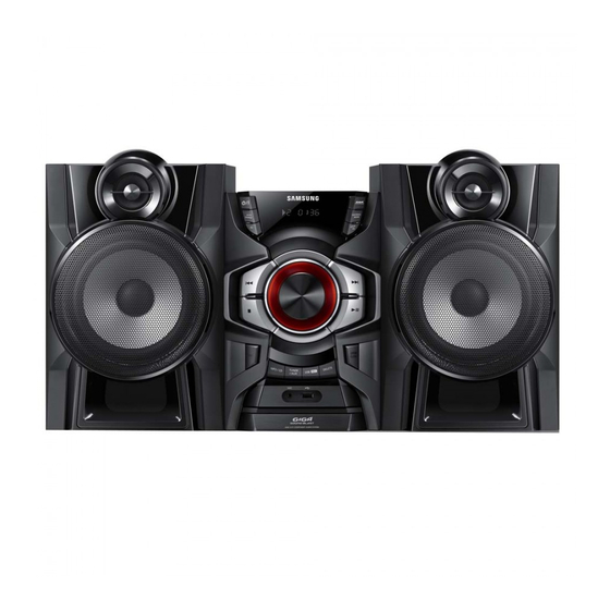
MINI-Compact System
MX-F730
Refer to the service manual in the GSPN (see the rear cover) for more information.
MINI-Compact System
Model Name
Model Code
MANUAL
1. Precaution
2. Product Specification
3. Disassembly and Reassembly
4. Troubleshooting
5. PCB Diagram
6. Schematic Diagram
MX-F730
MX-F730/ZD
Contents
Advertisement
Table of Contents

Related Manuals for Samsung MX-F730


Summary of Contents for Samsung MX-F730
- Page 1 MINI-Compact System Model Name MX-F730 Model Code MX-F730/ZD SERVICE MANUAL MINI-Compact System Contents 1. Precaution 2. Product Specification 3. Disassembly and Reassembly 4. Troubleshooting 5. PCB Diagram 6. Schematic Diagram MX-F730 Refer to the service manual in the GSPN (see the rear cover) for more information.
-
Page 2: Table Of Contents
Pin Connection ......................5 − 10 5.7. SMPS PCB Bottom ........................5 − 11 Schematic Diagram ........................... 6 − 1 6.1. Overall Block Diagram ......................6 − 1 6.2. FRONT ..........................6 − 2 Copyright© 1995-2013 SAMSUNG. All rights reserved. - Page 3 MAIN-3..........................6 − 5 6.5.1. Test Point Wave Form ....................6 − 6 6.6. MAIN-4..........................6 − 7 6.7. MAIN-5..........................6 − 8 6.8. SMPS-1 ..........................6 − 9 6.9. SMPS-2 ..........................6 − 10 Copyright© 1995-2013 SAMSUNG. All rights reserved.
-
Page 4: Precaution
TES T ALL EXPO S ED METAL SU RFACES 2-WIRE CORD ALSO TES T WITH PLUG REVER S ED (US ING AC EARTH ADAPTER P LUG GROUND AS R EQ UIRED) Figure 1.1 AC Leakage Test Copyright© 1995-2013 SAMSUNG. All rights reserved. - Page 5 A replacement part that does not have the same safety characteristics as the original might create shock, fire or other hazards. Copyright© 1995-2013 SAMSUNG. All rights reserved.
-
Page 6: Servicing Precautions
CAUTION First read the “Safety Precautions” section of this manual. If some unforeseen circumstance creates a conflict between the servicing and safety precautions, always follow the safety precautions. Copyright© 1995-2013 SAMSUNG. All rights reserved. -
Page 7: Precautions For Electrostatically Sensitive Devices (Esds)
8) Minimize body motions when handling unpackaged replacement ESDs. Motions such as brushing clothes together, or lifting a foot from a carpeted floor can generate enough static electricity to damage an ESD. Copyright© 1995-2013 SAMSUNG. All rights reserved. -
Page 8: Product Specification
CD Ripping (Able to ripping while listening) • New Bass Sound System (Called GIGA Sound) • Connectivity • • ■ Disc • Type : 1 Tray • Compatible DVD / Divx (Only MX-F730D), MP3, CD/CD-R, RW, WMA Copyright© 1995-2013 SAMSUNG. All rights reserved. -
Page 9: Specifications
Input sensitivity (AUX) 800 mV NOTE • Samsung Electronics Co., Ltd reserves the right to change the specifications without notice. • Weight and dimensions are approximate. • Design and specifications are subject to change without prior notice. • For the power supply and Power Consumption, refer to the label attached to the product. -
Page 10: Specifications Analysis
FM / RDS FM/AM FM/AM, RDS (RUSSIA ONLY) FM/AM 45 KEY 45 KEY 45 KEY REMOTE KEY DUAL VOLTAGE 3.5 OHM 3.5 OHM 4 OHM IMPENDANCE O : Feature Included X : Not Included Copyright© 1995-2013 SAMSUNG. All rights reserved. -
Page 11: Accessories
2. Product Specification 2.4. Accessories 2.4.1. Supplied Accessories Accessories Item Item code Batteries(AAA) 4301-000121 TUNER/AUX Remote Control AH59-02531A REP EAT AUTO CHANGE REP EAT GIGA User’s Manual AH68-02604L FM/AM Antenna AH42-00036A (Optional) Copyright© 1995-2013 SAMSUNG. All rights reserved. -
Page 12: Disassembly And Reassembly
Description Photo Power on and Open the Deck, Separate CD-Door. Unfasten 4 screws on the 2 side Cover. : BH 3*10 BLACK CAUTION Be careful not to make any scratches as you remove them. Copyright© 1995-2013 SAMSUNG. All rights reserved. - Page 13 3. Disassembly and Reassembly Description Description Photo Unfasten 2 screws on the back Cover. : BH 3*10 BLACK Copyright© 1995-2013 SAMSUNG. All rights reserved.
- Page 14 3. Disassembly and Reassembly Description Description Photo Separate the Front panel Copyright© 1995-2013 SAMSUNG. All rights reserved.
- Page 15 3. Disassembly and Reassembly Description Description Photo Unfasten 5 Screws in SMPS and detach AC-CORD & 15P shield wire. : BH 3*10 WHITE Unfasten 2 screws up the DECK, Separate DECK from MECHA. : BH 3*10 BLACK Copyright© 1995-2013 SAMSUNG. All rights reserved.
- Page 16 3. Disassembly and Reassembly Description Description Photo Unfasten 2 screws and detach DECK wire. : BH 3*10 WHITE Unfasten 10 screws, and then separate the front PCB from Front Panel. : BH 3*10 WHITE Copyright© 1995-2013 SAMSUNG. All rights reserved.
-
Page 17: Deck Disassembly And Reassembly
3. Disassembly and Reassembly 3.2. DECK Disassembly and Reassembly Description Description Photo Separate Tray - Disc from DECK. Copyright© 1995-2013 SAMSUNG. All rights reserved. - Page 18 3. Disassembly and Reassembly Description Description Photo Copyright© 1995-2013 SAMSUNG. All rights reserved.
- Page 19 3. Disassembly and Reassembly Description Description Photo Lift up Holder-Cable, separate Traverse-DECK. Copyright© 1995-2013 SAMSUNG. All rights reserved.
- Page 20 3. Disassembly and Reassembly Description Description Photo Disassemble complete. Holde r-Ca ble Holde r-Ca ble Tra verse- Deck Tra verse- Deck Tra y-dis c Tra y-dis c Holde r-Chuck Holde r-Chuck Copyright© 1995-2013 SAMSUNG. All rights reserved.
-
Page 21: Troubleshooting
4. Troubleshooting 4. Troubleshooting 4.1. Checkpoints by Error Mode Oscilloscope Setting Values Normal Voltage 24 MHz 32.768 KHz Voltage/DIV 1 Vol/DIV 1 Vol/DIV 1 Vol/DIV TIME/DIV 1 uS/DIV 10 ns/DIV 0.1 uS/DIV Copyright© 1995-2013 SAMSUNG. All rights reserved. -
Page 22: No Power
Re fe r to wa ve pa tte rn Ye s ima ge of Fig. 4-1. Che ck pa tte rn or re pla ce MICOM IC. Copyright© 1995-2013 SAMSUNG. All rights reserved. - Page 23 MC-146(32. 768KHZ, 20PPM ) DGND DGND R2001 R2001 TUNER_L TUNER_L 1KOHM 1KOHM TUNER_R TUNER_R TPTX TPTX UART_RX UART_RX S-6415A42-M 3T1U S-6415A42-M 3T1U IC2001 IC2001 DGND DGND /RESET,RESET /RESET,RESET UART_TX UART_TX TUGND TUGND * 6.5. MAIN-3 <Fig. 4-1> Copyright© 1995-2013 SAMSUNG. All rights reserved.
-
Page 24: No Output
ALQ41, ARQ31 & ARQ41(IRF6645) on MAIN P CB. (IRF6645) output s igna l on MAIN P CB. Ye s Re pla ce L2001/L2002. Che ck L2001/L2002. Ye s Che ck L2001/L2002 pa tte rn. Copyright© 1995-2013 SAMSUNG. All rights reserved. -
Page 25: Measures To Be Taken When The Protection Circuit Operates
■ Protection Circuit operates when power problem occurs in the SMPS. Protection Location Pin No. Remark Open Short +5.3 V (2~3#) MX-F730/F730D SMPS PCB +PVDD (+34V) (13&15#) CNM802 +PVDD (10#) P-ON (+5 V) (7#) Copyright© 1995-2013 SAMSUNG. All rights reserved. -
Page 26: Check Amp In Power Protection
L CH 2 kΩ If Measured Resistance is very different from above numbers, There is a Problem. → AMP Part Problem CH S P E AK E R O U T R IGHT LE FT Copyright© 1995-2013 SAMSUNG. All rights reserved. -
Page 27: Micom, Mpeg Initialization & Update
2) When finish the Set will be power off → on automatically. 3) And then the Deck is automatically open. ■ MPEG Reset 1) During “No Disc” Displayed, push the stop Button 5 seconds. After displayed “INITIALIZE” set will power off automatically. Copyright© 1995-2013 SAMSUNG. All rights reserved. -
Page 28: Buyer-Region Code Setting Method
The set is not working properly if you don't insert the region code. • The region code is inserted by the remote control. 1) During “AUX” status. • MX-F730/F730CB : Push the “ENTER” button 10 Second. • MX-F730D : Push the “D” button (blue key) 10 Second. <MX-F730> <MX-F730D>... - Page 29 4. Troubleshooting Table 4.1 MX-F730 Option Table Region Code Buyer Africa Brazil China (semi_mic) Europe Indonesia, Asia, Hongkong Latin American Mexico Philippines Russia (semi_mic) M.E.Asia, Israel, Saudi, Argentina , Uruguay, Turkey (MIC) Taiwan USA, Canada New Zealand, Australia Iran (HACO)
- Page 30 Brazil China (semi_mic) Europe Indonesia, Asia, Hongkong Latin American Mexico Philippines Russia (semi_mic) M.E.Asia, Israel, Saudi, Argentina , Uruguay, Turkey (MIC) Taiwan USA, Canada New Zealand, Australia Iran (HACO) India KOR (for test) 4-10 Copyright© 1995-2013 SAMSUNG. All rights reserved.
-
Page 31: Pcb Diagram
DGND 5 GND DGND 6 5.3V +VFD 7 PS_O N P-O N 8 -PVDD SMPS 9 -VP 10 -PVDD 11 -VFD -VFD 12 GND S GND 13 +PVDD 14 GND S GND 15 +PVDD Copyright© 1995-2013 SAMSUNG. All rights reserved. -
Page 32: Front Pcb Top
5. PCB Diagram 5.2. FRONT PCB Top Copyright© 1995-2013 SAMSUNG. All rights reserved. -
Page 33: Pin Connection
5. PCB Diagram 5.2.1. Pin Connection 1) FCN1 VFD/VOL/Key signal from MAIN Pin No. Signal +VFD -VFD VFD_VP VFD_GND VFD_CE VFD_CLK VFD_DO DN_VOL KEY_AD2 KEY_AD1 DGND REMOCON R5.1V M5.1V AGND MIC_SIG AGND MIC_SENS MIC_SENS AGND DGND Copyright© 1995-2013 SAMSUNG. All rights reserved. -
Page 34: Front Pcb Bottom
5. PCB Diagram 5.3. FRONT PCB Bottom Copyright© 1995-2013 SAMSUNG. All rights reserved. -
Page 35: Main Pcb Top
C N 2 MP IC 2 MIC 1 U IC 3 U IC 1 TP 1 MIC 4 AIC 1 AIC 2 MI C2 MIC 3 U C N 1 C N 1 JIG CN Copyright© 1995-2013 SAMSUNG. All rights reserved. -
Page 36: Pin Connection
MIC_SIG AGND M5.1V R5.1V -VFD REMOCON SGND DGND KEY_AD1 SGND KEY_AD2 DN_VOL VREF VFD_DO VFD_CLK DVD_VR VFD_CE DVD_MPD VFD_GND DVD_LD VFD_VP -VFD VCC_5V +VFD 2) RFCN2 Deck Open/Close Control Pin No. Signal INSW OUTSW Copyright© 1995-2013 SAMSUNG. All rights reserved. -
Page 37: Test Point Wave Form
5. PCB Diagram 5.4.2. Test Point Wave Form Copyright© 1995-2013 SAMSUNG. All rights reserved. -
Page 38: Main Pcb Bottom
5. PCB Diagram 5.5. MAIN PCB Bottom Copyright© 1995-2013 SAMSUNG. All rights reserved. -
Page 39: Smps Pcb Top
5. PCB Diagram 5.6. SMPS PCB Top Comply with the threshold of substances which are specified in 0QA_209 N 8 0 2 Copyright© 1995-2013 SAMSUNG. All rights reserved. -
Page 40: Pin Connection
5. PCB Diagram 5.6.1. Pin Connection 1) CN802 VFD/CD/AMP Voltage Supply Pin No. Signal B-5V A5.3V A5.3V 5.3V PS_ON -PVDD -PVDD -VFD +PVDD +PVDD 5-10 Copyright© 1995-2013 SAMSUNG. All rights reserved. -
Page 41: Smps Pcb Bottom
5. PCB Diagram 5.7. SMPS PCB Bottom Comply with the threshold of substances which are specified in 0QA_209 Copyright© 1995-2013 SAMSUNG. All rights reserved. 5-11... -
Page 42: Schematic Diagram
De c ode r (6 30) PW M Fu nction In pu t Crys ta l Pr o Au dio IR Amp De c ode r Pr e AMP /DAC (7 30) Mic AMP (7 30) Copyright© 1995-2013 SAMSUNG. All rights reserved. -
Page 43: Front
JOG- JOG- DN_VOL DN_VOL VFD_DO VFD_DO VFD_DT VFD_DT VFD_CLK VFD_CLK VFD_CLK VFD_CLK VFD_CE VFD_CE VFD_CE VFD_CE DGND DGND VFD_GND VFD_GND MGND MGND DGND DGND VFD- VFD- VFD- VFD- VFD+ VFD+ VFD+ VFD+ FCN1 FCN1 Copyright© 1995-2013 SAMSUNG. All rights reserved. -
Page 44: Main-1
+37VA +37VA SDZ6V2G SDZ6V2G S_GND S_GND D1001 D1001 SDZ7V5G SDZ7V5G 2.2MF 2.2MF APC3 APC3 SGND SGND TP1001 TP1001 SGNDA SGNDA -37V_PW -37V_PW 2.2MF 2.2MF APC4 APC4 S_GND S_GND -37V -37V -37VA -37VA PVDD-37V PVDD-37V Copyright© 1995-2013 SAMSUNG. All rights reserved. -
Page 45: Main-2
22 0OHM 22 0OHM 4.7OHM 4.7OHM ARD5 ARD5 -37V_PW -37V_PW UR101 UR101 2203-007598 2203-007598 ARR11 ARR11 ARD2 ARD2 1N4148 WS 1N4148 WS 220OHM 220OHM 8.2K/3.3K: 65NS 8.2K/3.3K: 65NS DGND DGND S_GND S_GND 5.6K/4.7K:40NS 5.6K/4.7K:40NS Copyright© 1995-2013 SAMSUNG. All rights reserved. -
Page 46: Main-3
0 OH M 0 OH M 1204-003 347 1204-003 347 4730 4730 OMIT OMIT OMIT OMIT DGND DGND TUGND TUGND 1204-003 345 1204-003 345 4705 4705 OMIT OMIT 0 OH M 0 OH M Copyright© 1995-2013 SAMSUNG. All rights reserved. -
Page 47: Test Point Wave Form
6. Schematic Diagram 6.5.1. Test Point Wave Form Copyright© 1995-2013 SAMSUNG. All rights reserved. -
Page 48: Main-4
TEST MODE 5.25 5.25 141.75 141.75 5.75 5.75 155.25 155.25 S_ L S_ L S_ P_ OPTI ON S_ P_ OPTI ON NORMAL MODE NORMAL MODE 148.5 148.5 TEST MODE TEST MODE DGND DGND Copyright© 1995-2013 SAMSUNG. All rights reserved. -
Page 49: Main-5
USB_EN USB_EN EN/EN# EN/EN# SPI _DO SPI _DO SPI _DI SPI _DI P_ON P_ON SPI _CLK SPI _CLK SPI _CS SPI _CS MPQ4 MPQ4 P_ON P_ON MMDT5210W MMDT5210W USB_FLG USB_FLG DGND DGND DGND DGND Copyright© 1995-2013 SAMSUNG. All rights reserved. -
Page 50: Smps-1
MMBT2222AS MMBT2222AS CM804 CM804 50V/47uF 50V/47uF 6.3*11/WL RM817 RM817 5W 0.06 5W 0.06 Block CY803S CY803S QM902 QM902 2N7002K 2N7002K CY804S CY804S AC BLOCK RM921 RM921 1K(2012) 1K(2012) CY806S CY806S CM923 CM923 50V/10nF(1608) 50V/10nF(1608) Copyright© 1995-2013 SAMSUNG. All rights reserved. -
Page 51: Smps-2
2N7002K 2N7002K 1K(1608) 1K(1608) A+5.3V CS 904 CS 904 Block 25V/1uF(1608) 25V/1uF(1608) QS 902 QS 902 ICS 901 ICS 901 2N7002K 2N7002K TL431G-AE2-R TL431G-AE2-R RS 914 RS 914 1K(2012) 1K(2012) CY805S CY805S BLOCK Copyright© 1995-2013 SAMSUNG. All rights reserved. 6-10... - Page 52 E.Asia, W.Asia, https://gspn2.samsungcsportal.com China, Japan N.America, S.America https://gspn3.samsungcsportal.com This Service Manual is a property of Samsung Electronics Co.,Ltd. © 2013 Samsung Electronics Co.,Ltd. Any unauthorized use of Manual can be punished under All rights reserved. applicable International and/or domestic law.