Advertisement
Quick Links
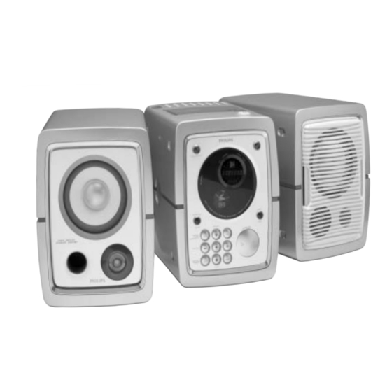
Micro System
Service
Service
Service
Service
Service
Service Manual
©
Copyright 2002 Philips Consumer Electronics B.V. Eindhoven, The Netherlands
All rights reserved. No part of this publication may be reproduced, stored in a retrieval system
or transmitted, in any form or by any means, electronic, mechanical, photocopying, or otherwise
without the prior permission of Philips.
Published by SL 0326 Service Audio
Version 1.0
TABLE OF CONTENTS
Location of PCBs & Version Variations ...................... 1-2
Technical Specifications ............................................. 1-3
Measurement setup .................................................... 1-4
Service Aids, Safety Instruction, etc. .......................... 1-5
Preparations & Controls ............................................. 1-7
Disassembly Instructions ............................................... 2
Set Block diagram ......................................................... 3
Set Wiring diagram ........................................................ 4
Key Board ...................................................................... 5
Power Board .................................................................. 6
Tuner Board ................................................................... 7
MCU & VCD Board ........................................................ 8
Diode & Connection Board ............................................ 9
Main Board .................................................................. 10
Set Mechanical Exploded View & Parts List ............... 11
Printed in The Netherlands
Subject to modification
MC-V320/
Page
CLASS 1
LASER PRODUCT
GB
21M
3140 785 32540
Advertisement

Related Manuals for Philips MC-V320/21M


Summary of Contents for Philips MC-V320/21M
- Page 1 LASER PRODUCT © Copyright 2002 Philips Consumer Electronics B.V. Eindhoven, The Netherlands All rights reserved. No part of this publication may be reproduced, stored in a retrieval system or transmitted, in any form or by any means, electronic, mechanical, photocopying, or otherwise without the prior permission of Philips.
- Page 2 LOCATION OF PRINTED CIRCUIT BOARDS & VERSION VARIATIONS Type/Versions MC-V320 Features & /21M Board in used RDS function ECO Standby Aux Input Digital Coaxial Out Line Out Subwoofer Out Headphone Out AC Voltage Selector Non-Cenelec Tuner Cenelec Tuner...
- Page 3 SPECIFICATIONS GENERAL: Mains voltage AMPLIFIER: Output power (6Ω, 1kHz, 10% THD) : 2X18W : 120V / 230V ±15% Switchable Frequency response within -3dB : 60Hz-14kHz Mains frequency Digital Sound Control (DSC) : Optimal,Classic,Jazz, Rock : 50/60Hz Power consumption : ON/OFF Incredible Surround (IS) : ON/OFF : <...
- Page 4 MEASUREMENT SETUP Tuner FM Bandpass LF Voltmeter 250Hz-15kHz e.g. PM2534 e.g. 7122 707 48001 RF Generator e.g. PM5326 S/N and distortion meter e.g. Sound Technology ST1700B Use a bandpass filter to eliminate hum (50Hz, 100Hz) and disturbance from the pilottone (19kHz, 38kHz). Tuner AM (MW,LW) Bandpass LF Voltmeter...
- Page 5 SERVICE AIDS Service Tools: ESD Equipment: Universal Torx driver holder ........4822 395 91019 Anti-static table mat - large 1200x650x1.25mm ... 4822 466 10953 Torx bit T10 150mm ..........4822 395 50456 Anti-static table mat - small 600x650x1.25mm ..4822 466 10958 Torx driver set T6 - T20 .........
- Page 6 WAARSCHUWING WARNING Alle IC’s en vele andere halfgeleiders zijn All ICs and many other semi-conductors are gevoelig voor electrostatische ontladingen susceptible to electrostatic discharges (ESD). (ESD). Careless handling during repair can reduce life Onzorgvuldig behandelen tijdens reparatie kan drastically. de levensduur drastisch doen verminderen. When repairing, make sure that you are Zorg ervoor dat u tijdens reparatie via een connected with the same potential as the mass...
- Page 7 PREPARATIONS AND CONTROLS...
- Page 8 PREPARATIONS AND CONTROLS...
- Page 9 PREPARATIONS AND CONTROLS...
- Page 10 1-10 PREPARATIONS AND CONTROLS...
- Page 11 1-11 TROUBLESHOOTING...
- Page 12 1-12 TROUBLESHOOTING...
- Page 13 DISASSEMBLY INSTRUCTIONS B1 (x4) A. To remove Brand Rim Left & Right B. To remove Top Cabinet C. To remove Bottom Cabinet D. To remove Tape Deck E. To remove Left & Right Metal Side Bars B2 (x4) F. To remove CD Bracket G.
- Page 15 SET BLOCK DIAGRAM LCD DRIVE IC HT1622 TO POWER TMP87EP26F SUPPLY HEADPHONE OUT AM ANT TO CASS DECK AM IF AM OSC POWER IC 101 AN17830A TA2149BN TU-L TDA T468D FUNCTION IC TU-R PRE-AMP NJM4556AM FM RF 9257F STP16 P/B-R N106 BA316N P/B-L...
- Page 16 SET WIRING DIAGRAM...
- Page 17 HT1622 Block Diagram D i s p l a y R A M O S C I C o n t r o l C O M 0 a n d T i m i n g C O M 7 KEY BOARD C i r c u i t L C D D r i v e r /...
- Page 18 CIRCUIT DIAGRAM - FRONT BOARD...
- Page 19 LAYOUT DIAGRAM - FRONT BOARD LAYOUT DIAGRAM - FRONT BOARD COMPONENT SIDE SMD SIDE...
- Page 20 ELECTRICAL PARTSLIST - KEY BOARD - MISCELLANEOUS - CN901 9965 000 18230 CONN 16P H P=1.0 LCD901 9965 000 18252 LCD MC320 LED901 9965 000 19727 LED RED LED902 9965 000 19727 LED RED LED903 9965 000 18304 LED BT-H203D-31 RED LED904 9965 000 18304 LED BT-H203D-31 RED LED905...
- Page 21 POWER BOARD TABLE OF CONTENTS CircuitDiagram .............. 6-2 PCB Layout ..............6-3 Electrical PartsList............6-4...
- Page 22 CIRCUIT DIAGRAM...
- Page 23 POWER PCB LAYOUT...
- Page 24 ELECTRICAL PARTSLIST - POWER BOARD - MISCELLANEOUS - CN701 9965 000 19724 CON BM V 10P M 2.5 EHB F701 9965 000 19725 FUSE 1.6A TSD1.6A 250V /21 F703 9965 000 18246 FUSE 125MA TAPPING F704 9965 000 18247 FUSE 6.3A TAPPING F705 9965 000 18248 FUSE 3.15A TAPPING...
- Page 25 TUNER BOARD TABLE OF CONTENTS IC Block Diagram ............. 7-2 to 7-7 Circuit Diagram_Non Cenelec ............ 7-8 Layout Diagram-Component_Non Cenelec ....... 7-9 Layout Diagram-SMD_Non Cenelec .......... 7-9 Electrical parts list ..............7-10...
- Page 26 AM / FM TUNER IC AM / FM TUNER IC TA2149BN TA2149BN BLOCK DIAGRAM Pins Description...
- Page 27 AM / FM TUNER IC AM / FM TUNER IC TA2149BN TA2149BN Pins Description Pins Description...
- Page 28 AM / FM TUNER IC AM / FM TUNER IC TA2149BN TA2149BN Pins Description Pins Description...
- Page 29 RDS/RBDS DECODER RDS/RBDS DECODER BU1924F BU1924F Pins Description BLOCK DIAGRAM Pin No. Symbol Pin name Functions Input/Output type QUAL Demodulator quality Good data: High, bad data : Low Type C RDATA Demodulator data Refer to output data timing Vref Reference voltage 1/2 V (refer to input/output circuits) Type E...
- Page 30 DIGITAL TUNING IC DIGITAL TUNING IC TC9257F TC9257F IC BLOCK DIAGRAM...
- Page 31 DIGITAL TUNING IC TC9257F Pins Description...
- Page 32 CIRCUIT DIAGRAM - TUNER BOARD (NON CENELEC)
- Page 33 LAYOUT DIAGRAM - TUNER BOARD (NON CENELEC) LAYOUT DIAGRAM - TUNER BOARD (NON CENELEC) COMPONENT SIDE COPPER SIDE...
- Page 34 7-10 7-10 ELECTRICAL PARTSLIST - TUNER BOARD (NON CENENLEC) - MISCELLANEOUS - - IC & TRANSISTORS - CN102 9965 000 18259 AM ANT TERMINAL 2P Q120 4822 130 42804 BC817-25 CN105 9965 000 18233 CONN 13P P=1.25 V Q121 4822 130 42804 BC817-25 J101 9965 000 11365 FM ANTENNA SOCKET Q122...
- Page 35 MCU & VCD BOARD TABLE OF CONTENTS IC Information ..............8-2 to 8-10 Circuit Diagram ................. 8-11 Layout Diagram-Component ............ 8-12 Layout Diagram-SMD ............... 8-13 Electrical parts list ..............8-14...
- Page 36 MICROPROCESSOR MICROPROCESSOR TMP87EP26F TMP87EP26F BLOCK DIAGRAM PINS DESCRIPTION...
- Page 37 MICROPROCESSOR POWER DRIVER IC TA2092N TMP87EP26F PINS DESCRIPTION...
- Page 38 VIDEO CD/DVD COMPANION PROCESSOR VIDEO CD/DVD COMPANION PROCESSOR ES3207 ES3207 PINOUT PIN DESCRIPTION Name Number Definition Transmit audio data input. 79 78 77 76 75 74 73 72 71 70 69 68 67 66 65 64 63 62 61 60 59 58 57 56 55 54 53 52 DSC_D7 VSSA TBCK...
- Page 39 VIDEO CD PROCESSOR VIDEO CD PROCESSOR ES3210 ES3210 ES3210 PINOUT PIN DESCRIPTION (Continued) Name Number Definition PCLK Pixel clock qualifier in for screen video interface. AUX[7:0] 54:52, 49:45 Auxiliary control pins (AUX0 and AUX1 are open collectors). LD[7:0] 62:55 RISC interface data bus. LWR# RISC interface write enable (active low).
- Page 40 DIGITAL SERVO PROCESSOR TC9462F BLOCK DIAGRAM...
- Page 41 DIGITAL SERVO PROCESSOR DIGITAL SERVO PROCESSOR TC9462F TC9462F PINS DESCRIPTION PINS DESCRIPTION...
- Page 42 DIGITAL SERVO PROCESSOR DIGITAL SERVO PROCESSOR TC9462F TC9462F PINS DESCRIPTION PINS DESCRIPTION...
- Page 43 E2PROM DRAM W27C020 T224162B28S PIN CONFIGURATIONS BLOCK DIAGRAM OUTPUT CONTROL BUFFER CORE DECODER ARRAY 32-pin DIP PIN DESCRIPTION SYMBOL DESCRIPTION Address Inputs A0−A17 Q0−Q7 Data Inputs/Outputs Chip Enable Output Enable Program Enable Program/Erase Supply Voltage Power Supply Ground...
- Page 44 8-10 8-10 MICROPROCESSOR TA2153FN BLOCK DIAGRAM...
- Page 45 8-11 8-11 CIRCUIT DIAGRAM - MCU & VCD BOARD...
- Page 46 8-12 8-12 LAYOUT DIAGRAM - MCU & VCD BOARD COMPONENT SIDE...
- Page 47 8-13 8-13 LAYOUT DIAGRAM - MCU & VCD BOARD SMD SIDE...
- Page 48 8-14 8-14 ELECTRICAL PARTSLIST - VCD MCU BOARD - MISCELLANEOUS - - DIODES - CN1001 9965 000 20205 CONN BASE 3P D405 4822 130 83883 FR202 CN1002 9965 000 20206 CONNECTOR BASE 2P D406 4822 130 83883 FR202 CN301 9965 000 18230 CONN 16P H P=1.0 ZD401 4822 130 83206 BZX79-B5V6 CN302...
- Page 49 DIODE PCB CIRCUIT DIAGRAM DIODE & CONNECTION BOARDS TABLE OF CONTENTS Diode Board - Circuit Diagram ........9 - 1 Diode Board - Layout Diagram........9 - 1 Conn. Board - Circuit Diagram ........9 - 2 Conn. Board - Layout Diagram........9 - 3 DIODE PCB LAYOUT DIAGRAM Electrical Parts List ............
- Page 50 CONNECTION PCB CIRCUIT DIAGRAM...
- Page 51 CONNECTION PCB LAYOUT DIAGRAM...
- Page 52 ELECTRICAL PARTSLIST - DIODE BOARD ELECTRICAL PARTSLIST - CONNECTION BOARD - DIODES - - MISCELLANEOUS - 9965 000 19770 DIODE 1N5402GW F20 CN403 9965 000 18229 CONN P=1.5 H 6PIN 9965 000 19770 DIODE 1N5402GW F20 CN404 9965 000 18230 CONN 16P H P=1.0 CN405 9965 000 18231 CONN 22P P=1.0 H 9965 000 19770 DIODE 1N5402GW F20...
- Page 53 10-1 10-1 MAIN BOARD TABLE OF CONTENTS IC Block Diagram ............10-2 to 10-3 Circuit Diagram - Main Part ............10-4 Circuit Diagram - Tape Part ............. 10-5 Component Layout - Main PCB ..........10-6 SMD Layout - Main PCB ............10-7 Electrical Parts List ..............
- Page 54 10-2 10-2 TAPE HEAD SWITCHING IC IC BLOCK DIAGRAM BA3126N TDA7468 Block diagram TDA7468 INTERNAL BLOCK DIAGRAM TDA7468 VOLUME II VOLUME I TREBLE BASS POWER SUR. SUPPLY LEFT LEFT LEFT LEFT BASS ALC SOURCE SELECTOR LOGIC IIC BUS Internal circuit configuration VOLUME I VOLUME II...
- Page 55 10-3 10-3 IC BLOCK DIAGRAM IC BLOCK DIAGRAM AN17830A TA8142AP CH1-IN CH1-O+ TSD PROT CIRCUIT CH1-O- CH2-IN MUTE CH2-O+ MUTE STBY CH2-O- STBY CIRC...
- Page 56 10-4 10-4 MAIN BOARD - CIRCUIT DIAGRAM...
- Page 57 10-5 10-5 TAPE PART - CIRCUIT DIAGRAM...
- Page 58 10-6 10-6 MAIN PCB - COMPONENT LAYOUT...
- Page 59 10-7 10-7 MAIN PCB - SMD LAYOUT...
- Page 60 10-8 10-8 ELECTRICAL PARTSLIST - MAIN BOARD ELECTRICAL PARTSLIST - MAIN BOARD - IC & TRANSISTORS - - MISCELLANEOUS - - DIODES - CN001 9965 000 20199 WIRE ASS'Y 3PIN D610 4822 130 31878 1N4003G Q801 5322 130 60159 BC846B Q802 4822 130 60373 BC856B CN201...
- Page 61 11-1 11-1 EXPLODED DRAWING (8x) (4x) SCREW LIST : KT2.6 x 6 (11x) KT2.6 x 8 (2x) T3 x 8 T3 x 10 (4x) T3 x 12 T4 x 8 (3x) (1x) (3x) O1 (x2) (4x) (4x) (4x) (2x) (4x) (1x) (2x) (4x)
- Page 62 11-2 11-2 MECHANICAL & ACCESSORIES PARTSLIST 9965 000 20194 CD DOOR LENS 9965 000 20195 IFU MCV320 9965 000 18185 CD CHROME RING 9965 000 11157 FM ANTENNA WIRE 9965 000 20183 CD DOOR PANEL 4822 303 50082 AM LOOP ANTENNA 9965 000 20182 KEY SET FUNCTION 9965 000 20196...