Table of Contents
Advertisement
RX-V495/RX-V495RDS/
HTR-5140/HTR-5140RDS
CONTENTS
TO SERVICE PERSONNEL ........................................... 1
REMOTE CONTROL PANELS ....................................... 1
FRONT PANELS ............................................................. 2
REAR PANELS ........................................................... 3~4
SPECIFICATIONS ....................................................... 5~6
INTERNAL VIEW ............................................................ 7
DISASSEMBLY PROCEDURES .................................... 7
SELF DIAGNOSIS FUNCTION ................................ 8~19
FACTORY PRESET ...................................................... 20
1 0 0 6 5 0
SERVICE MANUAL
IMPORTANT NOTICE
This manual has been provided for the use of authorized YAMAHA Retailers and their service personnel.
It has been assumed that basic service procedures inherent to the industry, and more specifically YAMAHA
Products, are already known and understood by the users, and have therefore not been restated.
WARNING:
Failure to follow appropriate service and safety procedures when servicing this product
may result in personal injury, destruction of expensive components, and failure of the
product to perform as specified. For these reasons, we advise all YAMAHA product
owners that any service required should be performed by an authorized YAMAHA
Retailer or the appointed service representative.
IMPORTANT:
The presentation or sale of this manual to any individual of firm does not constitute
authorization, certification or recognition of any applicable technical capabilities,
or establish a principle-agent relationship of any form.
The data provided is believed to be accurate and applicable to the unit(s) indicated on the cover. The research,
engineering, and service departments of YAMAHA are continually striving to improve YAMAHA products.
Modifications are, therefore, inevitable and specifications are subject to change without notice or obligation
to retrofit. Should any discrepancy appear to exist, please contact the distributor's Service Division.
WARNING:
Static discharges can destroy expensive components. Discharge any static electricity
your body may have accumulated by grounding yourself to the ground buss in the unit
(heavy gauge black wires connect to this buss).
IMPORTANT:
Turn the unit OFF during disassembly and part replacement. Recheck all work before
you apply power to the unit.
AMP ADJUSTMENT ..................................................... 21
TUNER ADJUSTMENT ........................................... 22~25
IC DATA .................................................................. 26~35
DISPLAY DATA ........................................................... 36
BLOCK DIAGRAM .................................................. 37~39
PRINTED CIRCUIT BOARD ................................... 40~57
SCHEMATIC DIAGRAM ......................................... 58~65
PARTS LIST ............................................................ 66~81
REMOTE CONTROL TRANSMITTER ......................... 82
AV RECEIVER
Advertisement
Table of Contents

Related Manuals for Yamaha RX-V495


Summary of Contents for Yamaha RX-V495
-
Page 1: Table Of Contents
SERVICE MANUAL IMPORTANT NOTICE This manual has been provided for the use of authorized YAMAHA Retailers and their service personnel. It has been assumed that basic service procedures inherent to the industry, and more specifically YAMAHA Products, are already known and understood by the users, and have therefore not been restated. -
Page 2: To Service Personnel
RX-V495/RX-V495RDS/HTR-5140/HTR-5140RDS TO SERVICE PERSONNEL 1. Critical Components information. Components having special characteristics are marked and must be replaced with parts having specifications equal to those originally AC LEAKAGE installed. WALL EQUIPMENT TESTER OR 2. Leakage Current Measurement (For 120V Model only). -
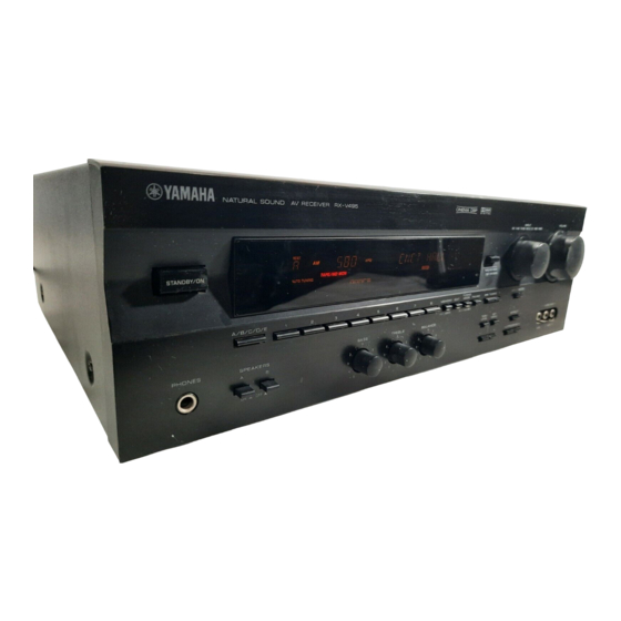
Page 3: Front Panels
RX-V495/RX-V495RDS/HTR-5140/HTR-5140RDS FRONT PANELS RX-V495 (U, C, R, T, A and L models) RX-V495RDS (B and G models) HTR-5140 (U, C, T and A models) HTR-5140RDS (G model) -
Page 4: Rear Panels
RX-V495/RX-V495RDS/HTR-5140/HTR-5140RDS REAR PANELS RX-V495/HTR-5140 U model RX-V495/HTR-5140 C model RX-V495 R model RX-V495/HTR-5140 T model... - Page 5 RX-V495/RX-V495RDS/HTR-5140/HTR-5140RDS RX-V495/HTR-5140 A model RX-V495RDS B model RX-V495RDS/HTR-5140RDS G model RX-V495 L model...
-
Page 6: Specifications
RX-V495/RX-V495RDS/HTR-5140/HTR-5140RDS SPECIFICATIONS Residual Noise(IHF-ANetwork) AUDIO SECTION MAIN L/R, SP OUT 150µV Minimum RMS Output Power Per Channel Channel Separation(Vol. –30dB, EFFECT OFF) (Power Amp. Section) PHONO, Input shorted, 1kHz/10kHz 60dB/55dB MAIN L/R, REAR L/R CD etc, Input 5.1kΩ terminated, 1kHz/10kHz 20Hz to 20kHz, 0.04% THD, 8Ω... - Page 7 RX-V495/RX-V495RDS/HTR-5140/HTR-5140RDS DIMENSIONS VIDEO SECTION Video Signal Type U, C models NTSC R model NTSC/PAL T, A, B, G, L models Video Signal Level 1Vp-p/75Ω Maximum Input Level 1.5Vp-p Signal-to-Noise Ratio 50dB Monitor Output Frequency Response(–3dB) 5Hz~10MHz GENERAL Power Supply U, C, models...
-
Page 8: Internal View
RX-V495/RX-V495RDS/HTR-5140/HTR-5140RDS INTERNAL VIEW 1 POWER TRANSFORMER 1 2 3 4 5 6 2 P.C.B. MAIN (3) 3 P.C.B. OPERATION (7) (R, T models only) 4 P.C.B. OPERATION (3) 5 P.C.B. MAIN (4) 6 P.C.B. MAIN (8) 7 P.C.B. OPERATION (6) 8 P.C.B. -
Page 9: Self Diagnosis Function
SELF DIAGNOSIS FUNCTION 1. PURPOSE AND OPERATION The RX-V495/RX-V495RDS/HTR-5140/HTR-5140RDS has a Self Diagnosis Function to locate a faulty part, if any, by inspecting and taking measurements. There are 11 main items in the diagnostic menu and some of them have sub-menu items as listed below. - Page 10 RX-V495/RX-V495RDS/HTR-5140/HTR-5140RDS 2. BEGINNING AND CANCELLATION (1) STARTING UP THE FUNCTION AND THE DISPLAY After starting up, menu No. 1 is selected. A. How to start diagnostic program Using the front panel keys of the main unit. Plug in the AC power cord to the outlet, and when the main power off condition;...
- Page 11 RX-V495/RX-V495RDS/HTR-5140/HTR-5140RDS FL display at start-up of diagnostic program When the diagnostic program has started, the history (*2) of the protection function (*1) is displayed. If the protection function has been activated in the past, the type and voltage value are displayed. After a few seconds the diagnosis function menu will appear.
- Page 12 RX-V495/RX-V495RDS/HTR-5140/HTR-5140RDS 3. OPERATION AND DISPLAY WHEN STARTING DIAGNOSIS FUNCTION (1) Selection of diagnostic menu The diagnostic menu and the sub-menu can be selected by using the front panel keys of the main unit or the remote control unit. Selection by using the front panel keys The main menu can be changed cyclically by using the "TUNING UP/DOWN"...
- Page 13 RX-V495/RX-V495RDS/HTR-5140/HTR-5140RDS 4. CONTENTS OF DIAGNOSIS FUNCTION This section describes the contents of the self diagnosis function in detail. No.1 ANALOG THROUGH The input is fixed to analog (A/D). There are two submenus. 1 DVD/LD MAIN BYPAS 1. MAIN BYPASS The MAIN L/R signals bypass the analog circuits to be output.
- Page 14 RX-V495/RX-V495RDS/HTR-5140/HTR-5140RDS No.2 DSP THROUGH The input is automatically discriminated by signal detection and switched with priorities AC3>PCM Audio>analog. There are the following three submenus. 2 DVD/LD YSS908SRAM 1. YSS908-SRAM MAIN L/R are input to the DSP via AC3Dav, pass through SRAM, and are then output to all channels without being processed.
- Page 15 RX-V495/RX-V495RDS/HTR-5140/HTR-5140RDS No.3 AC3 THROUGH The input is digital signal only. AC3 (DOLBY DIGITAL) decoding operation is executed, according to the input source. 3 DVD/LD 3T00000001 1. STATUS(BINARY FORM) AC3 (DOLBY DIGITAL) decoded signals are output to each channel via AC3Dav.
- Page 16 RX-V495/RX-V495RDS/HTR-5140/HTR-5140RDS No.5 SPEAKERS SET The input is automatically discriminated by AC3>PCM>analog. There are the following 9 submenu items: The signal from the DSP block is normally in the effect off status for menu items 1-4. For other menu items, the same signal as in 2. DSP THROUGH: YSS908 menu is output.
- Page 17 RX-V495/RX-V495RDS/HTR-5140/HTR-5140RDS No.6 DISPLAY CHECK Check program for FL display. The display status will change as follows with submenu operation. The signal is processed with EFFECT OFF. 6 DVD/LD DISP CHECK Initial display. All segments are turned off All segments are turned on...
- Page 18 RX-V495/RX-V495RDS/HTR-5140/HTR-5140RDS No.9 AD DATA CHECK The A/D conversion values of the main CPU which detects key scan, protection, etc. are displayed in % (100%: 5V). All signal processing before this menu is executed will be held. The keys on the main unit cannot be operated to detect the values of all keys in the K1/K2/K3/K4 and SI.
- Page 19 RX-V495/RX-V495RDS/HTR-5140/HTR-5140RDS No.10 STATUS FROM DSP MICOM The status data from the DSP microprocessor is sequentially displayed in a hexadecimal number. All signal processing before this menu is executed will be held. STATUS 1st 2nd 3rd 4th 10 DVD/LD 0 00000000...
- Page 20 RX-V495/RX-V495RDS/HTR-5140/HTR-5140RDS No.11 CPU VERSION/CHECK SUM/PORT INFO/EXIT DIAG The check sum, version and port setting of main CPU/DSP CPU are displayed. The signal is EFFECT OFF. Operating the submenu will finish self-diagnosis, and ordinary operation mode will be restored. The suffix letter ("B" in the following) of version indication is for compatibility of communications between the main and DSP microprocessors.
-
Page 21: Factory Preset
RX-V495/RX-V495RDS/HTR-5140/HTR-5140RDS FACTORY PRESET All the settings of the system are initialized on shipping. The settings are as follows. INPUT (VIDEO) DVD/LD (DVD/LD) EFFECT LEVEL EFFECT CHANNEL PRESET VALUE CENTER 0 dB RIGHT SURROUND 0 dB LEFT SURROUND 0 dB SUB WOOFER... - Page 22 RX-V495/RX-V495RDS/HTR-5140/HTR-5140RDS Confirmation of Idling Current of Main Amplifier Right after power is turned on, confirm that the voltage across the terminals of R688(Main Lch),R690(Main Rch), R692(Center), R694(Rear Lch), R696(Rear Rch) are between 0.1mVand 5.0mV. If it exceeds 5.0mV, open (cut off) R571 (Main Lch), R577 (Main Rch), R589 (Center), R595 (Rear Lch), R583 (Rear Rch) and reconfirm the voltage again.
-
Page 23: Tuner Adjustment
RX-V495/RX-V495RDS/HTR-5140/HTR-5140RDS TUNER ADJUSTMENT 1. Measuring Instruments Dummy antenna FM signal generator (FM SG) FM dummy antenna Stereo signal generator (SSG) AM signal generator (AM SG) 10Ω 45Ω Distortion meter (DIST. M) RECEIVER FM SG AC Voltmeter (ACVM) (75Ω) (50Ω) DC Voltmeter (DCVM) - Page 24 RX-V495/RX-V495RDS/HTR-5140/HTR-5140RDS FM Adjustment 1. Before Adjustment Set each switch to the following position unless otherwise For dBµ, 1µV=0dBµ applies. specified. Example : 60dBµ=1mV INPUT SELECTOR ..TUNER 100% modulation means that the frequency deviation is TUNING MODE ..... AUTO ±75kHz.
- Page 25 RX-V495/RX-V495RDS/HTR-5140/HTR-5140RDS See page 22 for TP locations & adjustment points. Reception Adjustment Step Adjustment item Signal (ANT IN) Test point Rating frequency point Adjustment of FM ANT (75Ω) 98.1MHz Front end IFT Adjust so that the meter is Pin 16 of IC1 front end IFT 98.1MHz...
- Page 26 RX-V495/RX-V495RDS/HTR-5140/HTR-5140RDS AM Adjustment (This should be done after FM adjustment.) 1. Connection diagram (Measuring instruments) Adjustment of sensitivity. AM loop antenna AM ANT ACVM TUNER AM SG dummy P. C. B. antenna DIST. M Oscilloscope See page 22 for TP locations & adjustment points.
-
Page 27: Ic Data
RX-V495/RX-V495RDS/HTR-5140/HTR-5140RDS IC DATA IC800 : LC87F65C8A (LC876564A-5K19) µ 8 bit -COM S48/PG0 S19/PC3 S49/PG1 S18/PC2 S50/PG2 S17/PC1 S51/PG3 S16/PC0 VDD3 S15/T15 S14/T14 S13/T13 VSS2 S12/T12 VDD2 S11/T11 TOP VIEW S10/T10 S9/T9 S8/T8 S7/T7 P10/SO0 S6/T6 P11/SI0 S5/T5 P12/SCK0 S4/T4 P13/SO1... - Page 28 RX-V495/RX-V495RDS/HTR-5140/HTR-5140RDS IC800 : LC87F65C8A (LC876564A-5K19) µ 8 bit -COM Port Function Port Function Name Name FLA-CLK I/O Flush clock 26 P70/INT0 I Power down detect FLA-I/O I/O Flush input/output 27 P71/INT1 O Full mute (L : ON) FLA-SEL I/O Flush select...
- Page 29 RX-V495/RX-V495RDS/HTR-5140/HTR-5140RDS IC800 : LC87F65C8A (LC876564A-5K19) µ 8 bit -COM Port Function Port Function Name Name 76 S43/PF3 POWER-RY O Power relay 52 S20/PC4 O FL Segment 5 77 S44/PF4 –10dB O –10 dB select (L : –10dB) 53 S21/PC5 O FL Segment 6...
- Page 30 RX-V495/RX-V495RDS/HTR-5140/HTR-5140RDS IC14 : LC87F5164A (LC875164A-5K20) µ 8 bit Sub -COM PWM1 SI2P3 SCK2 P17/PWM P16/PWL VSS3 P15/SCK1 VDD3 P14/SI1 P13/SO1 TOP VIEW P12/SCK0 P11/SI0 P10/SOO P87/AN7 P86/AN6 INTERRUPT CONTROL STANDBY /RES CONTROL CLOCK GENE- RATOR Xtal SERIAL I/O 0 BUS INTERFACE...
- Page 31 RX-V495/RX-V495RDS/HTR-5140/HTR-5140RDS IC14 : LC87F5164A (LC875164A-5K20) µ 8 bit Sub -COM Port Function Port Function Name Name I Receive data from DIR2 PWM0 OL Unconnected /ICDI O Initial clear for DIR2 VDD2 VDD2 +5V +5V power supply /KM1 O Switching DIR2 forced (analog) mode...
- Page 32 RX-V495/RX-V495RDS/HTR-5140/HTR-5140RDS IC3 : YM3436DK (DIR2) Digital Format Interface Receiver 24 26 28 25 17 15 14 13 12 31 EXTW DOM0 SYSTEM CLOCK EXTW DOM1 TIMING DDIN DIM0 SYNC GENERATOR DIM1 D DIN TOP VIEW DATA CLOCK EIAJ (AES/EBU) CONTROLLER...
- Page 33 RX-V495/RX-V495RDS/HTR-5140/HTR-5140RDS IC4 : YSS908-F (AC3Dav) Digital Dolby Pro Logic Decoder +DSP PVSS SDWCK0 SDWCK1 SDBCK0 SDBCK1 SDIA0 SDOB0 SDIA1 SDOB1 RAMA1 SDOB2 RAMA0 RAMA7 RAMWEN RAMA8 RAMOEN RAMA9 TOP VIEW IPORT7 OPORT7 IPORT6 OPORT6 IPORT5 OPORT5 IPORT4 OPORT4 IPORT3 OPORT3...
- Page 34 RX-V495/RX-V495RDS/HTR-5140/HTR-5140RDS IC4 : YSS908-F (AC3Dav) Digital Dolby Pro Logic Decoder +DSP Name Function PVDD +5V power supply RAMCEN RAM chip enable output terminal, connected to external 1M SRAM chip enable RAMA16 RAM address output terminal 16, connected to external 1M SRAM address...
- Page 35 RX-V495/RX-V495RDS/HTR-5140/HTR-5140RDS IC4 : YSS908-F (AC3Dav) Digital Dolby Pro Logic Decoder +DSP Name Function +3V power supply AC3DATA AC-3 data output terminal, AC-3 bit stream data detect CRC output terminal (normally unconnected) MUTE Mute output terminal, output data mute detect KARAOKE...
- Page 36 RX-V495/RX-V495RDS/HTR-5140/HTR-5140RDS IC5 : M5M51288BKJ-20LTEL (1M SRAM) 131072-word x 8 bit High Speed Static RAM 131072-word x 8 bit MEMORY ARRAY (512-row X 2048-column) 2048 TOP VIEW COLUMN I/O COLUMN ADDRESS /CE1 DECODER COLUMN INPUT BUFFER /CE1 CHIP SELECT WRITE CONTROL...
-
Page 37: Display Data
DSP-R495/RX-V495/RX-V495RDS/HTR-5140/HTR-5140RDS DISPLAY DATA BLOCK DIAGRAM (1/2) V800 : 16-BT-59GK (V2421800) PATTERN AREA • PIN CONNECTION Pin No. CONNECTION Pin No. CONNECTION Pin No. NOTE 1) F1, F2 ..Filament 2) NP ....No pin CONNECTION 3) NC ....No connection 4) DL .... - Page 38 DSP-R495/RX-V495/RX-V495RDS/HTR-5140/HTR-5140RDS BLOCK DIAGRAM (2/2) MAIN PHONES MAIN SELECTOR POWER AMP LEVEL IC102 VR401 IC10A IC103 Q506,511,512, IC103 521,529,Q527A/C IC351 IC108B IC401A IC802A INPUT MAIN COAX SELECTOR Q501 DVD/LD IC352 H,P,F Q810 IC103 TONE IC10B TV/DBS IC103 CONTROL RY501 OPTICAL SIGNAL...
-
Page 39: Printed Circuit Board
DSP-R495/RX-V495/RX-V495RDS/HTR-5140/HTR-5140RDS PRINTED CIRCUIT BOARD (Foil side) P. C. B. ASS'Y TUNER LIST Lead & SMD : See page 42~43, PRINTED CIRCUIT BOARD Model Markets Lead Type Lead & SMD There are two types of P. C. B. Assembly Tuner for these models in items of construction of components. - Page 40 DSP-R495/RX-V495/RX-V495RDS/HTR-5140/HTR-5140RDS PRINTED CIRCUIT BOARD (Foil side) P. C. B. ASS'Y TUNER LIST Model Markets Lead & SMD Lead Type Lead Type : See page 40~41, PRINTED CIRCUIT BOARD There are two types of P. C. B. Assembly Tuner for these models in items of construction of components.
- Page 41 DSP-R495/RX-V495/RX-V495RDS/HTR-5140/HTR-5140RDS PRINTED CIRCUIT BOARD (Foil side) P. C. B. DSP P. C. B. DSP TO: INPUT (1) TO: INPUT (3) TO: INPUT (1) LC87F5164A HD74HC02FP YSS908-F YM3436DK AK4526 AK4320 Semiconductor Location Point Point Pin 13 of IC4 Ref. No. Location Ref.
- Page 42 DSP-R495/RX-V495/RX-V495RDS/HTR-5140/HTR-5140RDS B, G models only PRINTED CIRCUIT BOARD (Foil side) P. C. B. OPERATION (1) PTY SEEK – PROGRAM MODE START Semiconductor Location Ref. No. Location D800 B, G D801 models only D802 EFFECT D803 MENU D805 TIME/ LEVEL D806...
- Page 43 DSP-R495/RX-V495/RX-V495RDS/HTR-5140/HTR-5140RDS P. C. B. OPERATION (6) PRINTED CIRCUIT BOARD (Foil side) P. C. B. OPERATION (5) • J, U, C, R and T models SWITCHED 100W MAX. TOTAL P. C. B. OPERATION (3) AC OUTLETS R, T models only J, U, C, R and T Models Semiconductor Location Ref.
- Page 44 DSP-R495/RX-V495/RX-V495RDS/HTR-5140/HTR-5140RDS PRINTED CIRCUIT BOARD (Foil side) P. C. B. MAIN (1) NFRL NFRR –B A, B, G, L only SPRY PRV1 A, B, G, L only W803 W504 TO: MAIN (3) TO: OPERATION (1) W761 W815 TO: MAIN (4) TO: OPERATION (3) P.
- Page 45 DSP-R495/RX-V495/RX-V495RDS/HTR-5140/HTR-5140RDS PRINTED CIRCUIT BOARD (Foil side) P. C. B. MAIN (7) P. C. B. MAIN (6) P. C. B. MAIN ( 3 ) P. C. B. MAIN (4) TO: INPUT (1) TO: MAIN (1) W761 TO: MAIN (1) OPERATION (5) W504 –B2...
- Page 46 DSP-R495/RX-V495/RX-V495RDS/HTR-5140/HTR-5140RDS PRINTED CIRCUIT BOARD (Foil side) P. C. B. INPUT (1) Semiconductor Location Ref. No. Location D101 D102 D103 D104 TO: TUNER TO: DSP TO: DSP IC101 IC102 IC103 IC104 IC105 IC106 IC107 IC108 A, L, B, G only IC109...
- Page 47 DSP-R495/RX-V495/RX-V495RDS/HTR-5140/HTR-5140RDS PRINTED CIRCUIT BOARD (Foil side) P. C. B. INPUT (2) P. C. B. INPUT (3) P. C. B. INPUT (4) TO: INPUT (1) W102 INPUT (1) –12 +12A LFEO W101 LA7956 +12A /VCR TO: DSP VSEL1 VSEL0 TO: INPUT (1)
-
Page 48: Schematic Diagram
DSP-R495/RX-V495/RX-V495RDS/HTR-5140/HTR-5140RDS SCHEMATIC DIAGRAM (INPUT) VIDEO SELECTOR & AMP VCR-IN 11.8 VCR-OUT VIDEO SIGNAL VIDEO TV/DBS DVD/LD MONITOR PIN CONNECTION DIAGRAM OF IC303 : LA7956 Video Switch TRANSISTORS AND IC’s. 2SC1815(Y) LA7956 2SC1740S(R,S) Conditions (RX-V495RDS) → CD • INPUT → minimum(–∞) •... - Page 49 DSP-R495/RX-V495/RX-V495RDS/HTR-5140/HTR-5140RDS SCHEMATIC DIAGRAM (INPUT) TO OPE(4) CB802 VOLUME AMP FRONT L REAR L TO DSP CB6 MAIN L MAIN L MAIN L MAIN L (DSP) (DSP) 11.8 CENTER PHONO(MM) CENTER/SUB WOOFER/FRONT/REAR AMP CENTER EQ AMP 24.0 MAIN L 11.4 MAIN L CENTER -11.5...
- Page 50 DSP-R495/RX-V495RX-V495RDS/HTR-5140/HTR-5140RDS SCHEMATIC DIAGRAM (MAIN) REGULATOR MAIN (1),(2),(5),(6) MAIN POWER AMP 29.0 12.9 43.1 13.5 43.0 43.1(31.8) MAIN POWERAMP MAIN L 43.1(31.8) 42.8 -0.4 MUTE -1.1 -11.5 SPEAKERS -41.3 -42.0 -0.5 -0.5 -1.0 -43.0 -1.1 (-31.8) -43.0 -41.3 MAIN (-31.8) -41.8 MAIN :NOT USED RELAY...
- Page 51 DSP-R495/RX-V495/RX-V495RDS/HTR-5140/HTR-5140RDS SCHEMATIC DIAGRAM (OPERATION) IC801, 802 : NJM2068LD • IC800→See page 26~28, IC DATA Dual OP-Amp – – VIDEO 2 3 4 5 6 RJ-1086-01-0300 AUDIO -23.0 -30.0 OPE(2),(3),(4) TONE CONTROL 11.8 11.8 -20.0 -11.5 SYSTEM & DSP -9.2 CONTROL -27.4...
- Page 52 DSP-R495/RX-V495RX-V495RDS/HTR-5140/HTR-5140RDS SCHEMATIC DIAGRAM (DSP) TO INPUT(3) CB354 DIGITAL L.P.F 3. 1 2. 4 2. 4 DOLBY DIGITAL 11.7 PRO-LOGIC DECODER MAIN L 2. 3 (DSP) 0. 9 ADC/ -11.4 4. 6 2. 4 0. 1 2. 4 11.7 -11.4 Point MUTING Pin 13 of IC3 DSP AMP...
- Page 53 DSP-R495/RX-V495/RX-V495RDS/HTR-5140/HTR-5140RDS Each voltage given here repressents that in the FM (98.1MHz STEREO) reception mode SCHEMATIC DIAGRAM (TUNER) J, U, C, R, T, A and L models but the one in the parentheses ( ) is that in the AM (1080kHz, MAN’L) reception mode.
- Page 54 DSP-R495/RX-V495/RX-V495RDS/HTR-5140/HTR-5140RDS Each voltage given here repressents that in the FM (98.1MHz STEREO) reception mode SCHEMATIC DIAGRAM (TUNER) B, G models but the one in the parentheses ( ) is that in the AM (1080kHz, MAN’L) reception mode. IC1 : LA1266...
-
Page 55: Parts List
RX-V495/RX-V495RDS/HTR-5140/HTR-5140RDS WARNING P ARTS LIST Components having special characteristics are marked and must be replaced with parts having specifications equal to those originally installed. ELECTRICAL PARTS Carbon resistors (1/6W or 1/4W) are not included in the ELECTRICAL PARTS List. For the part Nos. of the carbon resistores,refer to the last page. - Page 56 RX-V495/RX-V495RDS/HTR-5140/HTR-5140RDS P. C. B. DSP Schm Schm PART NO. Description PART NO. Description UR818330 C.EL 330uF 6.3V V3005700 P.C.B. VQ044200 CN.BS.PIN UB245100 C.CE.M.CHP 0.1uF UR818330 C.EL 330uF 6.3V VQ044500 CN.BS.PIN UB245100 C.CE.M.CHP 0.1uF VQ044600 CN.BS.PIN UB245100 C.CE.M.CHP 0.1uF UB245100 C.CE.M.CHP 0.1uF UR818330 C.EL...
- Page 57 RX-V495/RX-V495RDS/HTR-5140/HTR-5140RDS P. C. B. DSP & P. C. B. INPUT Schm Schm PART NO. Description PART NO. Description C122 UA952100 C.MYLAR 100pF IC14 XV260E00 IC LC875164A-5K20 CPU C123 UR837220 C.EL 22uF IC15 XU965A00 IC uPC29M33T-E1 3.3V C124 UR847100 C.EL 10uF VV655300 TR.DGT...
- Page 58 RX-V495/RX-V495RDS/HTR-5140/HTR-5140RDS P. C. B. INPUT Schm Schm PART NO. Description PART NO. Description C104 UA952100 C.MYLAR 100pF 50V(ALBG) C160 UR837100 C.EL 10uF C105 UA952220 C.MYLAR 220pF C161 VJ599100 C.CE.TUBLR 0.1uF C106 UR866220 C.EL 2.2uF C162 VJ599100 C.CE.TUBLR 0.1uF C107 VF467300 C.CE.TUBLR 0.01uF C163 UA952100 C.MYLAR...
- Page 59 RX-V495/RX-V495RDS/HTR-5140/HTR-5140RDS P. C. B. INPUT Schm Schm PART NO. Description PART NO. Description C351 VG278400 C.CE.TUBLR 220pF C435 UR838100 C.EL 100uF C352 VG278400 C.CE.TUBLR 220pF C436 VJ599100 C.CE.TUBLR 0.1uF C353 VG278400 C.CE.TUBLR 220pF D101 VM975300 DIODE.ZENR HZS11B2TD 11V C354 VG278400 C.CE.TUBLR 220pF D102 VM975300 DIODE.ZENR HZS11B2TD 11V...
- Page 60 RX-V495/RX-V495RDS/HTR-5140/HTR-5140RDS P. C. B. INPUT & P. C. B. MAIN Schm Schm PART NO. Description PART NO. Description R232 HV753220 R.CAR.FP 2.2Ω 1/4W C521 UR838100 C.EL 100uF R334 HV753220 R.CAR.FP 2.2Ω 1/4W C522 UA953100 C.MYLAR 1000pF R373 HV753220 R.CAR.FP 2.2Ω...
- Page 61 RX-V495/RX-V495RDS/HTR-5140/HTR-5140RDS P. C. B. MAIN Schm Schm PART NO. Description PART NO. Description C582 UR847100 C.EL 10uF IC723 XJ604A00 IC NJM78M05FA C703 UA954220 C.MYLAR 0.022uF 50V(ABGL) IC724 XJ608A00 IC NJM7812FA C704 UA954220 C.MYLAR 0.022uF 50V(ABGL) IC725 XJ608A00 IC NJM7812FA C705 UA954220 C.MYLAR...
- Page 62 RX-V495/RX-V495RDS/HTR-5140/HTR-5140RDS P. C. B. MAIN Schm Schm PART NO. Description PART NO. Description Q545 VP872600 TR 2SA1708 S,T R611 HV753470 R.CAR.FP 4.7Ω 1/4W Q546 VP883100 TR 2SC1890A D,E R612 HV753470 R.CAR.FP 4.7Ω 1/4W Q547 VP883100 TR 2SC1890A D,E R614 HV755330 R.CAR.FP 330Ω...
- Page 63 RX-V495/RX-V495RDS/HTR-5140/HTR-5140RDS P. C. B. OPERATION Schm Schm PART NO. Description PART NO. Description V3230100 P.C.B. OPERATION(UC) C826 UR848220 C.EL 220uF 25V(RT) V3230200 P.C.B. OPERATION(RT) C826 UR848330 C.EL 330uF (UCABGL) V3230300 P.C.B. OPERATION(A) C827 UR837470 C.EL 47uF V3230400 P.C.B. OPERATION(B) C828 UA655120 C.MYLAR...
- Page 64 RX-V495/RX-V495RDS/HTR-5140/HTR-5140RDS P. C. B. OPERATION & P. C. B. TUNER Schm Schm PART NO. Description PART NO. Description Q801 iA093320 2SA933S Q,R TE800 VU543400 OUTLET.AC 2P(GL) Q802 iA093320 2SA933S Q,R U800 VU591000 L.DTCT GP1U271X Q803 VG722000 TR.DGT DTC144ES V800 V2421800 FL.DSPLY...
- Page 65 RX-V495/RX-V495RDS/HTR-5140/HTR-5140RDS P. C. B. TUNER P. C. B. TUNER Schm Schm Schm Schm PART NO. Description PART NO. Description PART NO. Description PART NO. Description VU889500 COIL 220uH UM416100 C.EL V2909100 TUNER.PK ENV-172C8G1R(UCRT) V4006100 C.CE 10pF VU889500 COIL 220uH UM416100 C.EL VU333700 COIL.RF.AM 940536051A...
- Page 66 RX-V495/RX-V495RDS/HTR-5140/HTR-5140RDS EXPLODED VIEW MECHANICAL PARTS Ref. PART NO. Description Remarks Markets 1- 1 V2590900 FRONT PANEL RX-V495 BL 1- 1 V2591000 FRONT PANEL RX-V495 GD 1- 1 V2591100 FRONT PANEL RX-V495RDS BL 1- 1 V2591200 FRONT PANEL RX-V495RDS TI 1- 1...
- Page 67 VE364900 ANTENNA ADAPTER 75-300Ω V2460800 FRAME, TRANSFORMER VT948000 ANTENNA ADAPTER V2461100 SHIELD CASE BATTERY, MANGANESE SUM-4,AAA,R03 VZ332800 SHIELD CASE COVER V2460900 FRAME V0042500 LEG D60xH21 RX-V495 GD VS025000 LEG D60xH21 RX-V495 TI/BL VV544300 LEG D60xH21 HTR-5140 (UCAG) V0042500 LEG D60xH21 HTR-5140...
-
Page 68: Remote Control Transmitter
RX-V495/RX-V495RDS/HTR-5140/HTR-5140RDS REMOTE CONTROL TRANSMITTER Parts List for Carbon Resistors SCHEMATIC DIAGRAM Value 1/4W Type Part No. 1/6W Type Part No. Value 1/4W Type Part No. 1/6W Type Part No. Key arrangement 1.0 Ω 3100 3100 10 kΩ 7100 7100 HJ35...