
Related Manuals for LG GCC-4480B


Summary of Contents for LG GCC-4480B
- Page 1 C D - RW/DVD-ROM DRIVE S E RVICE MANUAL MODEL: GCC-4480B P/NO : 3828HS1041E J a n u a r y, 2003 Printed in Korea MODEL : GCC-4480B...
-
Page 2: Table Of Contents
TABLE OF CONTENTS INTRODUCTION..............................3 FEATURES ................................3 SPECIFICATIONS .............................4~5 LOCATION OF CUSTOMER CONTROLS......................6~7 DISASSEMBLY ..............................8~9 1. CABINET and CIRCUIT BOARD DISASSEMBLY..................8 1-1. Bottom Chassis............................8 1-2. Front Bezel Assy............................8 1-3. Cabinet and Main Circuit Board ........................8 2. MECHANISM ASSY DISASSEMBLY ......................8 2-1. Pick-up Unit...............................8 2-2. -
Page 3: Introduction
INTRODUCTION compatible computer. It can write as much as 650 This service manual provides a variety of service Mbytes of digital data into CD-R/RW disc, and can information. read as much as 650 Mbytes of digital data stored It contains the mechanical structure of the CD- in a CD-ROM, CD-R and CD-RW disc. -
Page 4: Specifications
SPECIFICATIONS 1. SYSTEM REQUIREMENTS -CPU: IBM Compatible Pentium 350MHZ (or faster) (For High speed, 500MHz or faster recommended.) -64MB Memory or greater 2. SUPPORTING OPERATING SYSTEM • DOS 3.1 or Higher • Solaris Ver 2.4 or higher • Windows ‘95/’98/’2000/ME/XP •... - Page 5 4. DRIVE PERFORMANCE 1) Data Transfer Rate * Sustained Data Transfer Rate: CD : R/RW : 2,550 to 6,000 Kbytes/s (17X~40X CAV) : 3,000 to 7,200 Kbytes/s (20X~48X CAV) DVD: DUAL : 4,460 to 11,080 Kbytes/s (3.3X ~ 8X CAV) SINGLE : Data : 8,700 to 21,600 Kbytes/s (6.5X~16X CAV)
-
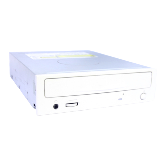
Page 6: Location Of Customer Controls
LOCATION OF CUSTOMER CONTROLS Front Panel Emergency Eject Hole Disc Tray Stop/Eject Button Volume Control Drive Activity Indicators Headphone Jack 1. Disc tray 4. Volume control This is the tray for the disc. Place the disc on the This is used to adjust the output volume of the ejected disc tray, then lightly push the tray (or headphone jack. - Page 7 Rear Panel IDE Interface Connector Analog Audio Output Connector Jumper Connector Power Connector Digital Audio Output Connector 1. Power Connector 3. Jumper Connector Connects to the power supply (5-and 12-V DC) of This jumper determines whether the drive is the host computer. configured as a master or slave.
-
Page 8: Disassembly
DISASSEMBLY 1. CABINET and CIRCUIT BOARD 1-3. Cabinet and Main Circuit Board A. Remove the Cabinet in the direction of arrow (4). DISASSEMBLY (See Fig. 1-3) 1-1. Bottom Chassis B. Release 2 hooks (a) and remove the CD Tray A. Release 4 screws (A) and remove the Bottom Chassis drawing forward. -
Page 9: Pick-Up
2-2. Pick-up A. Release 1 screw (C) and remove the Pick-up. Pick-up Unit Pick-up Fig. 2-2... -
Page 10: Glossary
GLOSSARY ATIP Absolute Time in Pre-groove. With an additional modulation of the “Wobble”, the “Groove” contains a time code information. Wobble The pre-groove in the Disc is not a perfect spiral but is wobbled. With : – A typical amplitude of 30 nm –... -
Page 11: Exploded View
EXPLODED VIEW PBM00 (MAIN C.B.A) -
Page 12: The Differences Of Cd-R/Cd-Rw Discs And General Cd-Rom
The differences of CD-R/CD-RW discs and General CD-ROM 1. Recording Layer Recordable CD has a wobbled pre-groove on the surface of disc for laser beam to follow track. Track pitch(p) a=30nm Read-only Disc CD-ROM (READ-ONLY DISC) Radial Direction Radial Error Signal 0.4~0.5 um Groove Land... -
Page 13: Disc Materials
3. Disc Materials 1) CD-ROM disc • It is composed of Silver _ colored aluminum plate and Reflective layer. • Groove (Pit) of aluminum plate make a track. • Laser wavelength : 780 nm, Laser Power (Read): 0.5mW • Signal is detected by the difference of reflective beam intensity between “pit”... -
Page 14: Reading Process Of Optical Disc
3) CD-RW Disc Label Printing Protective Layer Dielectric Layer(TL) Recording Layer Dielectric Layer(UL) Substrate (Polycarbonate) Groove Laser Beam • It is composed of polycarbonate layer, alloy(silver, arsenic) layer, aluminum reflectivity layer, protective layer. • An crystalized alloy layer is transformed into noncrystalized by the laser heat. Therefore, writing and reading is enabled by the difference of reflectivity. -
Page 15: Writing Process Of Cd-R Disc
5. Writing Process of CD-R Disc Incident (Write) Laser Power (Read) (Read) Laser Spot a b c d e f Position (Time) Laser Below "ORP"– Mark Too Short Spot Reflected At Optimum Record Power ("ORP") Light Signal Above "ORP" – Mark Too Long Recorded Mark Time... -
Page 16: Organization Of The Pca, Pma And Lead-In Area
7. Organization of the PCA, PMA and Lead-in Area 1) Layout of CD-ROM disc Disc Center Diameter 120 mm Diameter 46 mm Diameter 15 mm Center hole Clamping and Label Area Information Area Read Only Disc Lead-in Area Program Area Lead-out Area 2) Layout of CD-R/RW disc Disc Center... -
Page 17: Function Of Pca And Pma Area
8. Function of PCA and PMA area 1) PCA (Power Calibration Area) • PCA area is used to determine the correct Laser Power for a disc. – Method 1 : PCA area is divided by a track. – Method 2 : The previous Calibration value is referred. –... -
Page 18: Writing Process Of Disc
2) ROPC (Running Optimum Power Control) • Variable primary factor of Optimum Power – Change of Power sensitivity on the Disc. (limited to 0.05 *Po) – Wavelength shift of the laser diode due to the operating temperature change. – Change of the Spot aberration due to the Disc skew, Substrate thickness, Defocus. -
Page 19: Super Link
11. Super Link Super(SUPpressed Error Recording) link method is a new technology to link the interrupted recording by buffer under run. When drive¡fl s buffer will be under, the drive will stop recording and store the stop position. When drive¡fl s buffer receive data from HOST again, the drive will seek to the stop position of last recording and continue writing. -
Page 20: Dvd & Cd Data Processing
DVD & CD DATA PROCESSING 1. Data Processing Flow... -
Page 21: Copy Protection And Regional Code Management Block
2. Copy Protection and Regional Code Management Block Block Diagram Change the "KEY" HOST DVD PLAYER MT1628E (MPEG2 B/D) Scrambled MPEG Data KEY Management Control Brief Process 1. Regional Code for DVD Disc – DVD-ROM drive transfers the regional code of the control data to host by the command of host, the DVD player of host reads the regional code, and plays title in the case of allowed regional code only. -
Page 22: About Prevention The Dvd-Rom From To Be Copy
3. About Prevention the DVD-ROM from to be copy A data is able to encode and record in the disc, if a copyright holder wants to prevent the disc from copying. In case of a disc enhanced movie of 3 titles..DISC KEY (2048 Bytes) is used to encode the whole contents in the disc and TITLE KEY (5 Bytes) is used to encode the title respectively. -
Page 23: About The Dvd-Rom Regional Code
4. About the DVD-ROM Regional Code Regional code U.S.A PRI. VIR DISC ROM - DRIVE MPEG-2 BOARD VGA CARD MONITOR Transfer to Receiving If the board is setting to the regional The disc has MPEG-2 board data from the code 1 for the U.S.A..the regional reading the MPEG-2... -
Page 24: Internal Structure Of The Pick
INTERNAL STRUCTURE OF THE PICK-UP 1. Block Diagram of the PICK-UP... -
Page 25: Pick Up Pin Assignment
2. Pick up Pin Assignment Signal Name Signal Description Vc(OEIC) reference voltage input for OEIC (+2.3V) gain swich for signal OEIC output (Gain 8.7dB) signal OEIC output EF3 signal OEIC output D signal OEIC output C signal OEIC output EF4 signal OEIC output EF1 signal OEIC output A signal OEIC output B... -
Page 26: Signal Detection Of The P/U
3. Signal detection of the P/U Infrared Iaser Pick-Up module Focusing Tracking Photo Diode 1) Focus Error Signal ==> (A+C)-(B+D) This signal is generated in RF IC (IC200 : MT1616E) and controls the pick-up’s up and down to focus on Disc. -
Page 27: Description Of Circuit
DESCRIPTION OF CIRCUIT 1. ALPC (Automatic Laser Power Control) Circuit 1-1. Block Diagram IC 200 ( MT1616E) IC200 (MT1616E) RLDON CN 101 RFPDSH IC 100 VRDCO S/H & VRDC VRDC VRDCG & Level Shift & Gain Optical Pick-up RDAC MT1618E HOP-7041T MT1628E RREF... -
Page 28: Focus/Tracking/Sled Servo Circuit
2. Focus/Tracking/Sled Servo Circuit 2-1. Focus, Tracking & Sled Servo Process Focus, Tracking Servo IC200 MT1616E Pick - up Focus Erro r Detector A,B,C,D A,B,C,D,E, F,G,H Track Error Detector A,B,C,D E,F,G,H Tracking F ocusing Actuator IC100 Servo Control MT1618E MT1628E Focus x5 FOSO PARALLEL... -
Page 29: Spindle Servo Circuit
3. Spindle Servo Circuit 3-1. Spindle Servo Process IC200 MT1616E Pick- up WOBSI Wobble Signal Generator IC301 HD153704 Spindle Motor MT1628E IC100 MT1618E Hall Sensor IC300 M63028FP CD-DSP/SERVO CD WOBBLE CLV FG CAV 40X Decode PLL DMSO Frequency Controller LOCK FILTER DEFS MOTOR SPEE D... -
Page 30: Major Ic Internal Block Diagram And Pin Description
MAJOR IC INTERNAL BLOCK DIAGRAM AND PIN DESCRIPTION IC200 (MT1616E) : RF AMP Pin Assignment ATFG OSCL1CP GIO2 OSCL1CN EEP_CS RFAGCI EEP_SCLK RFAGCU EEP_SDATA RFAGC DRVOUT0 EQBIAS DRVOUT1 AVSS4 DRVOUT2 RFON RFOP LIMIT# AVDD4 LED2 RFIN LED1 RFIP TRAYIN# AVDD7 TRAYOUT# DVDA ENBL... - Page 31 Block Diagram AVSS7 VWDC2O AVDD7 Voltage VWDC1O AVSS6 ATIP/ Ref & DAC AVDD6 VRDCO Wobble AVSS5 VRDCN MPX2B AVDD5 MPX2 VRDC AVSS4 MPX1 AVDD4 MPX2B VRDCO VWDC1N WRFSH AVSS3 VWDC1O VWDC1 10-Bit VWDC2O AVDD3 R R E F FPDOLP AVSS2 WREF1 AVDD2 FPDO...
- Page 32 • Pin Description Symbol Type Description Numbers RF Signals & S/H Control Pulses HAVC Analog Output Decoupling Pin for Reference Voltage of Main and Sub Beams Analog Input Input of Main Beam Signal (A) Analog Input Input of Main Beam Signal (B) Analog Input Input of Main Beam Signal (C) Analog Input...
- Page 33 Symbol Type Description Numbers Digital Output (TTL), (1). High Speed Track Counting Digital Output HTRC/PHTO 4 mA Driving (2). Output of Photo Interrupt Signal EQRF Circuits EQBIAS Analog Output External Bias Connection for Circuits in EQRF Block External Capacitor Connection of Offset Ca ncellation Loop1 for OSCL1CP Analog Output VGA in EQRF Block (Positive)
- Page 34 Symbol Type Description Numbers VWDC1 Analog Output Midcourse Output of Laser Diode Control in CD -R/RW Write A PC VWDC1O Analog Output Output Voltage 1 of Laser Diode Control in CD-R/RW Write APC VWDC2O Analog Output Output Voltage 2 of Laser Diode Control in CD-R/RW Write APC DVDMDI Analog Input Laser Power Monitor Input for DVD APC...
- Page 35 Symbol Type Description Numbers Digital Output (TTL), EEP_CS EEPROM Chip Select Output. 4 mA Driving Digital Output (TTL), EEP_SCLK EEPROM Transmit Clock Output. 4 mA Driving Digital I/O (TTL), EEP_SDATA EEPROM Transmit Data Input/Output. 50K Pull-Down, 4mA Driving Digital Output (TTL), ENBL Laser Diode Enable Signal Output.
- Page 36 IC100 (MT1628E) : Encoder, Decoder & DSP Signal Processor Pin Diagram IREF IPLLVSS PLLVSS LPIOP LPIOP HD10 LPFON LPFIP DVDD33(4) LPFIN HD11 LPFOP JITFO DVSS JITFN HD12 PLLVDD33 HD13 FMO2 HD14 PWMOUT DVDD25 HD15 DMARQ DIOW# TRAYPWM DIOR# IORDY DVSS DVDD33 EJECT# DMACK#...
- Page 37 Functional Block Diagram TEST Wobble EFMPLL Data Wobble Signal Reset (efmclk Spindle Slicer Interface Logic PRST# Write Strategy logic synthesizer) Control Interface Logic PLLVDD33 IREF LPFIN LPFIP EFM/EFM+ Sync. FM Demodulator PLLVSS Data Demodulator XTALO Protection System JITFN & Bi-Phase data Subcode/ID Clock Demodulator...
- Page 38 Pin description Pin Numbers Symbol Type Description Data PLL Interface (11) PLLVDD33 Power Power for data PLL and related analog circuitry. JITFN Analog Input The input terminal of RF jitter meter. JITFO Analog Output The output terminal of RF jitter meter. LPFOP Analog Output The positive output of loop filter amplifier.
- Page 39 WFPDSH Sample pulse control signal for RF write APC. 3.3V LVTTL output, Default : 8mA Slew rate, 2mA, 4mA, 6mA, 8mA, 10mA, 12mA, 14mA, 16mA PDR RFPDSH Sample pulse control signal for RF read APC. 3.3V LVTTL output, Default : 4mA 2mA, 4mA, 6mA, 8mA, 10mA, 12mA, 14mA, 16mA PDR...
- Page 40 PWMOUT Analog Output General PWM output. DVDD33 Power (3.3V) Digital power in analog block. DVDD25 Power (2.5V) Digital power in analog block. DVSS Ground Digital power in analog block. Panel (2) EJECT# 3.3V LVTTL I/O, Eject/stop key input, active low. Alternate function : Internal monitored signal output.
- Page 41 UP3_1/UTXD 3.3V LVTTL I/O, Programmable bi-directional I/O. Slew rate, SMT, 4mA Alternate function : TXD. Turbo 8032 serial transmit data. driving, 75K pull-up PC RS232 serial transmit data. UP3_0/URXD 3.3V LVTTL I/O, Programmable bi-directional I/O. Slew rate, SMT, 4mA Alternate function : RXD. Turbo 8032 serial receive data. driving, 75K pull-up PC RS232 serial receive data.
- Page 42 EFMPLL VCO (4) EFMPLLVDD33 Analog power(3.3V) Power supply for EFMPLL circuitry. EFMVCOCIN Analog input EFMPLL VCO input. For external loop filter connection. EFMPLLVSS Ground Ground pin for EFMPLL circuitry. EFMLPFGND Analog input EFMPLL LPF ground input. Crystal Interface (2) XTALI Input X’tal input.
- Page 43 DQML 3.3V LVTTL output, SDRAM low-byte data output mask control signal, high active. PSR, For SDRAM application only. 2mA, 4mA, 6mA, Default : 4mA, slew rate 8mA, 10mA, 12mA, 14mA, 16mA PDR CASH#/ Column Address Strobe High/RAM Write Enable High. When a 3.3V LVTTL Output, RWEH# PSR,...
- Page 44 HRST# Host reset input. The active-low input is referred to as hardware 3.3V LVTTL Input, reset and is used to reset this chip. SMT,75K pull-up 147, 149, 151, HD15~HD0 Host Data bus. This is the 8-bit or 16-bit bi-directioinal data bus to 3.3V LVTTL I/O 153, 156, 159, the host.
- Page 45 PDIAG# Passed Diagnostics. This signal is asserted by Device 1 to 3.3V LVTTL I/O, indicate to Device 0 that it has completed diagnostics. Slew rate, 10mA driving, SMT, 40K pull-up 132,137,134 HA2,HA1,HA0 Device Address Bus. This is the 3-bit binary coded address 3.3V LVTTL Input, provided by the host to access an ATA register or data.
- Page 46 Digital Power Pins (26) 48, 95, 157 DVDD33(4) Power (3.3V) VDD for Input pad. 37, 83, 136, 186 DVDD25 Power (2.5V) VDD for internal circuit. 27, 58, 80, 111, DVDD33 Power(3.3V) VDD for output pad. 142, 165, 189 31, 61, 89, 105, DVSS Ground VSS for IO pad.
- Page 47 IC300 (M63028FP) : SPINDLE MOTOR AND 5CH ACTUATOR DRIVER Block Diagram FG X3 Reverse Detect Logic Logic MATRIX Hall Bias Current Current Current comp. amp. amp. comp. comp. amp. Direction Direction BIAS Direction SPIN comp. comp. Brake select comp. Frequency generator SL1IN SL2IN...
-
Page 48: Troubleshooting Guide
TROUBLESHOOTING GUIDE Reset or Power Check. Check it after connecting the power cable only on interface cable for NO Reset or Power ON. Are the pin 41 • Check the power(12V, 5V) short. and 44 of CN100 +12V and +5V •... - Page 49 System Check. Load tray without inserting disc. Does Tray operate normally? Go to “Tray operating is abnormal” Go to “Sled operating is abnormal” Does Pick-up move to inside? Does Pickup Go to “Focus Actuator operating is lens move up/down? abnormal”. Go to “Laser operating is abnormal”.
- Page 50 Tray operating is abnormal. Tray open/close doesn’t work. Is the input voltage • Check the connection of IC200 pin77. 0V at IC200 pin 77 when push the • Replace the SW801(/EJECT). SW801? • Check the connection of IC100 pin 19. Is there Tray •...
- Page 51 Sled operating is abnormal. Is there Sled control signal output? Replace the IC200. (IC100 pin 14,18) Is there • Check the connction of IC300 pin 1,2. Sled drive voltage input? • Replace the IC300. (IC300 pin 1,2) • Check the R305, R306. Is there Check the connection of IC200 Is MUTE1 signal ‘H’?
- Page 52 Spindle operating is abnormal Is there • Check the connection of IC100 pin Spindle control signal input? (IC300 pin 26) • Replace the IC100. Is there Is there • Check the connection of IC300 pin 24. Spindle drive voltage output? FG signal input? •...
- Page 53 Focus Servo is unstable Is FE signal output normal in Focusing Replace the IC200 Up/Down? (IC200 pin123) Is FOSO signal output normal in Focusing Replace the IC100. Up/Down? (IC100 pin 12) Go to “Focus Actuator operating is abnormal” Focus Actuator operating is abnormal •...
- Page 54 Recognition Fail Case 1: CD-ROM Fail Check Pickup Read Power Go to “LD CHECK”. was 0.8 ~1.3mW? Does Focus Servo Go to “Focus Servo is unstable”. operate normally? Check Pickup Check the Pick-up FFC and CN101. RF signal (RFO+) was Replace the Pick-up unit.
- Page 55 Recognition Fail Case 3 : DVD Disc Is IC200 Pin 100 level was Is Pickup Pin 15 (LD) level Replace the IC200. about 2.3V? about 3.7V? Replace the Q601. Replace the Pickup. Is there RF signal at CN101 Pin11? Is there RF signal at IC200 Pin30(RFOP) Replace the IC200.
- Page 56 Track Servo is unstable Is TE signal Is PICK UP • Check the PICK UP FFC. output normal in Focusing (E, F, G, H) output normal? • Replace the PICK UP. ON and Tracking OFF? (CN101 pin 3, 6, 7, 10) (IC200 pin 121) Replace the IC200.
- Page 57 Laser operating is abnormal Execute ‘B.Check ALPC Parameters’ of ‘How to use Test Tool’ Is EEPROM Data valid? Execute ‘D.Laser Inspection’ of Execute ‘C.Laser Power Setup’ of ‘How to use Test Tool’ ‘How to use Test Tool’ At ‘Test CD Read Power’ At ‘Test CD Write power’...
- Page 58 LD CHECK (Not Read) Execute ‘D. Laser inspection’ of ‘How to use Test Tool : [Test CD Read Power] Measured Power : Normal 800-1300µW? • Check the connection of IC200 Pin 26. CN101 Pin30(ENBL) = “H”? • Check and replace the IC200(RF). •...
- Page 59 LD CHECK (Not Recorded) Execute ‘D. Laser Inspection’ of ‘How to use Test Tool’ :[Test CD Write Power] Measured Power : Normal 28 ~ 32mW? • CN101 Pin 30 Check the connection of IC200 pin 26 • (ENBL) = ‘H’? Check and replace the IC200(RF) •...
- Page 60 Remove the Dust, Fingerprint and Does the disc if the disc has long width have any Dust, Scratch, Scratch, change it. Fingerprint...? Use LG bundle Software Is the write (Write Tool & Version) Tool(version) supported by - Easy CD Creator ... LG CD-RW/DVD-ROM Direct CD ...
- Page 61 Writing Part Check. Refer “Laser is abnormal”. Load tray with CD-R/RW Disc. Run the Writing Tool (Easy CD Creator or Nero). Run the Writing with Tool (Easy CD Creator or Nero). Does the Do the IC200(RF) blink of LED 801 occurs during pin 75 output toggle signals Writing? during Writing?
- Page 62 No audio output Insert the audio Disc. AUD_MUTE : ‘L’? • Check and replace the IC200. (IC200 Pin 70) Audio Play : AUD_MUTE ‘H’. Do LOUT, ROUT signals output? • Check and replace the IC100. (IC100 Pin 124, 126) Do audio Line signals output? (JK801 and CN100 •...
- Page 63 • How to use Test Tool A. Start 1. Install GCC-4480B –> PC Power ON –> Execute Windows. 2. Execute JcX.exe on Windows. 3. At Current Devices : you must select device you want to test. (Note: All device is displayed, so you identify the proper device by model name : GCC-4480B.)
- Page 64 C. Laser Power Setup (CD Read DAC/VWDC1/VWDC2/DVD Read DAC re-setup) 1. Remove disc on the tray. 2. Click “CD” button on the menu. 3. Measure LD Power with LD Powermeter. Type the result in the displyed message box. (Caution : wavelength = 780nm) 4.
- Page 65 D. Laser Inspection (CD Read power / Write power / DVD Read power) 1. Remove disc on the Tray. ========= Test CD Read Power =========== 2. Click “CD Read LD ON” button. 3. Measure LD Power with LD Powermeter(Caution : wavelength = 780nm) 4.
-
Page 66: Block Diagram
BLOCK DIAGRAM Optical 33.868MHz IC 200 Pick-up ABCD Serial HOP-7061T EFGH Commumication MT1616 RF Amp IC 100 Wobble Servo S/H, ALPC Spindle STEP VWDC Write S/H Signal General MT1628 Motor Motor VRDC port use EEPROM access EQRF, SBAD Decoder FEI, TEI, CSI, Encoder Writing cable...