Table of Contents
Advertisement
Quick Links
Advertisement
Table of Contents

Related Manuals for Asus AAEON PICO-APL1


Summary of Contents for Asus AAEON PICO-APL1
- Page 1 PICO-APL1 PICO-ITX Board User’s Manual 9 Last Updated: December 2, 2020...
- Page 2 Copyright Notice This document is copyrighted, 2020. All rights are reserved. The original manufacturer reserves the right to make improvements to the products described in this manual at any time without notice. No part of this manual may be reproduced, copied, translated, or transmitted in any form or by any means without the prior written permission of the original manufacturer.
- Page 3 Acknowledgement All other products’ name or trademarks are properties of their respective owners. Microsoft Windows® is a registered trademark of Microsoft Corp. ⚫ ITE is a trademark of Integrated Technology Express, Inc. ⚫ IBM, PC/AT, PS/2, and VGA are trademarks of International Business Machines ⚫...
- Page 4 Packing List Before setting up your product, please make sure the following items have been shipped: Item Quantity PICO-APL1 ⚫ COM + Line-out Cable (optional) ⚫ If any of these items are missing or damaged, please contact your distributor or sales representative immediately.
- Page 5 About this Document This User’s Manual contains all the essential information, such as detailed descriptions and explanations on the product’s hardware and software features (if any), its specifications, dimensions, jumper/connector settings/definitions, and driver installation instructions (if any), to facilitate users in setting up their product. Users may refer to the product page at AAEON.com for the latest version of this document.
- Page 6 Safety Precautions Please read the following safety instructions carefully. It is advised that you keep this manual for future references All cautions and warnings on the device should be noted. Make sure the power source matches the power rating of the device. Position the power cord so that people cannot step on it.
- Page 7 If any of the following situations arises, please the contact our service personnel: Damaged power cord or plug Liquid intrusion to the device iii. Exposure to moisture Device is not working as expected or in a manner as described in this manual The device is dropped or damaged Any obvious signs of damage displayed on the device...
- Page 8 FCC Statement This device complies with Part 15 FCC Rules. Operation is subject to the following two conditions: (1) this device may not cause harmful interference, and (2) this device must accept any interference received including interference that may cause undesired operation.
- Page 9 China RoHS Requirements (CN) 产品中有毒有害物质或元素名称及含量 AAEON Main Board/ Daughter Board/ Backplane 有毒有害物质或元素 部件名称 铅 汞 镉 六价铬 多溴联苯 多溴二苯醚 (Pb) (Hg) (Cd) (Cr(VI)) (PBB) (PBDE) 印刷电路板 ○ ○ ○ ○ ○ ○ 及其电子组件 外部信号 ○ ○ ○ ○ ○ ○ 连接器及线材...
- Page 10 China RoHS Requirement (EN) Poisonous or Hazardous Substances or Elements in Products AAEON Main Board/ Daughter Board/ Backplane Poisonous or Hazardous Substances or Elements Hexavalent Polybrominated Polybrominated Component Lead Mercury Cadmium Chromium Biphenyls Diphenyl Ethers (Pb) (Hg) (Cd) (Cr(VI)) (PBB) (PBDE) PCB &...
-
Page 11: Table Of Contents
Table of Contents Chapter 1 - Product Specifications..................1 Specifications ......................2 Chapter 2 – Hardware Information ..................5 Dimensions ....................... 6 Jumpers and Connectors ..................9 List of Jumpers ......................11 2.3.1 Clear CMOS Jumper (JP1 1, 3, 5) .............. 12 2.3.2 Auto Power Button Enable/Disable Selection (JP1 2, 4, 6) .... - Page 12 2.4.15 LVDS Port (CN16) ..................27 2.4.16 COM Port 1/2 & line out connector (CN17) ......... 29 2.4.17 COM Port2 RS-485 ..................30 2.4.18 COM Port2 RS-422 ..................30 2.4.19 LPC Port (CN18)................... 31 2.4.20 USB 2.0 Port 1 (CN19) ................32 Specifications for I/O Port..................
- Page 13 Boot .......................... 59 3.7.1 BBS Priorities ....................60 Save & Exit ....................... 61 Chapter 4 – Drivers Installation .................... 62 Driver Download/Installation ................63 Appendix A - I/O Information ....................65 I/O Address Map ....................66 Memory Address Map ..................67 IRQ Mapping Chart ....................
-
Page 14: Chapter 1 - Product Specifications
Chapter 1 Chapter 1 - Product Specifications... -
Page 15: Specifications
Specifications System Pico-ITX Form Factor Intel Atom E3900 series Intel Pentium N4200 Intel Celeron N3350 Processor SoC Up to 2.0GHz CPU Frequency Intel Atom E3900 series Chipset Intel Pentium N4200 Intel Celeron N3350 Processor SoC 204-pin DDR3L SODIMM x 1, DDR3L 1867MHz Memory Type Max. - Page 16 System 32 °F~ 140 °F (0°C ~ 60°C), Operating Temperature -40 °F ~ 176 °F (-40°C ~ 80°C) Storage Temperature 0% ~ 90% relative humidity, non-condensing Operating Humidity 170,000 MTBF (Hours) CE, FCC Certification Display Intel Atom E3900 series Chipset Intel Pentium N4200 Intel Celeron N3350 Processor SoC LVDS (18/24bit 2CH) 1920 x 1200 (optional)
- Page 17 4-bit (2-in, 2-out) Mini Card (Half-size) x 1 Expansion Slot BIO (optional) x 1 I2C or SMBus x 1 — — — Touch Chapter 1 – Product Specifications...
-
Page 18: Chapter 2 - Hardware Information
Chapter 2 Chapter 2 – Hardware Information... -
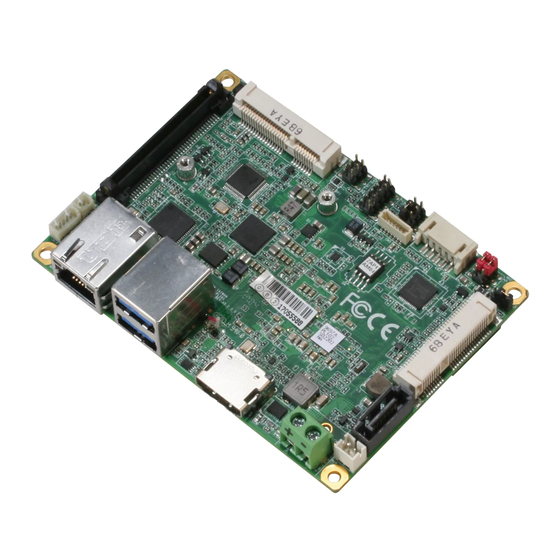
Page 19: Dimensions
Dimensions Component Side Component Side MATER >0 ¡ Ó 0 .1 SPEC.: >10 ¡ Ó 0 .2 >50 ¡ Ó 0 .3 FINISH: >200 ¡ Ó 0 .5 >500 ¡ Ó 0 .8 UNIT: M ANGLE TOL. SCALE: ¡ Ó 0 .5¢X Chapter 2 –... - Page 20 ITEM DATE REMARK Solder Side Solder Side 1907APL102 MATERIAL: PART No. >0 ¡ Ó 0 .1 t=1.6mm 1907APL102 SPEC.: DWG No. >10 ¡ Ó 0 .2 >50 ¡ Ó 0 .3 NAME PCB drawing FINISH: APPROVED CHECKED DESIGNED >200 ¡ Ó 0 .5 >500 ¡...
- Page 21 Rear I/O Configuration Chapter 2 – Hardware Information...
-
Page 22: Jumpers And Connectors
Jumpers and Connectors Component Side Component Side MATERI >0 ¡ Ó 0 .1 SPEC.: >10 ¡ Ó 0 .2 >50 ¡ Ó 0 .3 FINISH: >200 ¡ Ó 0 .5 >500 ¡ Ó 0 .8 UNIT: M ANGLE TOL. SCALE: ¡... - Page 23 ITEM DATE REMARK Solder Side Solder Side 1907APL102 MATERIAL: PART No. >0 ¡ Ó 0 .1 t=1.6mm SPEC.: DWG No. 1907APL102 >10 ¡ Ó 0 .2 >50 ¡ Ó 0 .3 PCB drawing FINISH: APPROVED CHECKED DESIGNED NAME >200 ¡ Ó 0 .5 >500 ¡...
-
Page 24: List Of Jumpers
List of Jumpers Please refer to the table below for all of the board’s jumpers that you can configure for your application Label Function JP1(1,3,5) Clear CMOS Jumper JP1(2,4,6) Auto Power Button Enable/Disable Selection JP2(1,3,5) LVDS Port Operating Voltage Selection JP2(2,4,6) LVDS Port Backlight Inverter Voltage Selection LVDS Port Backlight Lightness Control Mode Selection... -
Page 25: Clear Cmos Jumper (Jp1 1, 3, 5)
2.3.1 Clear CMOS Jumper (JP1 1, 3, 5) Normal (Default) Clear CMOS 2.3.2 Auto Power Button Enable/Disable Selection (JP1 2, 4, 6) Enable (Default) Disable 2.3.3 LVDS Port Operating Voltage Selection (JP2 1,3,5) +3.3V (Default) 2.3.4 LVDS Port Backlight Inverter Voltage Selection (JP2 2,4,6) +12V +5V (Default) Chapter 2 –... -
Page 26: Lvds Port Backlight Lightness Control Mode (Jp3)
2.3.5 LVDS Port Backlight Lightness Control Mode (JP3) VR Mode (Default) PWM Mode Chapter 2 – Hardware Information... -
Page 27: List Of Connectors
List of Connectors Please refer to the table below for all of the board’s connectors that you can configure for your application Label Function Digital IO Port LVDS Port Inverter / Backlight Connector Front Panel Mini-Card Slot (Half-Mini Card) SPI Programming Header Mini-Card Slot (Full-Mini Card)/mSATA (By BOM) BIO connector SATA Port... -
Page 28: Digital Io Port (Cn1)
2.4.1 Digital IO Port (CN1) Pin Name Signal Type Pin Name DIO0 DIO1 DIO2 DIO3 2.4.2 LVDS Port Inverter / Backlight Connector (CN2) Pin Name Signal Type Signal level BKL_PWR +5V / +12V BKL_CONTROL BKL_ENABLE +3.3V Note1: LVDS/BKL_PWR can be set to +5V or +12V by JP2. Chapter 2 –... -
Page 29: Front Panel (Cn3)
Note2: LVDS/BKL_CONTROL can be set by JP3. Note3: The driving current supports up to 2A. 2.4.3 Front Panel (CN3) Pin Name Pin Name PWR_BTN- PWR_BTN+ HDD_LED- HDD_LED+ SPEAKER- SPEAKER+ PWR_LED- PWR_LED+ H/W RESET- H/W RESET+ 2.4.4 Mini-Card Slot (Half-Mini Card) (CN4) Pin Name Signal Type Signal Level... - Page 30 Pin Name Signal Type Signal Level PCIE_REF_CLK- DIFF PCIE_REF_CLK+ DIFF W_DISABLE# +3.3V PCIE_RST# +3.3V PCIE_RX- DIFF +3.3VSB +3.3V PCIE_RX+ DIFF +1.5V +1.5V SMB_CLK +3.3V PCIE_TX- DIFF SMB_DATA +3.3V PCIE_TX+ DIFF Chapter 2 – Hardware Information...
- Page 31 Pin Name Signal Type Signal Level USB_D- DIFF USB_D+ DIFF +3.3VSB +3.3V +3.3VSB +3.3V +1.5V +1.5V +3.3VSB +3.3V Chapter 2 – Hardware Information...
-
Page 32: Mini-Card Slot (Full Mini-Card)/Msata (By Bom) (Cn6)
2.4.5 Mini-Card Slot (Full Mini-Card)/mSATA (by BOM) (CN6) Pin Name Signal Type Signal Level PCIE_WAKE# +3.3VSB/+3.3V +3.3V +1.5V +1.5V PCIE_CLK_REQ# UIM_PWR UIM_DATA PCIE_REF_CLK- DIFF UIM_CLK PCIE_REF_CLK+ DIFF UIM_RST UIM_VPP W_DISABLE# +3.3V PCIE_RST# +3.3V PCIE_RX-/mSATARX+ DIFF +3.3VSB/+3.3V +3.3V Chapter 2 – Hardware Information... - Page 33 Pin Name Signal Type Signal Level PCIE_RX+/mSATARX- DIFF +1.5V +1.5V SMB_CLK +3.3V PCIE_TX-/mSATATX- DIFF SMB_DATA +3.3V PCIE_TX+/mSATATX+ DIFF USB_D- DIFF USB_D+ DIFF +3.3VSB/+3.3V +3.3V +3.3VSB/+3.3V +3.3V +1.5V +1.5V Chapter 2 – Hardware Information...
-
Page 34: Bio Connector (Cn7)
Pin Name Signal Type Signal Level +3.3VSB/+3.3V +3.3V 2.4.6 BIO connector (CN7) Pin Name Pin Name +12VSB PCIE_TXN0 PCIE_RXN0 PCIE_TXP0 PCIE_RXP0 PCIE_TXN4 PCIE_RXN4 PCIE_TXP4 PCIE_RXP4 PS_ON# DDI0_DDCCLK_3P3 DDI0_DDCDATA_3P3 +5VSB +5VSB +5VSB +5VSB PCIE_REF_CLK0 RESET# PCIE_REF_CLK0# DDI0_TXN1 DDI0_TXN0 DDI0_TXP1 DDI0_TXP0 DDI0_TXN3 DDI0_TXN2 DDI0_TXP3 DDI0_TXP2... - Page 35 Pin Name Pin Name DDI0_AUXN DDI0_ AUXP USB3_TX2_N USB3_TX2_P USBN4 USBP4 USB3_RX2_N USB3_RX2_P SMB_CLK SMB_DATA WAKE# USB_OC0# USB_OC1# LPC_AD0 LPC_FRAME# LPC_AD1 SERIRQ LPC_AD2 LPC_DRQ LPC_AD3 GPIO0/BIO-POWEROK AGND LPC_CLK AUD_LINEOUT_L PME# AUD_LINEOUT_R Chapter 2 – Hardware Information...
-
Page 36: Sata Port (Cn8)
2.4.7 SATA Port (CN8) Pin Name Signal Type Signal Level SATA_TX1+ DIFF SATA_TX1- DIFF SATA_RX1- DIFF SATA_RX1+ DIFF 2.4.8 Battery (CN9) Pin Name Signal Type Signal Level +3.3V 3.3V Chapter 2 – Hardware Information... -
Page 37: Lan (Rj-45) Port (Cn10)
2.4.9 LAN (RJ-45) Port (CN10) Pin Name Signal Type Signal Level MDI0+ DIFF MDI0- DIFF MDI1+ DIFF MDI2+ DIFF MDI2- DIFF MDI1- DIFF MDI3+ DIFF MDI3- DIFF 2.4.10 USB3.0 Ports 0 and 1 (CN11) Pin Name Signal Type Signal Level +5VSB USB0_D- DIFF... -
Page 38: Output For Sata Hdd (Cn12)
Pin Name Signal Type Signal Level USB0_SSTX− DIFF USB0_SSTX+ DIFF +5VSB USB1_D- DIFF USB1_D+ DIFF USB1_SSRX− DIFF USB1_SSRX+ DIFF USB1_SSTX− DIFF USB1_SSTX+ DIFF 2.4.11 +5V Output for SATA HDD (CN12) Pin Name Signal Type Signal Level Chapter 2 – Hardware Information... -
Page 39: Hdmi Port (Cn13)
2.4.12 HDMI Port (CN13) Pin Name Signal Type Signal level TMDS_DAT2+ DIFF TMDS_DAT2- DIFF TMDS_DAT1+ DIFF TMDS_DAT1- DIFF TMDS_DAT0+ DIFF TMDS_DAT0- DIFF TMDS_CLK+ DIFF TMDS_CLK- DIFF DDC_CLK DDC_DATA HPLG_DETECT Chapter 2 – Hardware Information... -
Page 40: External +12V Input (Cn14)
2.4.13 External +12V Input (CN14) Pin Name Signal Type Signal Level +121V +12V 2.4.14 DDR3L SO-DIMM Slot (CN15) Standard specification 2.4.15 LVDS Port (CN16) Note1: LVDS LCD_PWR can be set to +3.3V or +5V by JP2 Note2: The max. driving current is 2A. Pin Name Signal Type Signal Level... - Page 41 Pin Name Signal Type Signal Level LVDS_DA0- DIFF LVDS_DA0+ DIFF LVDS_DA1- DIFF LVDS_DA1+ DIFF LVDS_DA2- DIFF LVDS_DA2+ DIFF LVDS_DA3- DIFF LVDS_DA3+ DIFF DDC_DATA +3.3V DDC_CLK +3.3V LVDS_DB0- DIFF LVDS_DB0+ DIFF LVDS_DB1- DIFF LVDS_DB1+ DIFF LVDS_DB2- DIFF LVDS_DB2+ DIFF LVDS_DB3- DIFF LVDS_DB3+ DIFF LCD_PWR...
-
Page 42: Com Port 1/2 & Line Out Connector (Cn17)
2.4.16 COM Port 1/2 & line out connector (CN17) Pin Name Signal Type Signal Level DCDB DSRB RTSB ±9V ±9V CTSB DTRB ±9V RIB/+5V/+12V IN/ PWR +5V/+12V DCDA DSRA RTSA ±9V ±9V CTSA DTRA ±9V AGND LOUT_R LOUT_L Chapter 2 – Hardware Information... -
Page 43: Com Port2 Rs-485
2.4.17 COM Port2 RS-485 Pin Name Signal Type Signal Level RS485_D- ±5V RS485_D+ ±5V NC/+5V/+12V +5V/+12V 2.4.18 COM Port2 RS-422 Pin Name Signal Type Signal Level RS422_TX- ±5V RS422_TX+ ±5V RS422_RX+ RS422_RX- NC/+5V/+12V +5V/+12V Note1: COM2 RS-232/422/485 can be set by BIOS setting. Default is RS-232. Note2: COM2 RI/+5V/+12V function can be set by BOM (R248-RI/ R256-+12V/ R250-+5V) Chapter 2 –... -
Page 44: Lpc Port (Cn18)
2.4.19 LPC Port (CN18) Pin Name Signal Type Signal Level LAD0 +3.3V LAD1 +3.3V LAD2 +3.3V LAD3 +3.3V +3.3V +3.3V LFRAME# LRESET# +3.3V LCLK SMB_DATA [Default]/I2C_DATA +3.3V SMB_CLK [Default]/I2C_CLK +3.3V SMB_ALERT [Default]/INT_SERIRQ +3.3V Chapter 2 – Hardware Information... -
Page 45: Usb 2.0 Port 1 (Cn19)
2.4.20 USB 2.0 Port 1 (CN19) Pin Name Signal Type Signal Level +5VSB USBD5- DIFF USBD5+ DIFF Chapter 2 – Hardware Information... -
Page 46: Specifications For I/O Port
Specifications for I/O Port Reference Signal Name Rate Output Digital IO Port D0~D3 +5V/ (Open drain) LVDS Port Inverter/ +5V/2A or +12V/2A Backlight Connector +3.3VSB +3.3V/1.1A Mini-Card Slot +1.5V +1.5V/0.375A +3.3VSB +3.3V/1.1A Mini-Card Slot +1.5V +1.5V/0.375A USB 3.0 Port 1 & 2 CN10 +5VSB +5VSB/1A (per channel) -
Page 47: Function Block
Function Block Chapter 2 – Hardware Information... -
Page 48: Chapter 3 - Ami Bios Setup
Chapter 3 Chapter 3 - AMI BIOS Setup... -
Page 49: System Test And Initialization
System Test and Initialization The system uses certain routines to perform testing and initialization during the boot up sequence. If an error, fatal or non-fatal, is encountered, the system will output a few short beeps or display an error message. The system can usually continue the boot up sequence with non-fatal errors. -
Page 50: Ami Bios Setup
AMI BIOS Setup AMI BIOS ROM has a built-in Setup program that allows users to modify the basic system configuration. This type of information is stored in battery-backed CMOS RAM and BIOS NVRAM so that it retains the Setup information when the power is turned off. Entering Setup Power on the computer and press <Del>or <ESC>... -
Page 51: Main
Main Options Summary System Date Day MM:DD:YYYY Change the month, year and century. The ‘Day’ is changed automatically. System Time HH : MM : SS Change the clock of the system. Chapter 3 – AMI BIOS Setup... -
Page 52: Advanced
Advanced Options Summary CPU Configuration Menu for CPU Configuration Parameters SATA Configuration Menu for SATA Device Configuration Hardware Monitor Display system hardware status (CPU temperature, etc.) SIO Configuration SIO Chip configuration. Enable or Disable SIO Logical Devices, Resources and Features settings, etc. -
Page 53: Cpu Configuration
3.4.1 CPU Configuration Options Summary C-States Disabled Enabled Optimal Default, Failsafe Default Enable/Disable C States. EIST™ Disabled Enabled Optimal Default, Failsafe Default Enable/Disable Intel SpeedStep. Turbo Mode Disabled Enabled Optimal Default, Failsafe Default Turbo mode Intel Virtualization Disabled Technology Enabled Optimal Default, Failsafe Default When enabled, a VMM can utilize the additional hardware capabilities provided by Vanderpool Technology. - Page 54 Options Summary Power Limit 1 Enable Disabled Optimal Default, Failsafe Default Enabled Enable/Disable Power Limit 1 Chapter 3 – AMI BIOS Setup...
-
Page 55: Sata Configuration
3.4.2 SATA Configuration Options Summary SATA GEN SPEED AUTO Optimal Default, Failsafe Default GEN1 GEN2 GEN3 SATA GEN SPEED selection Port 0/ mSATA port Disabled Optimal Default, Failsafe Default Enabled Enable/ Disable SATA port Chapter 3 – AMI BIOS Setup... -
Page 56: Hardware Monitor
3.4.3 Hardware Monitor Chapter 3 – AMI BIOS Setup... -
Page 57: Sio Configuration
3.4.4 SIO Configuration Options Summary Serial Port 1/2 Configuration View and Set Basic properties of the SIO Logical device. Like IO Base , IRQ Range , DMA Channel and Device Mode. Chapter 3 – AMI BIOS Setup... -
Page 58: Serial Port Configuration
3.4.4.1 Serial Port Configuration Options Summary Use This Device Disable Enable Optimal Default, Failsafe Default Enable or Disable this Logical Device. Possible: Use Automatic Settings Optimal Default, Failsafe Default IO=2F8h; IRQ=3 IO=3F8h; IRQ=4 Allows user to change Device's Resource settings. New settings will be reflected on This Setup Page after System restarts. -
Page 59: Dio Configuration
3.4.5 DIO Configuration Options Summary DIO * Output Input Set DIO as Input or Output Level High Optimal Default, Failsafe Default Set output level when DIO pin is output Chapter 3 – AMI BIOS Setup... -
Page 60: Trusted Computing
3.4.6 Trusted Computing Options Summary Security Device Disable Support Enable Optimal Default, Failsafe Default Enables or Disables BIOS support for security device. O.S. will not show Security Device. TCG EFI protocol and INT1A interface will not be available. SHA-1 PCR Bank Disable Enable Optimal Default, Failsafe Default... - Page 61 Options Summary Platform Hierarchy Disabled Enabled Optimal Default, Failsafe Default Enable or disable Platform Hierarchy Storage Hierarchy Disabled Enabled Optimal Default, Failsafe Default Enable or Disable Storage Hierarchy Endorsement Disabled Hierarchy Enabled Optimal Default, Failsafe Default Enable or Disable Endorsement Hierarchy TPM2.0 UEFI Spec TCG_1_2 Version...
-
Page 62: Power Management
3.4.7 Power Management Options Summary Power Mode ATX Type Optimal Default, Failsafe Default AT Type Select system power mode Restore AC Power Loss Last State Optimal Default, Failsafe Default Always On Always Off Determine if the system turns on or off after AC resume from G3 to S5 state RTC wake system from Disable Optimal Default, Failsafe Default... -
Page 63: Chipset
Chipset Chapter 3 – AMI BIOS Setup... -
Page 64: North Bridge
3.5.1 North Bridge Chapter 3 – AMI BIOS Setup... -
Page 65: Lvds Panel Configuration
3.5.1.1 LVDS Panel Configuration Options Summary LVDS Disabled Enabled Optimal Default, Failsafe Default Enable/Disabled this panel. LVDS Panel Type 640X480@60HZ 800X480@60HZ 800X600@60HZ 1024X600@60HZ 1024X768@60HZ Optimal Default, Failsafe Default 1280X768@60HZ 1280X800@60HZ 1280X1024@60HZ 1366X768@60HZ 1440X900@60HZ 1600X1200@60HZ 1920X1080@60HZ 1920X1200@60HZ Chapter 3 – AMI BIOS Setup... - Page 66 Options Summary Select LCD panel used by Internal Graphics Device by selecting the appropriate setup item. Color Depth 18-bit Optimal Default, Failsafe Default 24-bit 36-bit 48-bit Select panel depth Backlight Type Normal Optimal Default, Failsafe Default Inverted Select backlight control signal type Backlight Level Optimal Default, Failsafe Default 100%...
-
Page 67: South Bridge
3.5.2 South Bridge Options Summary HD-Audio Support Disabled Enabled Optimal Default, Failsafe Default Enable/Disabled HD audio PCIe Speed Auto Optimal Default, Failsafe Default Gen1 Gen2 Configure PCIe Speed Chapter 3 – AMI BIOS Setup... -
Page 68: Security
Security Change User/Administrator Password You can set an Administrator Password or User Password. An Administrator Password must be set before you can set a User Password. The password will be required during boot up, or when the user enters the Setup utility. A User Password does not provide access to many of the features in the Setup utility. -
Page 69: Secure Boot
3.6.1 Secure Boot Options Summary Secure Boot Disabled Optimal Default, Failsafe Default Enabled Secure Boot feature is Active if Secure Boot is Enabled, Platform Key(PK) is enrolled and the System is in User mode. The mode change requires platform reset Secure Boot Mode Custom Optimal Default, Failsafe Default... -
Page 70: Key Management
3.6.1.1 Key Management Options Summary Factory Key Provision Disabled Optimal Default, Failsafe Default Enabled Secure Boot feature is Active if Secure Boot is Enabled, Platform Key(PK) is enrolled and the System is in User mode. The mode change requires platform reset Restore Factory Keys Force System to User Mode. - Page 71 Options Summary Remove 'UEFI CA' from Device Guard ready system must not list 'Microsoft UEFI CA' Certificate in Authorized Signature database (db) Restore DB defaults Restore DB variable to factory defaults Platform Key(PK) Details Export Update Delete Key Exchange Keys Details Export Update...
-
Page 72: Boot
Boot Options Summary Quiet Boot Disabled Enabled Optimal Default, Failsafe Default EnableDisable showing boot logo. Monitor Mwait Disable Enabled Auto Optimal Default, Failsafe Default Enable/Disable Monitor Mwait. To install Linux OS, please set this item to disable. Ipv4 PXE Support Disabled Optimal Default, Failsafe Default Enabled... -
Page 73: Bbs Priorities
3.7.1 BBS Priorities Chapter 3 – AMI BIOS Setup... -
Page 74: Save & Exit
Save & Exit Chapter 3 – AMI BIOS Setup... -
Page 75: Chapter 4 - Drivers Installation
Chapter 4 Chapter 4 – Drivers Installation... -
Page 76: Driver Download/Installation
Driver Download/Installation Drivers for the PICO-APL1 can be downloaded from the product page on the AAEON website by following this link: https://www.aaeon.com/en/p/pico-itx-boards-pico-apl1#downloads Download the driver(s) you need and follow the steps below to install them. Step 1 – Install Chipset Driver Open the STEP1 - CHIPSET folder and open the SetupChipset.exe file Follow the instructions Drivers will be installed automatically... - Page 77 Step 4 – Install Audio Driver Open the STEP4 - AUDIO folder and open the 0006-64bit_Win7_Win8_Win81_Win10_R279.exe file Follow the instructions Driver will be installed automatically Step 5 – Install TXE Driver Open the STEP5 - TXE folder and open the SetupTXE.exe file Follow the instructions Driver will be installed automatically Step 6 –...
-
Page 78: Appendix A - I/O Information
Appendix A Appendix A - I/O Information... -
Page 79: I/O Address Map
I/O Address Map Appendix A – I/O Information... -
Page 80: A.2 Memory Address Map
A.2 Memory Address Map Appendix A – I/O Information... -
Page 81: A.3 Irq Mapping Chart
A.3 IRQ Mapping Chart Appendix A – I/O Information... -
Page 82: Appendix B - Mating Connectors
Appendix B Appendix B – Mating Connectors... -
Page 83: List Of Mating Connectors And Cables
List of Mating Connectors and Cables The table notes mating connectors and available cables. Connector Function Mating Connector Available Cable P/N Label Cable Vendor Model no Digital IO Molex 51110-0650 Port LVDS Port PHR-5 Inverter / Backlight Connector Front Panel Molex 51110-1050 Front Panel... - Page 84 Connector Function Mating Connector Available Cable P/N Label Cable Vendor Model no CN19 Molex 51021-0500 USB Cable 1700050207 Connector Appendix B – Mating Connectors...
-
Page 85: Appendix C - Pico-Apl1-Semi Quick Installation Guide
Appendix C Appendix C – PICO-APL1-SEMI Quick Installation Guide... -
Page 86: Packing List
Packing List Before setting up your product, please make sure the following items have been shipped: Item Description Remark PICO-APL1 Chassis (Major parts) Bottom Cover of Chassis Accessory kits (w/ power button) QIG (This Document) A0.3 Appendix C – PICO-APL1-SEMI Quick Installation Guide... - Page 87 Appendix C – PICO-APL1-SEMI Quick Installation Guide...
-
Page 88: Assembly Procedure
Assembly procedure Step 1. Assemble the MB Insert memory into the socket at about 30 degrees. Push it down gently until secured. Remove the nut and shim ring from the DC-Jack on the MB. Appendix C – PICO-APL1-SEMI Quick Installation Guide... - Page 89 Gently insert the COM Port 1/2 & line out connector cable. It will “click” once in place. Make sure to orient the connector as in the picture below. Appendix C – PICO-APL1-SEMI Quick Installation Guide...
- Page 90 Step 2. Install MB into Chassis Remove the protective liner from thermal pad. Set MB onto chassis, being sure to line up the four holes with the posts. Fasten the MB to the chassis with four screws. Appendix C – PICO-APL1-SEMI Quick Installation Guide...
- Page 91 Fasten 2 screws on the side of the chassis for COM Port. Thread the power button cable from outside to inside of the chassis. Gently insert the button (it will ‘click’ when in place). Connect the power button cable to CN3 PIN1,2,3. Appendix C –...
- Page 92 Step 3. Finish System Assembly Fasten the nut and shim ring of DC-Jack on MB (be sure to put the shim ring on before the nut, as shown below). Stick the battery to the board. Slide the bottom cover onto the main chassis. Fasten the bottom cover to main chassis with four flat black screws;...
- Page 93 Appendix C – PICO-APL1-SEMI Quick Installation Guide...
-
Page 94: Appendix D - Pico-Apl1 Ai Core Kit Installation Guide
Appendix D Appendix D – PICO-APL1 AI Core Kit Installation Guide... -
Page 95: Product Brief
Product Brief The AAEON PICO-APL1 AI (artificial intelligence) Core product is bundled with the Intel Movidius Myriad 2 VPU. Before you start to set up the development environment, we suggest you prepare the following items: Up to 2G DRAM At least 4GB of free storage space connected to the CN8 or CN12 SATA... -
Page 96: Update Ubuntu And Kernel
Update Ubuntu and Kernel Step 1. To open terminal, select search Step 2. Type ‘cmd’ or ‘terminal’ Appendix D – PICO-APL1 AI Core Kit Installation Guide... - Page 97 Step 3. Type sudo apt update and press enter. Step 4. Type sudo apt full-upgrade -y Appendix D – PICO-APL1 AI Core Kit Installation Guide...
- Page 98 Step 5. After system finishes, type sudo reboot and the system will restart Step 6. After the restart, open terminal again. Appendix D – PICO-APL1 AI Core Kit Installation Guide...
-
Page 99: Install Ncsdk
Install NCSDK (Please refer to https://developer.movidius.com/start Step 1. In terminal, type mkdir -p ~/workspace Step 2. Type cd~/workspace Appendix D – PICO-APL1 AI Core Kit Installation Guide... - Page 100 Step 3. Type sudo apt install git Step 4. Type git clone https://github.com/movidius/ncsdk.git Appendix D – PICO-APL1 AI Core Kit Installation Guide...
- Page 101 Step 5. Type cd ~/workspace/ncsdk Step 6. Type make install Note: If the installation fails, run ‘make install’ again. Appendix D – PICO-APL1 AI Core Kit Installation Guide...
-
Page 102: Download Movidius Ncappzoo
Download Movidius Ncappzoo Step 1. In terminal, type cd ~/workspace Appendix D – PICO-APL1 AI Core Kit Installation Guide... - Page 103 Step 2. Type git clone https://github.com/movidius/ncappzoo Step 3. Type cd ~/workspace/ncappzo/apps/street_cam && make opencv Appendix D – PICO-APL1 AI Core Kit Installation Guide...
- Page 104 After installing NCSDK, Ncappzoo and OpenCV, you can start running demos. Step 1. Type cd ~/workspace/ncappzoo/apps Step 2. Type ls –I You will see the names of the folders in the directory. Appendix D – PICO-APL1 AI Core Kit Installation Guide...
- Page 105 Step 3. Type cd to open the folder you want. folder name Step 4. Type make help to view the commands you can use in each folder. Appendix D – PICO-APL1 AI Core Kit Installation Guide...
-
Page 106: Example In Movidius Ncappzoo
Example in Movidius Ncappzoo *(example: cd ~/workspace/ncappzoo/apps/hello_ncs_cpp && make run) Step 1. Type cd ~/workspace/ncappzoo/apps/hello_ncs_cpp Appendix D – PICO-APL1 AI Core Kit Installation Guide... - Page 107 Step 2. Type make help to view the commands you can use in the folder. Step 3. Type make run Appendix D – PICO-APL1 AI Core Kit Installation Guide...
-
Page 108: Additional Information
Additional Information With some relative directories, for example “video or graphic” relative directories, you need to install “opencv” before you can start working. You can install “opencv” with the following commands in terminal: cd~ workspace/ncappzo/apps/stree_cam make opencv. Other Some demos might need two or more Movidius modules, an Internet connection, or a USB Camera.