Table of Contents
Advertisement
R-N402/R-N402D
■ CONTENTS
TO SERVICE PERSONNEL ........................................... 2
FRONT PANELS ............................................................ 3
REAR PANELS .............................................................. 4
REMOTE CONTROL PANEL ......................................... 7
SPECIFICATIONS .......................................................... 7
INTERNAL VIEW ......................................................... 10
SERVICE PRECAUTIONS ........................................... 10
DISASSEMBLY PROCEDURES ...................................11
UPDATING FIRMWARE ............................................... 15
SELF-DIAGNOSTIC FUNCTION ................................. 18
1 0 1 3 7 2
NETWORK RECEIVER
SERVICE MANUAL
DISPLAY DATA ............................................................ 39
IC DATA ........................................................................ 43
BLOCK DIAGRAMS ..................................................... 47
WIRING DIAGRAM ...................................................... 49
PRINTED CIRCUIT BOARDS ...................................... 50
PIN CONNECTION DIAGRAMS .................................. 59
SCHEMATIC DIAGRAMS ............................................ 61
REPLACEMENT PARTS LIST ..................................... 69
REMOTE CONTROL .................................................... 82
'16.10
Advertisement
Table of Contents

Related Manuals for Yamaha R-N402


Summary of Contents for Yamaha R-N402
-
Page 1: Table Of Contents
NETWORK RECEIVER R-N402/R-N402D SERVICE MANUAL ■ CONTENTS TO SERVICE PERSONNEL ........... 2 DISPLAY DATA ............39 IC DATA ................ 43 FRONT PANELS ............3 BLOCK DIAGRAMS ............. 47 REAR PANELS .............. 4 WIRING DIAGRAM ............49 REMOTE CONTROL PANEL ......... 7 SPECIFICATIONS ............ -
Page 2: To Service Personnel
R-N402/R-N402D ■ TO SERVICE PERSONNEL AC LEAKAGE WALL EQUIPMENT TESTER OR 1. Critical Components Information OUTLET UNDER TEST EQUIVALENT Components having special characteristics are marked ⚠ and must be replaced with parts having specifications equal to those originally installed. 2. Leakage Current Measurement (For 120V Models Only) -
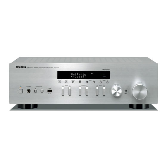
Page 3: Front Panels
R-N402/R-N402D ■ FRONT PANELS R-N402 R-N402D... -
Page 4: Rear Panels
R-N402/R-N402D ■ REAR PANELS R-N402 (U model) R-N402 (R model) R-N402 (T model) - Page 5 R-N402/R-N402D R-N402 (K model) R-N402 (A model) R-N402 (B, G models)
- Page 6 R-N402/R-N402D R-N402 (L model) R-N402 (S model) R-N402D (B, G models)
-
Page 7: Remote Control Panel
R-N402/R-N402D ■ REMOTE CONTROL PANEL ■ SPECIFICATIONS ■ Audio Section RAX34 Minimum RMS Output Power (Power Amp. Section) (40 Hz to 20 kHz, 0.2 % THD, 8 ohms / L/R drive) U, R, T, K, A, B, G, S models ........100 W + 100 W L model ................85 W + 85 W Dynamic Power Per Channel (IHF) 8 / 6 / 4 / 2 ohms ..........125 / 150 / 165 / 180 W... - Page 8 Remote control................x 1 Battery (R6, AA, UM-3) ..............x 2 Tuning Range FM antenna (1.4 m) (R-N402) ............x 1 U, R, L, S models .............530 to 1,710 kHz AM antenna (1.2 m) (R-N402) ............x 1 R, T, K, A, B, G, L, S models ........531 to 1,611 kHz DAB/FM antenna (1.6 m) (R-N402D) ..........
- Page 9 Wi-Fi Alliance. The Bluetooth® word mark and logos are registered trademarks owned by 435 (17-1/8") Bluetooth SIG, Inc. and any use of such marks by Yamaha Corporation is under license. Bluetooth protocol stack (Blue SDK)
-
Page 10: Internal View
Top view a MAIN (8) P.C.B. b SWITCH P.C.B. (R, S models) c MAIN (12) P.C.B. d MAIN (1) P.C.B. e TUNER Module (R-N402) DAB P.C.B. + DAB Module (R-N402D) f DIGITAL (1) P.C.B. g MAIN (9) P.C.B. h MAIN (6) P.C.B. -
Page 11: Disassembly Procedures
R-N402/R-N402D ■ DISASSEMBLY PROCEDURES (Remove parts in the order as numbered.) Disconnect the power cable from the AC outlet. 1. Removal of Top Cover Remove screw (1), 4 screws (2) and 6 screws (3). (Fig. 1) b. Remove the top cover. (Fig. 1) 2. - Page 12 R-N402/R-N402D 3. Removal of Network Module Remove the Wireless LAN Antenna Connector by using MHF Connector Remover. (Fig. 2) b. Remove a screw (7). (Fig. 2) Remove the Network Module forward. (Fig. 2) The network module is directly connected to the DIGITAL (1) P.C.B. with the board-to-board connectors.
- Page 13 R-N402/R-N402D 4. Removal of AMP Unit Remove 3 screws (8). (Fig. 5) b. Remove screw (9) and 3 screws (j). (Fig. 4) Unlock the locking card spacer. (Fig. 4) d. Remove CB3 (R, S models), CB103, CB541 and CB544. (Fig. 4) Remove the AMP unit.
- Page 14 R-N402/R-N402D When checking the MAIN (1) P.C.B.: • Place the P.C.B.s (with rear panel) upright. (Fig. 6) • Connect the heatsink and rear panel to the chassis with a ground lead or the like. (Fig. 6) • Reconnect all cables (connectors) that have been disconnected.
-
Page 15: Updating Firmware
R-N402/R-N402D ■ UPDATING FIRMWARE When the following parts are replaced, the firmware must be updated to the latest version. DIGITAL P.C.B. Network module ● Confirmation of firmware version Before and after updating the firmware, check the firmware version by using the self-diagnostic function menu. - Page 16 R-N402/R-N402D 3. The USB UPDATE mode is activated and “USB UPDATE” is displayed. Writing of the firmware starts automatically. (Fig. 2) Writing is started. Writing being executed. USB UPDATE VERIFYING... Sx-x:xx% S1: NET (Network module) section S2: MAIN (IC301 on DIGITAL P.C.B.) section...
- Page 17 R-N402/R-N402D List of Error Messages Display Version error Error message Error Message Cause Remedy Access denied Access to the PC is denied. Configure the sharing settings and select the unit as a device to which music contents are shared. Access error The unit cannot access the USB device.
-
Page 18: Self-Diagnostic Function
R-N402/R-N402D ■ SELF-DIAGNOSTIC FUNCTION This unit has self-diagnostic functions that are intended for inspection, measurement and location of faulty point. Each item has a main menu, each of which has sub-menu items. Listed in the table below are main menu items and sub-menu items. - Page 19 R-N402/R-N402D Main menu Sub-menu NETWORK IC CHECK NET RAM (Not for service) PHY (Ethernet PHYceiver) TEST (Not for service) APL (Apple) ID CHECK CLK GEN PMIC WL MOD (Not for service) NET EEPROM R: DAB INVALID ITEM (Not for service)
- Page 20 R-N402/R-N402D ● Starting Self-Diagnostic Function While pressing the “PRESET ” and “BASS +” keys, press the “z” (Power) key to turn on the power, and release those 2 keys. The self-diagnostic function mode is activated. Keys of this unit Front view “...
- Page 21 R-N402/R-N402D ● Display provided when Self-Diagnostic Function started The display is as described below depending on the situation when the power to this unit is turned off. 1. When the power is turned off by usual operation: “NO PROTECT” is displayed. Then “A1-1. NORMAL” is displayed in a few seconds.
- Page 22 R-N402/R-N402D 2-2. When the protection function worked due to abnormal DC output. DC PRT:xxxH H: Displayed when the voltage is HIGHER than upper limit L: Displayed when the voltage is LOWER than lower limit xxx: A/D conversion value of voltage at the moment when the protection function worked (Reference voltage: 3.3 V=255)
- Page 23 R-N402/R-N402D 2-4. When the protection function worked due to excessive heatsink temperature. H: Displayed when the voltage is HIGHER than upper limit TMPxPRT:xxxL L: Displayed when the voltage is LOWER than lower limit xxx: A/D conversion value of voltage at the moment when the protection function worked (Reference voltage: 3.3 V=255)
- Page 24 R-N402/R-N402D ● Operation procedure of Main menu and Sub-menu Each item has a main menu, each of which has sub-menu items. Main menu selection Select the main menu using “PRESET ” (forward) and “PRESET ” (reverse) keys. Sub-menu selection Select the sub-menu using “TUNING ”...
- Page 25 R-N402/R-N402D ● Details of Self-Diagnostic Function menu A1. AUDIO SET This menu is used to check audio signal route. A1-1. NORMAL The audio signal input to LINE 1 jack is output. A1-1 NORMAL A1-2. PRE MUTE The audio signal output is muted.
- Page 26 R-N402/R-N402D D1. FL CHECK This menu is used to check operation of the FL display. FL display D1-1. INITIAL DISPLAY D1-2. ALL SEGMENT OFF D1-3. ALL SEGMENT ON * After check, change to next menu at once. D1-4. CHECK PATTERN 1 Example Lighting on segments in lattice.
- Page 27 R-N402/R-N402D U1. USB This menu is used to check the audio signal route from USB storage device. U1-1. USB FRONT 1 TRACK The 1st music file stored in the USB storage device connected to the USB jack is played. * Copy 2 or more music files from PC to the root folder of the USB storage device in advance.
- Page 28 R-N402/R-N402D N1-3. LINE NOISE 100 MDI Not for service. N1-3 LN MDI 100 N1-4. LINE NOISE 100 MDIX Not for service. N1-4 LN MDIX 100 N1-5. LINE NOISE 10 MDI Not for service. N1-5 LN MDI 10 N1-6. LINE NOISE 10 MDIX Not for service.
- Page 29 R-N402/R-N402D N2. WiFi This menu is used to set functions related to wireless LAN adaptor. N2-1. to N2-10. WiFi ON JIG01 to JIG10 Not for service. N2-1 N2-10 WIFI ON JIG01 WIFI ON JIG10 N2-11. WiFi OFF Not for service.
- Page 30 R-N402/R-N402D N3. BLUETOOTH This menu is used to display Bluetooth module version and Bluetooth address. N3-1. Bluetooth MODULE VERSION Not available. * Selection of menu is available. N3-1 BT VERSION N3-2. Bluetooth ADDRESS Address of the Bluetooth is displayed. N3-2 68C90B 0DF98A N3-3.
- Page 31 R-N402/R-N402D C1. ACCESS CHECK This menu is used to check the communication and bus line connection between devices on DIGITAL P.C.B. C1-1. ALL The total detection result of sub-menus from C1-2 to C1-4 is displayed. C1-1 All:OK OK: No error detected...
- Page 32 R-N402/R-N402D C2. NETWORK IC CHECK This menu is used to check the communication and bus line connection between devices related to network. C2-1. ALL The total detection result of sub-menus from C2-2 to C2-8 is displayed. C2-1 ALL:OK OK: No error detected...
- Page 33 R-N402/R-N402D C2-8. NET EEPROM Communication between NET CPU and EEPROM is checked. C2-8 NET EEPROM:NG R1 DAB Not for service. R1-1 R1-2 DAB:N/A P1. AD DATA CHECK This menu is used to display the A/D conversion value of the microprocessor which detects panel keys and protection functions by using the sub-menu.
- Page 34 R-N402/R-N402D P1-3. TM Temperature of the heatsink (THM) is detected. The voltage at 122 pin (THM1), 110 pin (THM3) of IC302 is displayed. Normal value THM1: 15 to 134 THM2: Not for service THM3: 15 to 134 (Reference voltage: 3.3 V=255) * If THM1 or THM3 become out of the normal value range, the protection function works to turn off the power.
- Page 35 R-N402/R-N402D P1-6. KEY Panel key is detected. When the A/D conversion value of the panel key becomes out of the specified range, normal operation will not be available. In that case, check the constant of voltage dividing resistor, solder condition, etc. Refer to table.
- Page 36 R-N402/R-N402D P2. PROTECTION HISTORY This menu is used to display the history of protection function. In the history 1 to 4, the setting information for operation of each protection function will be stored. All history of protection function and setting information will be erased by pressing the “RETURN” key.
- Page 37 R-N402/R-N402D T1. TROUBLE SHOOTING INFORMATION This menu is used to display the operating time and operation frequency of this unit. The operating time and operation frequency during the self-diagnostic function mode will not be stored. T1-1. OPERATING TIME The operating time of this unit is displayed.
- Page 38 N4 --- G 055 Not for service. Destination U / R (R, S) / K / A / G (B, G, F) / L Not for service. Model name N4 (R-N402) S4-2. VERIFY Not for service. S4-2 Verify 255 00...
-
Page 39: Display Data
R-N402/R-N402D ■ DISPLAY DATA ● V2001 : 016ST106INK (MAIN (2) P.C.B.) ● PIN CONNECTION Pin No. Connection – F– (11G) (11G) (12G) (12G) (13G) (13G) (14G) (14G) (15G) (15G) (16G) (16G) Pin No. Connection RESET (5G) (5G) (6G) (6G) (7G) - Page 40 R-N402/R-N402D ● ANODE CONNECTION 1G – 8G 9G – 14G 15G, 16G 1G – 8G 9G, 10G 11G, 12G 13G, 14G 15G, 16G 1-1B – – 3-1A 3-1A 3-1A 3-1A 3-1A 2-1B – – 4-1A 4-1A 4-1A 4-1A 4-1A 3-1B –...
- Page 41 R-N402/R-N402D – – – – – – – – – – – – – – – – – – – – – – – – – – – – – – – – – – – – – – –...
- Page 42 R-N402/R-N402D D10A D11A D12A D13A D14A D15A D16A D17A D18A D19A D20A D21A D22A D23A D24A D25A D26A D27A D28A D29A D30A D31A D32A D33A D34A – – – – – – – – – – – – – –...
-
Page 43: Ic Data
R-N402/R-N402D ■ IC DATA IC302: R5F3651TNFC (DIGITAL P.C.B.) Main microprocessor * No replacement part available. Port P0 Port P1 Port P2 Port P3 Port P4 Port P5 Port P12 Port P13 VCC2 ports Internal peripheral functions System clock generator UART or... - Page 44 R-N402/R-N402D Function Name Detail of Function (P.C.B.) VREF AD reference voltage AVCC CPU power supply EEP_MISO EEPROM synchronized data input EEP_MOSI EEPROM synchronized data output EEP_SCK EEPROM synchronized clock output (no_use) (no_use) DIR_MOSI DIR synchronized data output DIR_MISO DIR synchronized data input...
- Page 45 R-N402/R-N402D Function Name Detail of Function (P.C.B.) E8A_N_EPM CPU debug HP_N_DET Headphone detect port HPRY Headphone relay control SPRY_B Speaker relay control (SP B) (no_use) SPRY_A Speaker relay control (SP A) MAIN_N_MUTE Mute control (MAIN AMP) (no_use) REC_N_MUTE Mute control (LINE 3 REC)
- Page 46 Data audio signal check in PCB digital (DIAG) 114 DIR_WCK Word clock audio signal check in PCB digital (DIAG) 115 (no_use) 116 MODEL For Model recognization R-N402 : H / R-N402D : L 117 (no_use) 118 (no_use) 119 (no_use) 120 DC_PRT...
-
Page 47: Block Diagrams
R-N402/R-N402D ■ BLOCK DIAGRAMS Audio Section Block Diagram NET SEL THM2 Control signal Vol Encoder Thermistor Thermistor Net Sel Audio signal (I2S / SPDIF) NET_RE Audio Distribution signal (I2S) NET_RF VOL_RA THM_PRT THM2_PRT RET_ENT VOL_RB FL_SCK FL_MOSI FL_N_CS FL_N_RST REM_IN... - Page 48 R-N402/R-N402D Power Supply Section Block Diagram IC501 IC505 IC504 IC651 IC506 D113 Q123 D5412/D5413/Q129/Q124 IC518 Q121 Q2003/D2011/D2013...
-
Page 49: Wiring Diagram
R-N402/R-N402D ■ WIRING DIAGRAM [R-S402] [R-S402D] to MAIN (1) CB202 to MAIN (1) CB202 • OVERALL ASSEMBLY to Tuner Module Power cable to DAB Module 260 mm (10-1/4") to MIAN (8) (CB541) AC IN Roll two times 110 mm (4-3/8") Letter face Tie AC cord to SHEET BARRIER. -
Page 50: Printed Circuit Boards
R-N402/R-N402D ■ PRINTED CIRCUIT BOARDS MAIN (2) DIGITAL (1) DIGITAL (2) (CB203) (Side A) (Side A) MAIN (8) (CB545) +5.5V CB301 +5.5V VBUS_PON +DATA +5.5V +5.5V -DATA DGND Vreturn DGND DGND +5.5V DGND IC504 (For factory) DGND AC_PWR DGND • Semiconductor Location... - Page 51 R-N402/R-N402D DIGITAL (1) DIGITAL (2) (Side B) (Side B)
- Page 52 R-N402/R-N402D SPEAKERS MAIN (1) (Side A) LINE (CB902) DIGITAL (1) (CB303) DAC_R AGND DAC_L AGND CB202 AGND THM2 8.5V HP_N_DET TUN_TUNED TUN_N_RST TUN_SCL TUN_SDA SPRY_A SPRY_B MAIN (2) HPRY I_PRT (W2004) MAIN (5) DC_PRT (W102) PS1_PRT MAIN_N_MUTE REC_N_MUTE +3.3M VOL_MOSI...
- Page 53 R-N402/R-N402D MAIN (1) (Side B) T, K, A, B, G, L models • Semiconductor Location Ref no. Location D103 D104 D105 D106 D107 D108 D109 D110 D112 D114 IC202 D115 D117 D119 D120 D123 D124 D125 D126 D202 D203 D204...
- Page 54 R-N402/R-N402D • Semiconductor Location Ref no. Location D2003 D2014 MAIN (2) (Side A) D510 IC351 Q2003 POWER TRANSFORMER Remote control sensor FLDC +3.3M +3.3S FL_N_RST FL_N_CS FL_MOSI FL_SCK REM_IN WIFI_LED 3.3M BT_LED STBY_LED LED_OFF PWR_N_DET KEY0 STBY_LED KEY1 VOL_RA LED_OFF...
- Page 55 R-N402/R-N402D • Semiconductor Location Ref no. Location D2011 D2012 MAIN (2) (Side B) D2013 D2015 D2016 D3001 D3002 D3102 Q2002 Q2004 Q511 Q512 MAIN (5) (Side B) MAIN (3) MAIN (4) MAIN (6) (Side B) (Side B) (Side B)
- Page 56 R-N402/R-N402D • Semiconductor Location Ref no. Location D5401 D5408 IC541 MAIN (7) MAIN (8) (Side A) (Side A) IC542 IC543 IC544 +3.3M +3.3M VOL_RA VOL_RA VOL_RB VOL_RB IC542 NET_RE IC544 NET_RF RET_ENT MAIN (4) IC543 (W3101B) MAIN (2) POWER (W2003)
- Page 57 R-N402/R-N402D • Semiconductor Location Ref no. Location D5402 D5403 D5404 MAIN (7) MAIN (8) (Side B) (Side B) D5405 D5406 D5407 D5409 MAIN (9) MAIN (10) MAIN (11) MAIN (12) (Side B) (Side B) (Side B) (Side B)
- Page 58 R-N402/R-N402D SWITCH (Side A) R, S models VOLTAGE SELECTOR 220–230V 110–120V YELLOW PURPLE POWER TRANSFORMER ORANGE (Side A) (Side B) (R-N402D) (R-N402D) DAB Module CB902 MAIN (1) (CB202)
-
Page 59: Pin Connection Diagrams
R-N402/R-N402D ■ PIN CONNECTION DIAGRAMS • ICs • Diodes 1SS352 TE 1SS355VM BAV103 D5SBA60 5A 600V DBL155G 74LVC245APW BD3491FS DSD1791DBR EL816(B) LM61CIZ MFI337S3959 Anode Anode – Anode Anode – Cathode Cathode + AC Cathode Cathode 1. Anode 2. Cathode RB160L-40 TE25... - Page 60 R-N402/R-N402D MEMO MEMO...
-
Page 61: Schematic Diagrams
R-N402/R-N402D ■ SCHEMATIC DIAGRAMS Page 65 C8 Page 64 D3 Page 64 E3 Page 64 G1 Page 66 K8 DIGITAL 1/3 to MAIN (2)_CB203 to MAIN (1)_CB102 to MAIN (1)_CB104 to MAIN (6)_CB304 to MAIN (8)_CB545 (for factory) t o F L... - Page 62 R-N402/R-N402D DIGITAL (1) N E T W O R K M O D U L E I N T E R F A C E DIGITAL 2/3 D I R _ M I S O D I R _ M I S O...
- Page 63 R-N402/R-N402D DIGITAL 3/3 DIGITAL (2) S A N - P H J 6 5 2 n o _ u s e V B U S _ P O N + D A T A J 6 5 3 - D A T A...
- Page 64 R-N402/R-N402D MAIN (7) MAIN (3) D e s t i n a t i o n P a r t L i s t + - - - - - - - - + - - - - - - - - - - - - - - - + - - - - - - - - - - - - - - - - - + - - - - - - - - - - - - - - - - - + - - - - - - - - - - - - - - - - - + - - - - - - - - - - - - - - - - - + - - - - - - - - - - - - - - - - - + - - - - - - - - - - - - - - - - - + - - - - - - - - - - - - - - - - - + - - - - - - - - - - - - - - - - - +...
- Page 65 R-N402/R-N402D MAIN 2/3 F L S p a c e r F L S p a c e r V 6 2 0 3 3 0 V 6 2 0 3 3 0 0 1 6 T 1 0 6 I N K...
- Page 66 R-N402/R-N402D MAIN 3/3 M A I N ( 1 ) O P E ( 4 ) AC IN Power transformer to Power transformer S T 5 4 1 P R I M A R Y < - - > S E C O N D A R Y...
- Page 67 R-N402/R-N402D SWITCH/DAB D A B DAB (R-N402D) SWITCH (R model) P R M _ S W R 9 0 2 C B 9 0 2 VOLTAGE SELECTOR L C H L 9 0 1 1 1 0 - 1 2 0 V...
-
Page 68: Replacement Parts List
R-N402/R-N402D ■ REPLACEMENT PARTS LIST • ELECTRICAL COMPONENT PARTS WARNING ● Components having special characteristics are marked ⚠ and must be replaced with parts having specifica- tions equal to those originally installed. ABBREVIATIONS IN THIS LIST ARE AS FOLLOWS: C.A.EL.CHP : CHIP ALUMI.ELECTROLYTIC CAP... - Page 69 R-N402/R-N402D R-N402 R-N402D DIGITAL Ref No. Part No. Description Markets Ref No. Part No. Description Markets ZV095400 P.C.B. DIGITAL C539 UU238100 C.EL 100uF CB301 WE220700 CN.BS.PIN 25P TE C540-541 US625100 C.CE.CHP 0.1uF CB302 VQ962100 CN.BS.PIN C542 US035100 C.CE.CHP 0.1uF 16V B...
- Page 70 R-N402/R-N402D R-N402 R-N402D DIGITAL Ref No. Part No. Description Markets Ref No. Part No. Description Markets R303 RD456100 R.CHP 1KΩ 1/16W J R510 RD455181 R.CHP 180Ω 1/16W R304 RD457100 R.CHP 10KΩ 1/16W J R511-512 RD454220 R.CHP 22Ω 1/16W J R306 RD457271 R.CHP...
- Page 71 R-N402/R-N402D R-N402 MAIN Ref No. Part No. Description Markets Ref No. Part No. Description Markets ZV094800 P.C.B. MAIN C189 WN200100 C.CE.M.CHP 0.01uF 100V TKABGL ZV094900 P.C.B. MAIN C204-205 US062220 C.CE.CHP 220pF 50V B ZV095000 P.C.B. MAIN C206-207 US061470 C.CE.CHP 47pF...
- Page 72 R-N402/R-N402D R-N402 MAIN Ref No. Part No. Description Markets Ref No. Part No. Description Markets C5416-5417 US063100 C.CE.CHP 1000pF 50V B Q119-120 WC397600 2N5401S-RTK/P ⚠ ⚠ C5419 WW766000 C.EL 220uF 220V Q121 ZC256500 2SC5712 ⚠ C5419 WW766100 C.EL 150uF 400V...
- Page 73 R-N402/R-N402D R-N402 R-N402D MAIN Ref No. Part No. Description Markets Ref No. Part No. Description Markets R185 RD357470 R.CHP 47KΩ 1/16W J R2016-2017 RD356330 R.CHP 3.3KΩ 1/16W J R186 WW863901 R.CAR.FP 330Ω 1/4W UTKABG R2018 RD356470 R.CHP 4.7KΩ 1/16W J...
- Page 74 R-N402/R-N402D R-N402D MAIN Ref No. Part No. Description Markets Ref No. Part No. Description Markets ZV098000 P.C.B. MAIN C216-217 UR837100 C.EL 10uF VB858600 CN.BS.PIN C230-231 UR867100 C.EL 10uF CB101 VB389900 CN.BS.PIN C232 US135100 C.CE.CHP 0.1uF CB102 VQ963900 CN.BS.PIN C233 UR837330 C.EL...
- Page 75 R-N402/R-N402D R-N402D MAIN Ref No. Part No. Description Markets Ref No. Part No. Description Markets C5421-5422 WH772400 C.EL 2200uF Q125 WC398300 2N5551S-RTK/P C5423 WH771600 C.EL 220uF Q126 WC397600 2N5401S-RTK/P D103-106 ZA984400 DIODE BAV103 Q128 WC398300 2N5551S-RTK/P D107 WY162900 DIODE.ZENR UDZV3.9B...
- Page 76 R-N402/R-N402D R-N402D MAIN Ref No. Part No. Description Markets Ref No. Part No. Description Markets R186 WW863901 R.CAR.FP 330Ω 1/4W R2019 RD355470 R.CHP 470Ω 1/16W J R187 WW865200 R.CAR.FP 2.4KΩ 1/4W R2021-2022 RD356220 R.CHP 2.2KΩ 1/16W J R190 RD356330 R.CHP 3.3KΩ...
- Page 77 R-N402/R-N402D R-N402 R-N402D SWITCH Ref No. Part No. Description Markets Ref No. Part No. Description Markets ZN201600 P.C.B. SWITCH ZV098100 P.C.B. CB1-2 WN103000 CLIP.FUSE TP00351-31 CB901 ZS226200 24P TE SCFS852254 V9377900 CN.BS.PIN CB902 VQ044400 CN.BS.PIN VV071801 FUSE 250V C901 US064100 C.CE.CHP...
- Page 78 R-N402/R-N402D Carbon Resistors Value 1/4W Type Part No. 1/6W Type Part No. Value 1/4W Type Part No. 1/6W Type Part No. 1.0 Ω 3100 3100 11 kΩ 7110 7110 HJ35 HF85 HF45 HF45 1.8 Ω 3180 12 kΩ 7120 7120...
- Page 79 R-N402/R-N402D • OVERALL ASSEMBLY L model T, K, B, G, L models 1 (12) 1 (8) 1 (10) 1 (11) 1 (6) 1 (5) 2 (1) 1 (3) 1 (9) 1 (2) R-N402D 2 (2) 1 (4) 1 (1) 1 (7)
- Page 80 ZU111000 TRANSISTOR 2SC4468 O,P,Y Q113-Q116 ZV167900 LABEL L MF109101 FLEXIBLE FLAT CABLE 9P 100mm P=1.25 WQ621800 DAMPER 2x10x310 ZU856400 FRONT PANEL R-N402 BL V5881100 CUSHION 5x8x25 ZU856300 FRONT PANEL R-N402 SI ZK306200 INSULATOR 4x60x0.25 ZU886400 FRONT PANEL R-N402D BL ZU886300...
-
Page 81: Remote Control
R-N402/R-N402D ■ REMOTE CONTROL KEY NO. LAYOUT KEY CODE SCHEMATIC DIAGRAM PANEL RAX34 Key No Function Code DIMMER 7A-82FD SLEEP 7A-30 z POWER 7E-2A U1 GPM6P1001A SPEAKERS A 7A-9A SPEAKERS B 7A-9B COAXIAL 7A-18 OPTICAL 7A-532C VSS_TX 7A-15 LINE 1... - Page 82 R-N402/R-N402D MEMO...
- Page 83 R-N402/R-N402D...