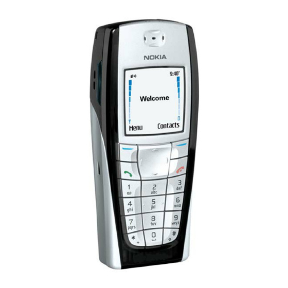
Nokia RH-27 Series Technical Documentation Manual
System module
Hide thumbs
Also See for RH-27 Series:
- Technical documentation manual (60 pages) ,
- Troubleshooting manual (10 pages) ,
- Troubleshooting instructions (6 pages)

Related Manuals for Nokia RH-27 Series


Summary of Contents for Nokia RH-27 Series
- Page 1 CCS Technical Documentation RH-27 Series Transceivers System Module © 2003 Nokia Corporation Issue 1 11/2003 Confidential...
-
Page 2: Table Of Contents
System Connector ....................22 Mechanical Shielding....................22 EMC Strategy ......................22 Test Interfaces ......................23 Production / After Sales Interface ................23 Flash Interface ......................24 FBUS Interface......................24 BB_RF Interface Connections ...................25 © 2003 Nokia Corporation Page 2 Confidential Issue 1 11/2003... - Page 3 RF Functional Description ..................27 Circuit Diagrams and PWB Layout ................ 28 Receiver........................28 Frequency Synthesizers................... 28 Transmitter ......................29 Antenna ........................31 Software Compensations ...................32 RF Frequency Plan ....................32 DC Characteristics....................33 © 2003 Nokia Corporation Issue 1 11/2003 Confidential Page 3...
-
Page 4: Introduction
PWB ground openings. Heat generated by the circuitry is con- ducted out via the PWB ground planes. The RH-27 transceiver module is implemented on six layer FR-4 material PWB. © 2003 Nokia Corporation Page 4 Confidential... -
Page 5: Functional Description
ACTIVE mode and all functions are activated. Sleep mode is exited either by the expiration of a sleep clock counter in the UEM, or by some external interrupt generated by a charger connection, key press, or headset connection among other things. While in © 2003 Nokia Corporation Issue 1 11/2003 Confidential... -
Page 6: Rh-27 Bb Functional Blocks
• Memory Module • Keyboard (UI module) • External Audio Connector • IrDa Interface • Vibra • FM Radio • System Connector (Tomahawk) • PWB Strategy • EMC Strategy • Test Interface © 2003 Nokia Corporation Page 6 Confidential Issue 1 11/2003... -
Page 7: Uem And Upp
Battery BLD-3 Li-ion (inbox battery) is used as the main power source for RH-27. No other bat- tery packs are planned to be used. BLD-3 has the capacity of 780 mAh. © 2003 Nokia Corporation Issue 1 11/2003 Confidential Page 7... - Page 8 BSI and BTEMP pins of the battery connector. Phone has 100 kW pull- up resistors for these lines so that they can be read by A/D inputs in the phone. For safety © 2003 Nokia Corporation Page 8...
- Page 9 3-wire type chargers are supported. The operation of the charging circuit has been spec- ified to limit the power dissipation across the charge switch and to ensure safe operation in all modes. © 2003 Nokia Corporation Issue 1 11/2003 Confidential...
-
Page 10: Charger Detection
If the charger is identified and accepted, the appropriate charging algorithm is initiated. Charger Interface Protection In order to ensure safe operation with all chargers and in mis-use situations, charger © 2003 Nokia Corporation Page 10 Confidential Issue 1 11/2003... -
Page 11: Led Driver Circuit
Driver is controlled by the UEM via DLIGHT output. This signal is connected to driver EN- pin (on/off). It is possible to control the LED brightness by PWM to achieve smooth on/off operation. © 2003 Nokia Corporation Issue 1 11/2003 Confidential... -
Page 12: Lcd Display
Number of pixels 130 x 130 pixels Technology CSTN (color super twisted nematic) Operating temperature range C to +70 Main viewing direction 6 o’clock Illumination mode transflective Color tone Background: Neutral/Black © 2003 Nokia Corporation Page 12 Confidential Issue 1 11/2003... -
Page 13: Rf Interface Block
1.8V. It uses a multiplexed address and data bus to minimize the pin count of the device. Control signals are used to allow byte access to the device. Flash Memory Description The 64 Mbit density flash with 16-bit data access operates in both asynchronous random © 2003 Nokia Corporation Issue 1 11/2003 Confidential Page 13... -
Page 14: Flash Architecture
UEM (MICB1) provides bias voltage. The microphone input on the UEM is ESD protected. Spring contacts are used to connect the microphone to the main PWB. © 2003 Nokia Corporation Page 14 Confidential Issue 1 11/2003... - Page 15 RH-27. Audio amplifier is controlled by the UPP. Speaker capsule is mounted in the C-cover. Spring contacts are used to connect the IHF Speaker contacts to the main PWB. © 2003 Nokia Corporation Issue 1 11/2003 Confidential...
-
Page 16: External Audio Connector
Accessory Control Interface (ACI) for accessory insertion and removal detection and identification and authentication. ACI line is also used for accessory control purposes. • 4-wire fully differential stereo audio (used also FM-radio antenna connection) • 2-wire differential mic input © 2003 Nokia Corporation Page 16 Confidential Issue 1 11/2003... -
Page 17: External Microphone Connection
HeadInt signal when the plug is inserted. Audio Amplifier FM Radio VAFR Rout+ VAFL Rout- Lout+ Lout- MIC3P MIC3N SPKRout+ SPKRout - PhoneIN (HS) XEAR IHF Speaker PhoneIN (IHF) Figure 12: External earphone and IHF connections © 2003 Nokia Corporation Issue 1 11/2003 Confidential Page 17... -
Page 18: Irda Interface
MCUSW. Reference clock, 32kHz, is generated by the UPP CTSI block (routed from sleep clock). GenIO(3) FMClk XTAL2 UPP8M TEA5767 FMCtrlDa GenIO(12) FMCtrlClk GenIO(11) FMWrEn GenIO(8) Figure 13: FM radio digital interface connections © 2003 Nokia Corporation Page 18 Confidential Issue 1 11/2003... -
Page 19: System Connector (Tomahawk)
Vhead. Thereby the comparator output will be changed to high state causing an interrupt. If the accessory is removed, the voltage level of HeadInt increases again to VFLASH1.This © 2003 Nokia Corporation Issue 1 11/2003 Confidential... -
Page 20: Pwb Strategy
The PWB in RH-27 consists of a 6-layer board made up of FR4. Via types are through hole, laser, buried, and blind vias. The PWB build up is shown below: © 2003 Nokia Corporation Page 20 Confidential Issue 1 11/2003... -
Page 21: Pwb Immunity
This is applied for both internal and external microphone lines. © 2003 Nokia Corporation Issue 1 11/2003 Confidential... -
Page 22: Ear Lines
The baseband EMC strategy is divided into electrical and mechanical items. All electrical guide lines, clocks, and high-speed signals should be routed in inner layers and away from the PWB edges. Clock signals distributed to other circuits should have series resis- © 2003 Nokia Corporation Page 22 Confidential... -
Page 23: Test Interfaces
VPP is the Flash programming volt- age and MBUS/CLK line is used as Flash clock line during flashing of phone. © 2003 Nokia Corporation Issue 1 11/2003 Confidential... -
Page 24: Flash Interface
FBUS is an asynchronous data bus having separate TX and RX signals. Default bit rate of the bus is 115.2 kbit/s. FBUS is mainly used for controlling and programming phone in the production. This is the primary interface used in RH-27. © 2003 Nokia Corporation Page 24 Confidential... -
Page 25: Bb_Rf Interface Connections
0/1.8V TXP1 RFIC 10 us Low Band Tx enabled TXP2 RFIC 0/1.8V High Band Tx enabled BANDSEL RFIC 0/1.8V Rx Band select. Option for module LNA. Not used in Stella. © 2003 Nokia Corporation Issue 1 11/2003 Confidential Page 25... - Page 26 Timing resolution GSM1900 RFAUXCONV(2:0) RF_BB Analog Control Signals to/from UEM TXPWRDET TXP Det. 0.1-2.4 V 50 us Tx PWR Detector Signal to UEM VCTCXO 0.1-2.4 V Automatic Frequency Control for VCTCXO © 2003 Nokia Corporation Page 26 Confidential Issue 1 11/2003...
-
Page 27: Rf Functional Description
RF ASIC. Externally sourced key components are: • 19.44 MHz VCTCXO • 2 GHz UHF VCO • 800MHz PA • 1900MHz PA • Power detector module • 1900MHz LNA transistor • Duplexer low band © 2003 Nokia Corporation Issue 1 11/2003 Confidential Page 27... -
Page 28: Circuit Diagrams And Pwb Layout
A common 2GHz UHFVCO module is used for operation on both low and high band. Frequency divider by two is integrated in the RF ASIC. © 2003 Nokia Corporation Page 28 Confidential... -
Page 29: Transmitter
The typical insertion loss is about -4.0dB, and maximum less than -5.0dB. This filter hasrelatively high pass band ripple about 1.0-1.5dB, largest insertion being at high end of the band. The input and return losses are about -10dB. © 2003 Nokia Corporation Issue 1 11/2003 Confidential... - Page 30 Table 6: 800 MHz analog TX Power RF power at external Tuning target Testing limits (dB) level Antenna Pad (dBm) tolerant (dB) 24.8 +/- 0.25 0.5/-0.5 22.0 +/-0.5 +/-2.0 18.5 +/-0.5 +/-2.0 © 2003 Nokia Corporation Page 30 Confidential Issue 1 11/2003...
-
Page 31: Antenna
-4.7 +/-0.5 +/-2.0 *** 26.3 dBm for channel 1000 and 1998; 27.0 dBm for channel 2. Antenna The RH-27 antenna solution is an internal dual resonance PIFA antenna. This antenna © 2003 Nokia Corporation Issue 1 11/2003 Confidential Page 31... -
Page 32: Software Compensations
256.2 MHz 869.04 - 893.97 MHz CELL RX IF 30 kHz Steps CELL 128.1 MHz 1930.00 - 1989.95 MHz RX Q 128.1 MHz 50 kHz Steps Figure 18: RH-27 frequency plan © 2003 Nokia Corporation Page 32 Confidential Issue 1 11/2003... -
Page 33: Dc Characteristics
2.7 max 1 +/- 10% 1.3 - 5.0 1.3 - 3.7 3 +/- 4% 3.5 +/- 4% 5 +/- 3% VREFRF01 1.35 +/- 0.5% 0.12 0.05 0.05 VFLASH1 2.78 +/- 3% © 2003 Nokia Corporation Issue 1 11/2003 Confidential Page 33... - Page 34 RH-27 System Module CCS Technical Documentation © 2003 Nokia Corporation Page 34 Confidential Issue 1 11/2003...