Table of Contents
Advertisement
Quick Links
SERVICE MANUAL
Ver 1.1 2002. 11
• The CD section have no adjustments.
SPECIFICATIONS
System
Compact disc digital audio
system
Signal format system
NTSC/PAL switchable
Frequency response
20 – 20,000 Hz
Wow and flutter
Below the measurable limit
Signal-to-noise ratio
85 dB
Outputs
Audio outputs (left/right)
Video output
BUS control output
Power requirement
12 V DC car battery
(negative ground)
Current drain
0.9 A (during disc playback)
1.8 A (during loading or ejecting
a disc)
Operating temperature
–10 °C to +55 °C
Approx. 178 × 50 × 172 mm
Dimensions
(w/h/d)
Approx. 178 × 50 × 154 mm
Mounting Dimensions
(w/h/d)
Mass
Approx. 1.3 kg
Supplied accessories
Parts for installation and
connections (1 set)
Design and specifications are subject to c hange without notice .
Sony Corporation
9-874-103-02
2002K0400-1
e Vehicle Company
© 2002. 11
Published by Sony Engineering Corporation
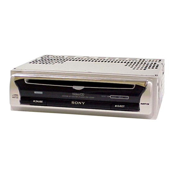
CSX-V58MP
Model Name Using Similar Mechanism
CD Drive Mechanism Type
Optical Pick-up Name
Features
• Sony BUS system compatible VCD/MP3
Player.
• MP3 file playback (recorded in the ISO9660
level 1 or 2 format, or Joliet or Romeo in the
expansion format or in Multi Session)
• CD-R/CD-RW which can have a session
added can be played.
• Discs recorded in Multi Session (CD-Extra,
Mixed mode CD, etc.) can be played,
depending on the recording method.
SYSTEM UP VCD/MP3 PLAYER
E Model
NEW
MG-383KA-121//K
KSS-720A
1
Advertisement
Table of Contents

Related Manuals for Sony CSX-V58MP


Summary of Contents for Sony CSX-V58MP
- Page 1 CD Drive Mechanism Type MG-383KA-121//K Optical Pick-up Name KSS-720A SPECIFICATIONS Features System Compact disc digital audio • Sony BUS system compatible VCD/MP3 Player. system Signal format system NTSC/PAL switchable • MP3 file playback (recorded in the ISO9660 Frequency response 20 – 20,000 Hz...
- Page 2 COMPONENTS IDENTIFIED BY MARK 0 OR DOTTED LINE WITH MARK 0 ON THE SCHEMATIC DIAGRAMS AND IN THE PARTS LIST ARE CRITICAL TO SAFE OPERATION. REPLACE THESE COMPONENTS WITH SONY PARTS WHOSE PART NUMBERS APPEAR AS SHOWN IN THIS MANUAL OR IN SUPPLEMENTS PUBLISHED BY SONY.
- Page 3 CSX-V58MP EXTENSION CABLE AND SERVICE POSITION When repairing or servicing this set, connect the jig (extension cable) as shown below. • Connect the MAIN board (CNP701) and the SERVO board (CN519) with the extension cable (Part No. J-2502-011-1). MAIN BOARD CNP701...
-
Page 4: Table Of Contents
CSX-V58MP TABLE OF CONTENTS 1. GENERAL ................5 2. DISASSEMBLY 2-1. Front Panel Assy ..............7 2-2. CD Mechanism Block ............8 2-3. Main Board ................. 8 2-4. Chassis (T) Sub Assy ............9 2-5. Lever Section ............... 9 2-6. Servo Board ............... 10 2-7. -
Page 5: General
Location of controls and indication lights CSX-V58MP 1 PAUSE indication lights up while the unit is pausing a disc. This unit must be connected to an optional Sony master unit with BUS control functions, such as the 2 DISC IN indication recommended Media Center/Receiver XAV-7W. - Page 6 Cautions Connection example (2) • This unit is designed for negative earth 12 V This unit must be connected to an optional Sony DC operation only. master unit with BUS control functions, such as • Do not get the wires under a screw, or caught Media Center/Receiver XAV-7W.
-
Page 7: Disassembly
CSX-V58MP SECTION 2 DISASSEMBLY Note : This equipment can be removed using the following procedure. 2-4. CHASSIS (T) SUB ASSY 2-1. FRONT PANEL ASSY (Page 9) (Page 7) 2-5. LEVER SECTION 2-6. SERVO BOARD 2-2. CD MECHANISM BLOCK (Page 9) -
Page 8: Cd Mechanism Block
CSX-V58MP 2-2. CD MECHANISM BLOCK 8 bracket (CD) 6 CD mechanism block 7 PTT 2.6x6 2 PTT 2.6x6 1 PTT 2.6x6 3 PTT 2.6x6 5 CNP701 2-3. MAIN BOARD 7 screw (+BTT) 8 screws (+BTT) 9 MAIN board 6 back chassis 5 PTT 2.6x6... -
Page 9: Chassis (T) Sub Assy
CSX-V58MP 2-4. CHASSIS (T) SUB ASSY 4 P 2x3 5 P 2x3 6 chassis (T) sub assy 3 Unsolder the lead wires. black white 2 heat sink (CD) 1 special screws 2-5. LEVER SECTION 5 guide (disc) 6 lever (R) -
Page 10: Servo Board
CSX-V58MP 2-6. SERVO BOARD 7 special screw 8 SERVO board 2 CN518 3 Removal the solders. 1 CN517 5 P 2x3 4 Unsolder the lead wires. 6 LO motor sub assy black (M903) yellow 2-7. SHAFT ROLLER ASSY, LOAD SW BOARD... -
Page 11: Floating Block Assy
CSX-V58MP 2-8. FLOATING BLOCK ASSY 6 floating block assy 7 compression spring (FL) 1 tension spring (KF1) 8 compression spring (FL) 4 Fit lever (D) in the direction of the arrow. 5 Turn loading ring in the direction of the arrow. -
Page 12: Diagrams
CSX-V58MP SECTION 3 DIAGRAMS 3-1. IC PIN DESCRIPTIONS • IC513 CXP81960M-672R (CD SYSTEM CONTROL) (SERVO BOARD (2/3)) Pin No. Pin Name Pin Description A_MUTE Audio mute control output — Not used. (Open) CD_ON CD servo power supply control output (H: Power on) - Page 13 CSX-V58MP Pin No. Pin Name Pin Description SENS Sensitivity input from DSP IC (IC516). IN_SW Disc in switch (SW3) input 65, 66 — Not used. (Connect to VDD in this set) MP3 playback control input (Fixed at L in this set)
- Page 14 CSX-V58MP • IC514 CL8830-PE0 (MPEG DECODER) (SERVO BOARD (3/3)) Pin No. Pin Name Pin Description RESERVED Not used. (Fixed at L in this set) 2 to 4 HDATA0 to 2 8-bit bi-directional host data bus 0 to 2 input/output for CD system control IC (IC513).
- Page 15 CSX-V58MP Pin No. Pin Name Pin Description MDATA7 Memory data 7 input/output LDQM SDRAM LDQM output for DRAM IC (IC520). UDQM SDRAM UDQM output for DRAM IC (IC520). — Power supply pin (+3.3 V) SDRAM write enable output for DRAM IC (IC520).
- Page 16 CSX-V58MP Pin No. Pin Name Pin Description — Ground RESERVED Not used. (Fixed at L in this set) VDATA3 Video data bus 3 output — Power supply pin (+3.3 V) VDATA4 Video data bus 4 output — Ground VDATA5 Video data bus 5 output RESERVED Not used.
- Page 17 CSX-V58MP Pin No. Pin Name Pin Description Host chip select input Read/write strobe input in I mode. Read strobe input in M mode.
- Page 18 SONY BUS serial output for BUS interface IC (IC803). UNI_CKI SONY BUS serial clock input from BUS interface IC (IC803). UNI_DATA_CHK SONY BUS serial data check input from BUS interface IC (IC803). LINK_OFF Link off output for bus interface IC (IC803). —...
-
Page 19: Circuit Boards Location
CSX-V58MP 3-2. CIRCUIT BOARDS LOCATION IN SELF SW board SL SW board SERVO board LOAD SW board MAIN board CONTROL board... -
Page 20: Block Diagram -Cd Section
CSX-V58MP 3-3. BLOCK DIAGRAM — CD SECTION — RF SIGNAL PROCESSOR IC516 IC511 RFAC RFAC SERIAL OPTICAL PICK-UP L-CH BLOCK MAIN (KSS-720A) SECTION A + B + C + D (Page 22) R-CH XTAI DA XCK RFDCO INV. IC515 MPEG... -
Page 21: Block Diagram -Mpeg Section
CSX-V58MP 3-4. BLOCK DIAGRAM — MPEG SECTION — MPEG DECODER IC514 Signal path CD-DATA CD-DA : CD AUDIO DA-DATA1 CD PCMD (Page 20) DA DATA CD-BCK DA-BCK CD BCK DA BCK : VIDEO SECTION CD-LRCK DA-LRCK CD LRCK DA LRCK... -
Page 22: Block Diagram -Main Section
CSX-V58MP 3-5. BLOCK DIAGRAM — MAIN SECTION — AUDIO AMP IC101 PJ101 (2/2) L-CH BUS AUDIO OUT SECTION (Page 20) R-CH MUTE Q103,203 D801 D802 A MUTE MUTE DRIVE MPEG Q801,802 SECTION INITIAL BU CHECK (Page 21) MUTE +8.5V +8.5V REG... - Page 23 (RFDCO) IC514 CSX-V58MP with a BUS cable. Power voltage is dc 14.4V from ACC and BATT cords of the SONY BUS compatible master unit, etc. and fed with regulated dc power supply. 3Vp-p 3Vp-p • Voltages are taken with a VOM (Input impedance 10 MΩ).
-
Page 24: Printed Wiring Board -Cd Mechanism Section (1/2)
CSX-V58MP 3-6. PRINTED WIRING BOARD — CD MECHANISM SECTION (1/2) — • Refer to page 23 for Common Note on Printed Wiring Boards. • Semiconductor Location (Side B) Ref. No. Location D511 D516 IC513 IC519 IC520 IC521 IC551 Q511 Q513... -
Page 25: Printed Wiring Boards -Cd Mechanism Section (2/2)
CSX-V58MP 3-7. PRINTED WIRING BOARDS — CD MECHANISM SECTION (2/2) — • Refer to page 23 for Common Note on Printed Wiring Boards. OPTICAL PICK-UP BLOCK (KSS-720A) • Semiconductor Location (Side A) Ref. No. Location D515 IC511 IC512 IC514 IC515... -
Page 26: Schematic Diagram -Cd Mechanism Section (1/3)
CSX-V58MP 3-8. SCHEMATIC DIAGRAM — CD MECHANISM SECTION (1/3) — • Refer to page 23 for Common Note on Schematic Diagram and Waveforms, refer to page 32 for IC Block Diagrams. IC B/D C551 R581 R514 R503 C613 R583 C513... -
Page 27: Schematic Diagram -Cd Mechanism Section (2/3)
CSX-V58MP 3-9. SCHEMATIC DIAGRAM — CD MECHANISM SECTION (2/3) — • Refer to page 23 for Common Note on Schematic Diagram and Waveforms, refer to page 32 for IC Block Diagrams. (Page 26) D515 CN519 IC523 R547 R546 R545 R639... -
Page 28: Schematic Diagram -Cd Mechanism Section (3/3)
CSX-V58MP 3-10. SCHEMATIC DIAGRAM — CD MECHANISM SECTION (3/3) — • Refer to page 23 for Common Note on Schematic Diagram and Waveforms. (Page 27) RB533 RB534 RB518 C617 R594 R682 JR507 IC520 IC521 C607 R684 R681 R685 C599 R680... -
Page 29: Printed Wiring Board -Main Section
CSX-V58MP 3-11. PRINTED WIRING BOARD — MAIN SECTION — • Refer to page 23 for Common Note on Printed Wiring Boards. PJ101 PJ102 CN101 • Semiconductor Location C305 R984 Ref. No. Location MF101 C984 R983 D304 Q984 D305 D306 C304... -
Page 30: Schematic Diagram -Main Section
CSX-V58MP 3-12. SCHEMATIC DIAGRAM — MAIN SECTION — • Refer to page 23 for Common Note on Schematic Diagram, refer to page 32 for IC Block Diagrams. IC B/D • Waveform (Main board) 4Vp-p Note: • Voltage is dc with respect to ground under no-signal 8.38MHz... -
Page 31: Printed Wiring Board -Control Section
CSX-V58MP 3-13. PRINTED WIRING BOARD — CONTROL SECTION — • Refer to page 23 for Common Note on Printed Wiring Boards. (Page 29) • Semiconductor Location Ref. No. Location LD501 LD502 LD503 D-11 LD504 C-11 LD505 C-12 LD506 C-13 3-14. SCHEMATIC DIAGRAM — CONTROL SECTION — • Refer to page 23 for Common Note on Schematic Diagram. -
Page 32: Ic Block Diagrams
CSX-V58MP 3-15. IC BLOCK DIAGRAMS IC511 CXA2570N-T4 IC512 LA6576L-TE-L IC518 STV0119B-TR VSYNC/ ODDEVEN 24 RFDCI S-GND CTRL+CFG 23 RFDCO CSI2C INPUT REGISTER CH2-CH4 OUTPUT 35 MUTE2 SYNC CONTROL MUTE2 ON/OFF RESET & HSYNC VIDEO TIMING CKREF GENERATOR CH1 OUTPUT VCC2... - Page 33 CSX-V58MP IC516 CXD2598Q 79 78 77 76 75 74 73 72 71 70 69 68 67 66 65 64 63 61 60 59 54 53 52 51 CLOCK GENERATOR BCKI ENPH EMPHI OP AMP ANALOG XVDD CONVERTER SWITCH SERIAL-IN DIGITAL...
-
Page 34: Exploded Views
CSX-V58MP SECTION 4 EXPLODED VIEWS NOTE: The components identified by mark 0 or • The mechanical parts with no reference • Color Indication of Appearance Parts dotted line with mark 0 are critical for number in the exploded views are not supplied. -
Page 35: Cd Mechanism Section (1)
CSX-V58MP Ver 1.1 4-2. CD MECHANISM SECTION (1) (MG-383KA-121//K) M903 Ref. No. Part No. Description Remark Ref. No. Part No. Description Remark * 51 1-676-709-11 IN SELF SW BOARD * 63 3-223-249-01 SHEET (HEAT SINK) 3-044-206-11 SCREW, SPECIAL 3-040-034-01 SPRING (RA), TENSION... -
Page 36: Cd Mechanism Section (2)
CSX-V58MP 4-3. CD MECHANISM SECTION (2) (MG-383KA-121//K) not supplied Ref. No. Part No. Description Remark Ref. No. Part No. Description Remark 3-040-025-02 ARM, CHUCKING 3-040-056-01 LEVER (D) 3-040-024-01 RETAINER (DISC) 3-040-057-01 LEVER (LOCK) 3-040-026-01 SPRING (CH), TENSION 3-040-052-01 WHEEL (U), WORM... -
Page 37: Cd Mechanism Section (3)
CSX-V58MP 4-4. CD MECHANISM SECTION (3) (MG-383KA-121//K) (including M901) M901 M902 The components identified by mark 0 or dotted line with mark 0 are critical for safety. Replace only with part number specified. Ref. No. Part No. Description Remark Ref. No. -
Page 38: Electrical Parts List
CSX-V58MP SECTION 5 CONTROL IN SELF SW ELECTRICAL PARTS LIST LOAD SW MAIN NOTE: The components identified by mark 0 or • Due to standardization, replacements in • Items marked “*” are not stocked since dotted line with mark 0 are critical for the parts list may be different from the they are seldom required for routine service. - Page 39 CSX-V58MP MAIN Ref. No. Part No. Description Remark Ref. No. Part No. Description Remark C903 1-162-970-11 CERAMIC CHIP 0.01uF IC991 8-759-710-88 IC NJM431U C921 1-126-767-11 ELECT 1000uF C922 1-126-176-11 ELECT 220uF < COIL > C923 1-107-826-11 CERAMIC CHIP 0.1uF C925 1-107-826-11 CERAMIC CHIP 0.1uF...
- Page 40 CSX-V58MP Ver 1.1 SERVO MAIN Ref. No. Part No. Description Remark Ref. No. Part No. Description Remark R301 1-216-841-11 METAL CHIP 1/10W A-3274-541-A SERVO BOARD, COMPLETE R304 1-216-809-11 METAL CHIP 1/10W ********************** R801 1-216-849-11 METAL CHIP 220K 1/10W R802 1-216-833-11 METAL CHIP 1/10W <...
- Page 41 CSX-V58MP SERVO Ref. No. Part No. Description Remark Ref. No. Part No. Description Remark C568 1-162-919-11 CERAMIC CHIP 22PF < FERRITE BEAD > C569 1-164-156-11 CERAMIC CHIP 0.1uF C570 1-163-234-11 CERAMIC CHIP 20PF FB511 1-469-144-21 FERRITE, EMI (SMD) C571 1-162-969-11 CERAMIC CHIP 0.0068uF 10%...
- Page 42 CSX-V58MP SERVO Ref. No. Part No. Description Remark Ref. No. Part No. Description Remark R514 1-216-610-11 RES-CHIP 1/10W R586 1-216-834-11 METAL CHIP 1/10W R515 1-216-845-11 METAL CHIP 100K 1/10W R587 1-216-834-11 METAL CHIP 1/10W R516 1-216-845-11 METAL CHIP 100K 1/10W...
- Page 43 CSX-V58MP SERVO SL SW Ref. No. Part No. Description Remark Ref. No. Part No. Description Remark R674 1-216-809-11 METAL CHIP 1/10W MISCELLANEOUS R675 1-216-809-11 METAL CHIP 1/10W *************** R676 1-216-809-11 METAL CHIP 1/10W R677 1-216-809-11 METAL CHIP 1/10W X-3378-480-1 CHASSIS (OP) ASSY (including M901)
- Page 44 CSX-V58MP REVISION HISTORY Clicking the version allows you to jump to the revised page. Also, clicking the version at the upper on the revised page allows you to jump to the next revised page. Ver. Date Description of Revision 2002. 07 2002.