Table of Contents
Advertisement
SERVICE MANUAL
Ver. 1.0 2013.06
Note:
Be sure to keep your PC used for service and
checking of this unit always updated with the
latest version of your anti-virus software.
In case a virus affected unit was found during
service, contact your Service Headquarters.
• HCD-SBT100 is the compact disc receiver in CMT-SBT100.
• HCD-SBT100B is the compact disc receiver in CMT-SBT100B.
• HCD-SBT300W is the compact disc receiver in CMT-SBT300W.
• HCD-SBT300WB is the compact disc receiver in CMT-SBT300WB.
Amplifier section (North American model)
Frequency response:
AUDIO POWER SPECIFICATIONS
50 Hz – 20 kHz
POWER OUTPUT AND TOTAL HARMONIC
Signal-to-noise ratio:
DISTORTION:
More than 90 dB
(The United States model only)
With 6 ohm loads, both channels driven, from
Dynamic range:
120 - 10,000 Hz; rated 20 watts per channel
More than 90 dB
minimum RMS power, with no more than 0.7%
total harmonic distortion from 250 milliwatts to
Tuner section
rated output.
Power output (rated): 20 watts + 20 watts
AM tuner section
(at 6 ohms, 1 kHz, 1% THD)
(HCD-SBT100/SBT300W only):
RMS power output (reference): 25 watts + 25 watts
Tuning range:
(per channel at 6 ohms, 1 kHz)
European models:
531 kHz – 1,602 kHz (with 9 kHz tuning
Amplifier section (Other models)
interval)
Other models:
Power output (rated):
530 kHz – 1,710 kHz (with 10 kHz tuning
HCD-SBT100/SBT100B:
interval)
20 watts + 20 watts (at 6 ohms, 1 kHz, 1% THD)
531 kHz – 1,710 kHz (with 9 kHz tuning
HCD-SBT300W/SBT300WB:
interval)
25 watts + 25 watts (at 6 ohms, 1 kHz, 1% THD)
Antenna:
RMS power output (reference):
AM loop antenna
HCD-SBT100/SBT100B:
Intermediate frequency:
25 watts + 25 watts (per channel at 6 ohms,
400 kHz
1 kHz)
HCD-SBT300W/SBT300WB:
FM tuner section:
50 watts + 50 watts (per channel at 6 ohms,
FM stereo, FM superheterodyne tuner
1 kHz)
North American model:
Inputs/Outputs
Tuning range:
87.5 MHz – 108.0 MHz (100 kHz step)
AUDIO IN:
Other models:
AUDIO IN (external input) jack:
Tuning range:
Stereo mini jack, sensitivity 700 mV,
87.5 MHz – 108.0 MHz (50 kHz step)
impedance 47 kilohms
(headphone) jack:
Antenna:
Stereo mini jack, 8 ohms or more
FM lead antenna
USB:
DAB/DAB+ tuner section
(HCD-SBT100B/SBT300WB only):
Supported bit rate:
FM stereo, DAB/FM superheterodyne tuner
MP3 (MPEG 1 Audio Layer-3): 32 kbps - 320
Frequency range:
kbps, VBR
WMA: 48 kbps - 192 kbps, VBR
Band-III:
AAC: 48 kbps -320 kbps
174.928 (5A) MHz – 239.200 (13F) MHz*
* For details, see "DAB/DAB+ frequency table"
Sampling frequencies:
below.
MP3 (MPEG 1 Audio Layer-3): 32/44.1/48 kHz
WMA: 44.1 kHz
Antenna:
AAC: 44.1 kHz
DAB/FM lead antenna:
USB port:
The DAB/DAB+ services are available only in
Type A, 5 V DC 2.1 A
countries/regions that support DAB/DAB+
services.
CD-DA/MP3 player section
System:
Compact disc and digital audio system
Laser Diode Properties:
Emission Duration: Continuous
Laser Output*: Less than 44.6 μW
* This output is the value measurement at a
distance of 200mm from the objective lens
surface on the Optical Pick-up Block with 7mm
aperture.
9-893-759-01
Sony Corporation
2013F33-1
©
2013.06
Published by Sony Techno Create Corporation
HCD-SBT100/SBT100B/
SBT300W/SBT300WB
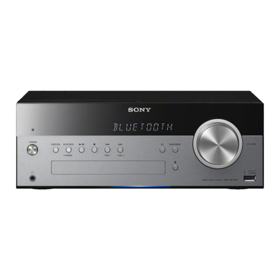
Photo: HCD-SBT300WB
Model Name Using Similar Mechanism
CD Mechanism Type
Optical Pick-up Block Name
SPECIFICATIONS
DAB/DAB+ frequency table (Band-III):
BLUETOOTH section
Frequency
Label
Communication system:
174.928 MHz
5A
BLUETOOTH Standard version 3.0
176.640 MHz
5B
Output:
178.352 MHz
5C
BLUETOOTH Standard Power Class 2
180.064 MHz
5D
Maximum communication range:
181.936 MHz
6A
Line of sight approx. 10 m
183.648 MHz
6B
Frequency band:
185.360 MHz
6C
2.4 GHz band (2.4000 GHz - 2.4835 GHz)
187.072 MHz
6D
Modulation method:
188.928 MHz
7A
FHSS
190.640 MHz
7B
Compatible BLUETOOTH profiles
192.352 MHz
7C
A2DP (Advanced Audio Distribution Profile)
AVRCP (Audio Video Remote Control Profile)
194.064 MHz
7D
195.936 MHz
8A
Supported content protection method
SCMS-T method
197.648 MHz
8B
199.360 MHz
8C
Transmission bandwidth
20 Hz – 20,000 Hz (with 44.1 kHz sampling)
201.072 MHz
8D
*
202.928 MHz
9A
204.640 MHz
9B
206.352 MHz
9C
208.064 MHz
9D
*
209.936 MHz
10A
211.648 MHz
10B
213.360 MHz
10C
Network section
215.072 MHz
10D
(HCD-SBT300/SBT300WB only)
216.928 MHz
11A
218.640 MHz
11B
LAN port:
RJ-45
220.352 MHz
11C
10BASE-T/100BASE-TX
222.064 MHz
11D
(The communication speed may vary
depending on the communication
223.936 MHz
12A
environment. This system does not
225.648 MHz
12B
guarantee the communication speed and
227.360 MHz
12C
quality of 10BASE-T/100BASE-TX.)
229.072 MHz
12D
230.784 MHz
13A
232.496 MHz
13B
234.208 MHz
13C
235.776 MHz
13D
237.488 MHz
13E
239.200 MHz
13F
* Frequencies are displayed to two decimal
places on this system.
Canadian Model
AEP Model
HCD-SBT100/SBT100B/
SBT300W/SBT300WB
HCD-SBT100B/SBT300WB
Australian Model
HCD-SBT100/SBT300W/SBT300WB
Wireless LAN:
Compatible standards:
IEEE 802.11 b/g (WEP 64 bit, WEP 128 bit)
Frequency band 2.4 GHz band (2.4000 GHz -
2.4835 GHz)
Available channels ch1 to ch13
WPA/WPA2-PSK (AES)
WPA/WPA2-PSK (TKIP)
*1
General
Power requirements:
North American model:
AC 120 V, 60 Hz
*2
Other models:
:
AC 220 V - 240 V, 50 Hz/60 Hz
Power consumption:
35 watts (HCD-SBT100/SBT100B)
36 watts (HCD-SBT300W/SBT300WB)
Dimensions (W/H/D) (incl. projecting parts,
excluding speakers):
1
The actual range will vary depending on factors
Approx. 290 mm × 106 mm × 221 mm
such as obstacles between devices, magnetic
Mass (excluding speakers):
fields around a microwave oven, static
electricity, reception sensitivity, antenna's
Approx. 2.7 kg
performance, operating system, software
application, etc.
Design and specifications are subject to
2
BLUETOOTH standard profiles indicate the
change without notice.
purpose of BLUETOOTH communication
between devices.
Standby power consumption: 0.5 W
COMPACT DISC RECEIVER
US Model
HCD-SBT100
UK Model
NEW
CDM90-DVBU202
CMS-S76RFS7G
Advertisement
Table of Contents

Related Manuals for Sony HCD-SBT100


Summary of Contents for Sony HCD-SBT100
- Page 1 In case a virus affected unit was found during service, contact your Service Headquarters. • HCD-SBT100 is the compact disc receiver in CMT-SBT100. Model Name Using Similar Mechanism • HCD-SBT100B is the compact disc receiver in CMT-SBT100B.
- Page 2 2 V AC range are suitable. (See registered trademarks owned by BLUETOOTH Fig. A) SIG, Inc. and any use of such marks by Sony Corporation is under license. Other trademarks and trade names are those of their respective To Exposed Metal owners.
-
Page 3: Table Of Contents
5-18. Schematic Diagram - FL Board - ........45 2-13. Chassis (Main) Block-2 ..........17 5-19. Printed Wiring Boards - KEY/ILLUMI Boards - ... 46 2-14. TUNER Board (HCD-SBT100/SBT300W) ....18 5-20. Schematic Diagram - KEY/ILLUMI Boards - ....47 2-15. Module (DAB Tuner) (DAB1), DAB Board 5-21. -
Page 4: Servicing Notes
NOTE OF REPLACING THE DAB BOARD When the DAB board is defective, exchange the complete mount- Model Part No. ed board. HCD-SBT100: AEP model 4-462-108-0[] HCD-SBT100: US model 4-462-108-1[] NOTE OF REPLACING THE MS-476 BOARD When the MS-476 board is defective, exchange the CDM90 ASSY... - Page 5 MAC address fi ltering function of con- nected access point equipment please set it again. MAC address is possible to confi rm it on the Sony Network Device Setting screen. Please refer to “Network connections” on the operating instructions for details.
- Page 6 HCD-SBT100/SBT100B/SBT300W/SBT300WB HOW TO OPEN THE TRAY WHEN POWER SWITCH TURN OFF Note 1: After the case is removed, this work is done. Note 2: Please prepare the thin wire (clip etc. processed to the length of 8 cm or more).
- Page 7 HCD-SBT100/SBT100B/SBT300W/SBT300WB FL, HP, KEY BOARDS SERVICE POSITION HP board FL board KEY board ILLUMI board USB board insulating sheet MAIN, POWER BOARDS SERVICE POSITION MAIN board POWER board...
-
Page 8: Disassembly
2-10. WiFi MODULE (WIFI1), NET BOARD (HCD-SBT300W/ 2-13. CHASSIS (MAIN) BLOCK-2 SBT300WB) (Page 17) (Page 14) 2-14. TUNER BOARD (HCD-SBT100/SBT300W) (Page 18) 2-15. MODULE (DAB TUNER) (DAB1), DAB BOARD (HCD-SBT100B/SBT300WB) (Page 18) 2-16. MAIN BOARD (Page 19) 2-17. POWER CORD (AC1) (Page 19) 2-18. -
Page 9: Case Block
HCD-SBT100/SBT100B/SBT300W/SBT300WB Note: Follow the disassembly procedure in the numerical order given. 2-2. CASE BLOCK 4 case block 1 three screws (BVTP S3 1 screw (BVTP S3 3 Remove the case block in the 1 screw direction of an arrow. (BVTP S3 2-3. -
Page 10: Flexible Flat Cable (19P) (Ffc6) (Hcd-Sbt300W/Sbt300Wb)
HCD-SBT100/SBT100B/SBT300W/SBT300WB 2-4. FLEXIBLE FLAT CABLE (19P) (FFC6) (HCD-SBT300W/SBT300WB) 15 to 20 mm cushion (S) ferrite core (FC3) ferrite core (FC4) cushion (S) 15 to 20 mm flexible flat cable (19P) (FFC6) NET board tape WiFi module (sub material) tape (sub material) -
Page 11: Tape (Sub Material)
HCD-SBT100/SBT100B/SBT300W/SBT300WB 2-5. TAPE (SUB MATERIAL) 1 tape (sub material) tape (sub material) 3 tape 4 tape 5 tape (sub material) (sub material) (sub material) 3 tape (sub material) 3 tape (sub material) 6 tape (sub material) 2 tape (sub material) -
Page 12: Panel (Front) Block-1
HCD-SBT100/SBT100B/SBT300W/SBT300WB 2-6. PANEL (FRONT) BLOCK-1 Note 1: CN106 and CN340 are quantity of pins of the same. Do not insert to the wrong connector absolutely. There is a possibility that the unit may be damaged if the wrong. coating clip... -
Page 13: Panel (Front) Block-2
HCD-SBT100/SBT100B/SBT300W/SBT300WB 2-7. PANEL (FRONT) BLOCK-2 5 panel (front) block Note: Arrange the wire so as not to overlap 2 two screws with the screw hole of HP board. (BV3) 4 Draw out the wire. 1 screw (BVTP S3 1 screw... -
Page 14: Net Board Block (Hcd-Sbt300W/Sbt300Wb)
HCD-SBT100/SBT100B/SBT300W/SBT300WB 2-9. NET BOARD BLOCK (HCD-SBT300W/SBT300WB) tape 1 antenna connector (sub material) NET board (CON2) antenna wire 5 NET board block Note: Arrange the antenna wire so as not to overlap with the screw hole of panel (rear). 3 two screws... -
Page 15: Ghz Antenna (Ant1), Holder (Antenna) (Hcd-Sbt300W/Sbt300Wb)
HCD-SBT100/SBT100B/SBT300W/SBT300WB 2-11. 2.4GHz ANTENNA (ANT1), HOLDER (ANTENNA) (HCD-SBT300W/SBT300WB) tape (sub material) NET board antenna wire Note: Arrange the antenna wire so as not to overlap claw with the screw hole of panel (rear). 1 antenna connector 2 tape (CON2) (sub material) 4 2.4GHz antenna... -
Page 16: Chassis (Main) Block-1
HCD-SBT100/SBT100B/SBT300W/SBT300WB 2-12. CHASSIS (MAIN) BLOCK-1 Note 1: CN3002 and CN507 are quantity of pins of the same. Do not insert to the wrong connector absolutely. There is a possibility that the unit may be damaged if the wrong. Wire e i... -
Page 17: Chassis (Main) Block-2
HCD-SBT100/SBT100B/SBT300W/SBT300WB 2-13. CHASSIS (MAIN) BLOCK-2 Note 3: When installing the flexible flat cable, Note 1: Before disconnecting flexible flat cable (24P) (CN501), solder the short-land. ensure the colored line. No slanting after insertion. Inserting is straight to the interior. (SBT300W/... -
Page 18: Tuner Board (Hcd-Sbt100/Sbt300W)
HCD-SBT100/SBT100B/SBT300W/SBT300WB 2-14. TUNER BOARD (HCD-SBT100/SBT300W) Note: When installing the flexible flat cable, ensure the colored line. No slanting after insertion. flexible flat cable (9P) (FFC3) Inserting is straight to the interior. flexible flat cable 5 flexible flat cable (9P) (CN101) -
Page 19: Main Board
HCD-SBT100/SBT100B/SBT300W/SBT300WB 2-16. MAIN BOARD 1 two screws (BVTP3 3 radiation sheet 2 heatsink (AMP) Tape materia etti 6 tape 4 screw (sub material) (BVTP3 ditch ditch tape tape 4 five screws (sub material) (sub material) (BVTP3 4 screw (BVTP3 4 screw... -
Page 20: Power Board
HCD-SBT100/SBT100B/SBT300W/SBT300WB 2-18. POWER BOARD 1 power cord connector (CN901) 2 screw (BV3) 2 three screws (BV3) 2 screw Note: When you install the connector, please (BV3) install them correctly. There is a possibility that this machine 6 POWER board damages when not correctly installing it. -
Page 21: Cd Mechanism Deck Block
HCD-SBT100/SBT100B/SBT300W/SBT300WB 2-19. CD MECHANISM DECK BLOCK 2 CD mechanism deck block 1 two screws (BV3) 1 two screws (BV3) 2-20. FFC HOLDER 1 tape (sub material) tape 4 FFC holder (sub material) Note: When installing the FFC holder, FFC holder check that installed firmly two bosses and claw. -
Page 22: Optical Pick-Up (Cms-S76Rfs7G) (Op1)
HCD-SBT100/SBT100B/SBT300W/SBT300WB 2-21. OPTICAL PICK-UP (CMS-S76RFS7G) (OP1) 2 chuck holder block 5 insulator screw 5 insulator screw 0 insulator qa optical pick-up 7 connector (CMS-S76RFS7G) (OP1) 0 insulator 5 insulator screw 0 insulator Wire 9 connector 5 insulator screw 0 insulator... -
Page 23: Test Mode
3. It enters the common test mode, the message “AUDIO IN” is seconds. displayed on the fl uorescent indicator tube. 3. The message “RESET” (HCD-SBT100/SBT100B) or “ALL (In this mode, “cPLAY” and “SLEEP” continues blinking on RESET” (HCD-SBT300W/SBT300WB) is displayed on the the liquid crystal display) fl... - Page 24 HCD-SBT100/SBT100B/SBT300W/SBT300WB 5. When pressing the [ TUNE +] button again, the MC ver- DISC TRAY LOCK MODE > sion is displayed on the fl uorescent indicator tube. It can be unable to take sample disc out of disc tray in the shop.
-
Page 25: Electrical Checks
HCD-SBT100/SBT100B/SBT300W/SBT300WB SECTION 4 ELECTRICAL CHECKS 0 dB = 1 μV TUNER SECTION CD SECTION Note: FM AUTO STOP CHECK 1. CD block is basically constructed to operate without adjustment. 2. Use HLX-A1 disc (Part No. J-2501-307-A) unless otherwise indicat- signal generator 3. - Page 26 HCD-SBT100/SBT100B/SBT300W/SBT300WB MEMO...
-
Page 27: Diagrams
HCD-SBT100/SBT100B/SBT300W/SBT300WB SECTION 5 DIAGRAMS 5-1. BLOCK DIAGRAM - CD Section - OPTICAL PICK-UP BLOCK RF AMP, SERVO/AUDIO PROCESSOR (CMS-S76RFS7G) IC501 ASDATA0, ABCK, ASDATA0 ALRCK, ACLK >001B (Page 28) 123 RFIP ASDATA0 ABCK ABCK VOA/A 1 RF_C ALRCK ALRCK VOB/B 128 RF_B... -
Page 28: Block Diagram - Audio Section
HCD-SBT100/SBT100B/SBT300W/SBT300WB 5-2. BLOCK DIAGRAM - AUDIO Section - DIGITAL AUDIO SELECTOR IC741 ASDATA0, ABCK, SAMPLE RATE CONVERTER AUDIO DSP STREAM PROCESSOR DIGITAL POWER AMP ALRCK, ACLK IC761 IC762 IC3005 IC3007 ASDATA0 >001B 6 1C0 5 1C1 (Page 27) A/D CONVERTER... -
Page 29: Block Diagram - Panel/Power Supply Section
HCD-SBT100/SBT100B/SBT300W/SBT300WB 5-3. BLOCK DIAGRAM - PANEL/POWER SUPPLY Section - REMOTE CONTROL RESET RECEIVER 4 SIRCS RESET IC102 IC5002 PROTECT DETECT B+ SWITCH SYSTEM PROTECT FLUORESCENT INDICATOR TUBE DRIVER, Q911 Q912, 913 D914 LED DRIVER IC5001 SG1 – SG16 54 DP DI... - Page 30 HCD-SBT100/SBT100B/SBT300W/SBT300WB THIS NOTE IS COMMON FOR PRINTED WIRING BOARDS AND SCHEMATIC DIAGRAMS. • Circuit Boards Location (In addition to this, the necessary note is printed in each block.) For Printed Wiring Boards. For Schematic Diagrams. Note: Note: TUNER board (SBT100/SBT300W) •...
-
Page 31: Schematic Diagram - Main Section (1/7)
HCD-SBT100/SBT100B/SBT300W/SBT300WB 5-4. SCHEMATIC DIAGRAM - MAIN Section (1/7) - • See page 50 for Waveforms. • See page 52 for IC Block Diagrams. • See page 60 for IC Pin Function Description. (Page 34) MAIN BOARD (1/7) ASDATA0 CL560 >103S... -
Page 32: Schematic Diagram - Main Section (2/7)
HCD-SBT100/SBT100B/SBT300W/SBT300WB 5-5. SCHEMATIC DIAGRAM - MAIN Section (2/7) - • See page 52 for IC Block Diagrams. MAIN BOARD (2/7) IC841 R881 R884 C880 R889 R888 R887 R897 R898 R899 C890 R894 DC/DC CONVERTER R880 IC841 BD00GA3WEFJ-E2 (3.3) (3.1) CL840 R891 (3.2) -
Page 33: Schematic Diagram - Main Section (3/7)
HCD-SBT100/SBT100B/SBT300W/SBT300WB 5-6. SCHEMATIC DIAGRAM - MAIN Section (3/7) - • See page 52 for IC Block Diagrams. MAIN BOARD (3/7) >109S (Page 36) (SBT100/SBT300W) MAIN BOARD (6/7) CN251 FB405 TUNER-P CL251 IISD CL252 R298 FFC3 CL253 LRCK CL254 (SBT100/SBT300W) C278... -
Page 34: Schematic Diagram - Main Section (4/7)
HCD-SBT100/SBT100B/SBT300W/SBT300WB 5-7. SCHEMATIC DIAGRAM - MAIN Section (4/7) - • See page 50 for Waveforms. • See page 52 for IC Block Diagrams. • See page 60 for IC Pin Function Description. MAIN BOARD (4/7) (Page 35) DAMP-SDA >114S DAMP-SCLK... -
Page 35: Schematic Diagram - Main Section (5/7)
HCD-SBT100/SBT100B/SBT300W/SBT300WB 5-8. SCHEMATIC DIAGRAM - MAIN Section (5/7) - • See page 50 for Waveforms. • See page 52 for IC Block Diagrams. MAIN BOARD (5/7) (Page 36) R3004 R3005 R3085 >116S DAMP-RST R3006 R3027 PG_MUTE MAIN Q3005 R3007 (Page... -
Page 36: Schematic Diagram - Main Section (6/7)
HCD-SBT100/SBT100B/SBT300W/SBT300WB 5-9. SCHEMATIC DIAGRAM - MAIN Section (6/7) - • See page 50 for Waveforms. • See page 52 for IC Block Diagrams. • See page 60 for IC Pin Function Description. MAIN BOARD (6/7) D102 BAV99-215 R206 R228 (SBT300W/SBT300WB) (SBT300W/SBT300WB) 2.2k (SBT100: US, CND) -
Page 37: Schematic Diagram - Main Section (7/7)
HCD-SBT100/SBT100B/SBT300W/SBT300WB 5-10. SCHEMATIC DIAGRAM - MAIN Section (7/7) - • See page 50 for Waveforms. • See page 52 for IC Block Diagrams. MAIN BOARD (7/7) (Page 48) CN304 JL901 >06S (Page 34) R997 V2_GND CL901 V2_12-17V >115S POWER BOARD... -
Page 38: Printed Wiring Boards - Main Section (1/2)
HCD-SBT100/SBT100B/SBT300W/SBT300WB 5-11. PRINTED WIRING BOARDS - MAIN Section (1/2) - • See page 30 for Circuit Boards Location. • : Uses unleaded solder. (Page 40) MAIN BOARD USB BOARD >01P CN5012 (COMPONENT SIDE) (CHASSIS) (CHASSIS) (CHASSIS) (CHASSIS) FFC4 CL5087 D5001... -
Page 39: Printed Wiring Board - Main Section (2/2)
HCD-SBT100/SBT100B/SBT300W/SBT300WB 5-12. PRINTED WIRING BOARD - MAIN Section (2/2) - • See page 30 for Circuit Boards Location. • : Uses unleaded solder. J5001 TB3001 AUDIO IN SPEAKERS – – MAIN BOARD (CONDUCTOR SIDE) R3113 R5042 C3117 C3115 C3116 R3114... -
Page 40: Printed Wiring Boards - Usb/Hp/Relay Boards
HCD-SBT100/SBT100B/SBT300W/SBT300WB 5-13. PRINTED WIRING BOARDS - USB/HP/RELAY Boards - • See page 30 for Circuit Boards Location. • : Uses unleaded solder. USB BOARD HP BOARD (COMPONENT SIDE) CL5080 JL5004 CL5081 JL309 C5029 IC5005 CN5008 FB251 R260 R5160 JL5007 C5027... -
Page 41: Schematic Diagram - Usb/Hp/Relay Boards
HCD-SBT100/SBT100B/SBT300W/SBT300WB 5-14. SCHEMATIC DIAGRAM - USB/HP/RELAY Boards - • See page 50 for Waveforms. • See page 52 for IC Block Diagrams. USB BOARD HP BOARD CN5012 R304 CL5086 (Page 35) NO301 PROTECT R260 CL5109 JL309 VBUSP-MONI >02S CL5084 HP-DET... -
Page 42: Printed Wiring Board
HCD-SBT100/SBT100B/SBT300W/SBT300WB 5-15. PRINTED WIRING BOARD - NET Board (HCD-SBT300W/SBT300WB) - • See page 30 for Circuit Boards Location. • : Uses unleaded solder. NET BOARD (COMPONENT SIDE) CL5070 C5018 R5150 C5055 R5069 FB5007 C5014 R5001 C5011 C5010 CN5001 C5001 C5013... -
Page 43: Schematic Diagram
HCD-SBT100/SBT100B/SBT300W/SBT300WB 5-16. SCHEMATIC DIAGRAM - NET Board (HCD-SBT300W/SBT300WB) - • See page 52 for IC Block Diagrams. NET BOARD CN5001 ANT1 R5001 CL5001 3.3VCC CL5002 R5011 C5003 R5091 C5064 RXD0 WIFI1 0.047 CL5003 WIFI MODULE TXD0 (NC) CL5004 R5092 CN5002... -
Page 44: Printed Wiring Board - Fl Board
HCD-SBT100/SBT100B/SBT300W/SBT300WB 5-17. PRINTED WIRING BOARD - FL Board - • See page 30 for Circuit Boards Location. • : Uses unleaded solder. (Page 46) ILLUMI BOARD >09P CN3001 FFC11 CN5003 T5001 (Page 38) JW5029 MAIN BOARD >05P CN506 FFC8 S5001... -
Page 45: Schematic Diagram - Fl Board
HCD-SBT100/SBT100B/SBT300W/SBT300WB 5-18. SCHEMATIC DIAGRAM - FL Board - • See page 50 for Waveforms. • See page 52 for IC Block Diagrams. FL BOARD ND5001 FLUORESCENT INDICATOR TUBE 10 11 12 13 14 15 35 36 37 38 39 40 41 42 43 44 45 46 47 48 49 50... -
Page 46: Printed Wiring Boards - Key/Illumi Boards
HCD-SBT100/SBT100B/SBT300W/SBT300WB 5-19. PRINTED WIRING BOARDS - KEY/ILLUMI Boards - • See page 30 for Circuit Boards Location. • : Uses unleaded solder. S3202 KEY BOARD R3202 R3102 R3105 C3201 R3204 S3101 R3104 R3203 S3106 C3102 S3105 S3104 S3103 S3206 S3205... -
Page 47: Schematic Diagram - Key/Illumi Boards
HCD-SBT100/SBT100B/SBT300W/SBT300WB 5-20. SCHEMATIC DIAGRAM - KEY/ILLUMI Boards - KEY BOARD Q3101 PDTC114ET R3102 R3104 R3105 LED DRIVE 2.2k 2.2k C3102 S3101 S3103 S3104 S3105 S3106 BLUETOOTH FUNCTION D3101 PARING SLR-325VCT31P STANDBY CN3101 R3206 R3103 CL3101 1.5k STBY-R CL3102 EVER_3.3V D3201... -
Page 48: Schematic Diagram - Power Board
HCD-SBT100/SBT100B/SBT300W/SBT300WB 5-21. SCHEMATIC DIAGRAM - POWER Board - • See page 52 for IC Block Diagrams. POWER BOARD F901 CN901 LF901 LF902 250V TH901 JL901 JL902 LINE FILTER LINE FILTER D902 LIVE D3SB60F3 D968 (Page 41) JL903 (AC IN) FMX-22SL... -
Page 49: Printed Wiring Board - Power Board
HCD-SBT100/SBT100B/SBT300W/SBT300WB 5-22. PRINTED WIRING BOARD - POWER Board - • See page 30 for Circuit Boards Location. • : Uses unleaded solder. (AC IN) POWER BOARD CN901 C905 R901 VDR901 ET902 JL901 CAM902 PATTERN SPARK-GAP (CHASSIS) F901 CL905 C903 C907... - Page 50 HCD-SBT100/SBT100B/SBT300W/SBT300WB • Waveforms – MAIN Board – IC762 ql (LRCK) IC501 8 (XTALO) IC101 qd (Xout) 1.3 Vp-p 3.2 Vp-p 3.7 Vp-p 37 ns 20.8 s 200 ns 2 V/DIV, 10 s/DIV 1 V/DIV, 20 ns/DIV 2 V/DIV, 100 ns/DIV IC501 <zzx (ACLK)
- Page 51 HCD-SBT100/SBT100B/SBT300W/SBT300WB – USB Board – – FL Board – IC5008 1 (BOOT) IC5001 5 (OSC) 16.4 Vp-p 2.2 Vp-p 300 s 2.2 s 10 V/DIV, 200 s/DIV 1 V/DIV, 2 s/DIV Q5003 (Base) 3.8 Vp-p 11.3 s 2 V/DIV, 5 s/DIV...
- Page 52 HCD-SBT100/SBT100B/SBT300W/SBT300WB • IC Block Diagrams – MAIN Board – IC103, 105, 107, 905, 3001 MM3411A33NRE VDD 1 GND 2 VOUT CURRENT LIMIT VOLTAGE REFERENCE CE 3 BIAS IC202 TC74VHC4066AFK (EK) 1I/O 1O/I 2 2O/I 3 2I/O 4 2C 5 4I/O...
- Page 53 HCD-SBT100/SBT100B/SBT300W/SBT300WB IC503 MM3374A33PRE VOUT CE 1 BIAS THERMAL CURRENT VOLTAGE SHUTDOWN LIMIT REFERENCE GND 2 NC 3 IC561 MM1701CHBE IC702, 841 BD00GA3WEFJ-E2 VOUT 8 VIN 7 NC 6 NC BIAS 5 CONT CURRENT DRIVER LIMITTER SOFT REFERENCE THERMAL SHUTDOWN IC721 PCM1808PWR...
- Page 54 HCD-SBT100/SBT100B/SBT300W/SBT300WB IC741, 742 TC74VHC153FT (EL) DATA INPUTS STROBE OUTPUT 2C2 2C1 2C0 SELECT 2C3 2C2 2C1 2C0 1C3 1C2 1C1 1C0 STROBE 1C3 1C2 1C1 1C0 OUTPUT SELECT DATA INPUTS IC743 TC74VHC257FT (EL) SELECT 1 1A 2 1B 3 1Y 4...
- Page 55 HCD-SBT100/SBT100B/SBT300W/SBT300WB IC851 AM5890S MUTE MUTE BIAS VINFC 1 VINTK TRB1 2 REGO2 3 TRB2 VOLTAGE RESET DETECTION VINSL+ 4 VINLD REGO1 5 VCTL VCCD FWD 6 VCC2 DRIVER REV 7 VCC2 SPINDLE VOLD– VCC1 DRIVER (4x) VCC2 VOLD+ VCC1 VOTK–...
- Page 56 HCD-SBT100/SBT100B/SBT300W/SBT300WB IC3003 MM3411A18URE CE 1 BIAS VOLTAGE – REFERENCE CURRENT LIMIT VOUT GND 2 IC3005 CXD9843AR CLOCK CLOCK GENERATOR 36 XFSIIN GENERATOR (SECONDARY) (PRIMARY) XVSS 35 DVDD VSUBC 34 TEST 33 BFVSS VSSR OUTR2 32 BFVDD VDDR DATA OUTR1 FILTER &...
- Page 57 HCD-SBT100/SBT100B/SBT300W/SBT300WB IC3007 TAS5614APHDR GND_A GND_D PVDD_A PVDD_D PVDD_A PVDD_D OUT_A OUT_D OUT_A OUT_D BST_A BST_D GATE GATE GATE GATE DRIVE DRIVE DRIVE DRIVE GVDD_A GVDD_D GVDD_B GVDD_C TIMING TIMING TIMING TIMING CONTROL CONTROL CONTROL CONTROL CONTROL CONTROL CONTROL CONTROL RECEIVER...
- Page 58 HCD-SBT100/SBT100B/SBT300W/SBT300WB – USB Board – IC5005 TPS2561DRCR GND 1 CURRENT IN 2 SENSE IN 3 10 FAULT1 THERMAL SENSE 9 OUT1 CHARGE 9-ms PUMP DEGLITCH 8 OUT2 EN1 4 CURRENT 7 ILLM DRIVER EN2 5 LIMIT 6 FAULT2 UNDERVOLTAGE 9-ms...
- Page 59 HCD-SBT100/SBT100B/SBT300W/SBT300WB – FL Board – IC5001 PT6315-LQ (B) LED1 LED2 LED DRIVER LED3 DIMMING LED4 CIRCUIT 33 SG19/GR10 32 SG18/GR11 KEY MATRIX 31 SG17/GR12 MEMORY GRID DRIVER 30 VEE TIMING GENERATOR 29 SG16/KS16 28 SG15/KS15 27 SG14/KS14 DOUT SEGMENT DRIVER/...
- Page 60 DAB TxD-OUT Serial data output to the DAB board (HCD-SBT100B/SBT300WB) TUNER SCL/ Serial data transfer clock signal output to the TUNER board (HCD-SBT100/SBT300W) DAB RxD-IN Serial data input from the DAB board (HCD-SBT100B/SBT300WB) RDS interrupt signal input from the TUNER board (HCD-SBT100/SBT300W) RDS INT/ +3.3V power on/off control signal output to the DAB board for the DAB tuner section...
- Page 61 HCD-SBT100/SBT100B/SBT300W/SBT300WB Pin No. Pin Name Description WM SLEEP IN Sleep detection signal input terminal for the WALKMAN port Not used USB/UART SELECT USB/UART selection signal output terminal Not used WM POWER VBUS power on/off control signal output terminal for the WALKMAN section...
- Page 62 HCD-SBT100/SBT100B/SBT300W/SBT300WB MAIN BOARD IC501 CXD90013R (RF AMP, SERVO/AUDIO PROCESSOR) Pin No. Pin Name Description RF_C RF main beam (A) input from the optical pick-up block RF_D RF main beam (D) input from the optical pick-up block RF_E RF sub beam (F) input from the optical pick-up block...
- Page 63 HCD-SBT100/SBT100B/SBT300W/SBT300WB Pin No. Pin Name Description RCLK Clock signal output to the SD-RAM 73 to 79 RA11, RA9 to RA4 Address signal output to the SD-RAM RWE# Write enable signal output to the SD-RAM DVSS12 Ground terminal (digital system) CAS#...
- Page 64 HCD-SBT100/SBT100B/SBT300W/SBT300WB MAIN BOARD IC762 TAS3108DCPR (AUDIO DSP) Pin No. Pin Name Description AVSS Ground terminal (analog system) VR_PLL External capacitor connection terminal for internal regulator XTALI System clock input terminal (12.288 MHz) XTALO System clock output terminal (12.288 MHz) MCLKI...
-
Page 65: Exploded Views
HCD-SBT100/SBT100B/SBT300W/SBT300WB SECTION 6 EXPLODED VIEWS Note: • -XX and -X mean standardized parts, so • The mechanical parts with no reference The components identifi ed by mark 0 they may have some difference from the number in the exploded views are not sup- or dotted line with mark 0 are critical for original one. -
Page 66: Base (Cd) Section
HCD-SBT100/SBT100B/SBT300W/SBT300WB 6-2. BASE (CD) SECTION (SBT300W/SBT300WB) FFC6 – Left view – panel (back) section FL board section Ref. No. Part No. Description Remark Ref. No. Part No. Description Remark 4-462-088-01 PLATE (CD) ORNAMENT (SBT100/SBT100B) 1-457-414-11 CORE, FERRITE 4-462-088-11 PLATE (CD) ORNAMENT (SBT300W/SBT300WB) -
Page 67: Fl Board Section
HCD-SBT100/SBT100B/SBT300W/SBT300WB 6-3. FL BOARD SECTION • Rear view panel (front) section supplied with S5001 not supplied (ILLUMI board) not supplied (FL board) FFC4 S5001 not supplied not supplied (HP board) FFC11 not supplied (HOLDER board) FFC8 Ref. No. Part No. -
Page 68: Panel (Front) Section
HCD-SBT100/SBT100B/SBT300W/SBT300WB 6-4. PANEL (FRONT) SECTION • Rear view NFC1 FFC9 not supplied FFC7 155 155 not supplied FFC10 not supplied (KEY board) Ref. No. Part No. Description Remark Ref. No. Part No. Description Remark 3-087-053-01 +BVTP2.6 (3CR) X-2587-537-1 FRONT (SBT300WB) ASSY (SBT300WB: AEP, UK) -
Page 69: Panel (Back) Section
HCD-SBT100/SBT100B/SBT300W/SBT300WB 6-5. PANEL (BACK) SECTION • Rear view not supplied (RELAY board) not supplied (SBT300W/SBT300WB) WIFI1 ANT1 MAIN board section not supplied not supplied Note 1: When the complete NET board is replaced, refer to “CHECK- ING METHOD OF NETWORK CONNECTION” on page 5. -
Page 70: Main Board Section
HCD-SBT100/SBT100B/SBT300W/SBT300WB 6-6. MAIN BOARD SECTION not supplied (US, CND) not supplied not supplied not supplied (SBT300W/SBT300WB) chassis section Note: When the complete MAIN board is replaced, refer to “CHECKING METHOD OF NETWORK CONNECTION” on page 5. Ref. No. Part No. -
Page 71: Chassis Section
HCD-SBT100/SBT100B/SBT300W/SBT300WB 6-7. CHASSIS SECTION CD mechanism deck section (CDM90-DVBU202) not supplied (POWER board) not supplied (SBT100/SBT300W) FFC3 (SBT100B/SBT300WB) not supplied CN01 FFC5 not supplied DAB1 not supplied Ref. No. Part No. Description Remark Ref. No. Part No. Description Remark 4-427-514-01... -
Page 72: Cd Mechanism Deck Section (Cdm90-Dvbu202)
HCD-SBT100/SBT100B/SBT300W/SBT300WB 6-8. CD MECHANISM DECK SECTION (CDM90-DVBU202) not supplied CDM1 not supplied not supplied not supplied MS-476 not supplied board not supplied FFC2 FFC1 Ref. No. Part No. Description Remark Ref. No. Part No. Description Remark 2-634-618-21 INSULATOR FFC2 9-885-188-62 FY13 FFC (1.0 mm_5P_CDM) -
Page 73: Electrical Parts List
HCD-SBT100/SBT100B/SBT300W/SBT300WB SECTION 7 ELECTRICAL PARTS LIST Note: • Due to standardization, replacements in • CAPACITORS When indicating parts by reference num- uF: μF the parts list may be different from the ber, please include the board name. parts specifi ed in the diagrams or the com- •... - Page 74 HCD-SBT100/SBT100B/SBT300W/SBT300WB ILLUMI MAIN Ref. No. Part No. Description Remark Ref. No. Part No. Description Remark < TRANSFORMER > < CONNECTOR > T5001 1-697-285-11 DC-DC CONVERTERS CN3101 1-779-546-11 CONNECTOR, FFC (LIF (NON-ZIF)) 9P ************************************************************* < LED > HP BOARD ********* D3101...
- Page 75 HCD-SBT100/SBT100B/SBT300W/SBT300WB MAIN Ref. No. Part No. Description Remark Ref. No. Part No. Description Remark C104 1-125-777-11 CERAMIC CHIP 0.1uF C505 1-164-852-11 CERAMIC CHIP 12PF C106 1-100-916-11 CERAMIC CHIP 0.1uF C506 1-118-386-11 CERAMIC CHIP 0.1uF C107 1-100-916-11 CERAMIC CHIP 0.1uF C508 1-112-777-11 CERAMIC CHIP 0.01uF...
- Page 76 HCD-SBT100/SBT100B/SBT300W/SBT300WB MAIN Ref. No. Part No. Description Remark Ref. No. Part No. Description Remark C600 1-100-916-11 CERAMIC CHIP 0.1uF C910 1-164-870-11 CERAMIC CHIP 68PF C911 1-164-854-11 CERAMIC CHIP 15PF C706 1-165-908-11 CERAMIC CHIP 1uF C912 1-116-865-11 CERAMIC CHIP 10uF C708 1-100-916-11 CERAMIC CHIP 0.1uF...
- Page 77 HCD-SBT100/SBT100B/SBT300W/SBT300WB MAIN Ref. No. Part No. Description Remark Ref. No. Part No. Description Remark C3005 1-100-916-11 CERAMIC CHIP 0.1uF C3073 1-115-670-11 ELECT CHIP 220uF C3006 1-112-717-91 CERAMIC CHIP 1uF 6.3V C3074 1-115-670-11 ELECT CHIP 220uF C3007 1-116-734-11 CERAMIC CHIP 1uF...
- Page 78 HCD-SBT100/SBT100B/SBT300W/SBT300WB MAIN Ref. No. Part No. Description Remark Ref. No. Part No. Description Remark D904 6-502-945-01 DIODE CRH01 (TE85R, Q) IC101 A-1962-217-A IC R5F3650MCDFA (for SERVICE) (SBT300WB) D906 6-503-705-01 DIODE SJPJ-L3SVL IC101 A-1962-219-A IC R5F3650KCDFA (for SERVICE) (SBT100) D907 6-503-705-01...
- Page 79 HCD-SBT100/SBT100B/SBT300W/SBT300WB MAIN Ref. No. Part No. Description Remark Ref. No. Part No. Description Remark JR794 1-216-864-11 SHORT CHIP R082 1-218-990-81 SHORT CHIP R088 1-218-990-81 SHORT CHIP 0 (SBT300W/SBT300WB) < COIL > 1-218-990-81 SHORT CHIP 0 (SBT300W/SBT300WB) R091 1-218-990-81 SHORT CHIP...
- Page 80 HCD-SBT100/SBT100B/SBT300W/SBT300WB MAIN Ref. No. Part No. Description Remark Ref. No. Part No. Description Remark R171 1-218-990-81 SHORT CHIP 0 (SBT300W/SBT300WB) R233 1-218-941-81 METAL CHIP 1/16W R173 1-218-941-81 METAL CHIP 1/16W R234 1-216-864-11 SHORT CHIP R174 1-218-990-81 SHORT CHIP R238 1-218-990-81...
- Page 81 HCD-SBT100/SBT100B/SBT300W/SBT300WB MAIN Ref. No. Part No. Description Remark Ref. No. Part No. Description Remark R482 1-218-990-81 SHORT CHIP R568 1-218-961-11 METAL CHIP 4.7K 1/16W R483 1-218-990-81 SHORT CHIP R570 1-218-965-11 METAL CHIP 1/16W R484 1-218-969-11 METAL CHIP 1/16W R571 1-216-864-11...
- Page 82 HCD-SBT100/SBT100B/SBT300W/SBT300WB MAIN Ref. No. Part No. Description Remark Ref. No. Part No. Description Remark R743 1-218-941-81 METAL CHIP 1/16W R888 1-211-973-11 METAL CHIP 0.5% 1/10W (SBT300W/SBT300WB) R889 1-211-973-11 METAL CHIP 0.5% 1/10W R744 1-216-864-11 SHORT CHIP R891 1-218-941-81 METAL CHIP...
- Page 83 HCD-SBT100/SBT100B/SBT300W/SBT300WB MAIN Ref. No. Part No. Description Remark Ref. No. Part No. Description Remark R999 1-218-953-11 METAL CHIP 1/16W R3048 1-218-952-11 METAL CHIP 1/16W R1000 1-218-973-11 METAL CHIP 1/16W R3051 1-218-941-81 METAL CHIP 1/16W R1001 1-218-953-11 METAL CHIP 1/16W R3052...
- Page 84 HCD-SBT100/SBT100B/SBT300W/SBT300WB MAIN MS-476 Ref. No. Part No. Description Remark Ref. No. Part No. Description Remark R3125 1-216-864-11 SHORT CHIP C5055 1-164-227-11 CERAMIC CHIP 0.022uF R3126 1-218-990-81 SHORT CHIP C5057 1-125-777-11 CERAMIC CHIP 0.1uF R3127 1-218-941-81 METAL CHIP 1/16W C5058 1-114-736-11 CERAMIC CHIP 3.3uF...
- Page 85 Description Remark R5117 1-218-990-81 SHORT CHIP 0 D938 6-503-731-01 DIODE SARS10 R5118 1-218-990-81 SHORT CHIP 0 D940 6-502-997-01 DIODE CMF02 (T2L, SONY, Q) R5119 1-218-990-81 SHORT CHIP R5120 1-218-990-81 SHORT CHIP 0 D941 8-719-083-71 DIODE UDZSUSTE-1730B D965 6-501-849-01 DIODE FMX-22SL...
- Page 86 HCD-SBT100/SBT100B/SBT300W/SBT300WB POWER RELAY TUNER Ref. No. Part No. Description Remark Ref. No. Part No. Description Remark < TRANSFORMER > < RESISTOR > 0 T901 1-445-950-11 TRANSFORMER, CONVERTER R5081 1-208-715-11 METAL CHIP 0.5% 1/16W R5082 1-208-895-81 METAL CHIP 2.2K 0.5% 1/16W <...
- Page 87 HCD-SBT100/SBT100B/SBT300W/SBT300WB MEMO...
- Page 88 HCD-SBT100/SBT100B/SBT300W/SBT300WB REVISION HISTORY Ver. Date Description of Revision 2013.06 How to search for a contact point of signal lines or the like in DIAGRAMS SECTION If a contact point of a BLOCK DIAGRAM, PRINTED WIRING BOARD or SCHEMATIC DIAGRAM is shown in a different page, use the PDF fi...